EP0136454B1 - Device for the heat dissipation of printed circuit boards - Google Patents
Device for the heat dissipation of printed circuit boards Download PDFInfo
- Publication number
- EP0136454B1 EP0136454B1 EP84108975A EP84108975A EP0136454B1 EP 0136454 B1 EP0136454 B1 EP 0136454B1 EP 84108975 A EP84108975 A EP 84108975A EP 84108975 A EP84108975 A EP 84108975A EP 0136454 B1 EP0136454 B1 EP 0136454B1
- Authority
- EP
- European Patent Office
- Prior art keywords
- printed circuit
- housing
- heat
- dissipation
- projections
- Prior art date
- Legal status (The legal status is an assumption and is not a legal conclusion. Google has not performed a legal analysis and makes no representation as to the accuracy of the status listed.)
- Expired
Links
Images
Classifications
-
- H—ELECTRICITY
- H05—ELECTRIC TECHNIQUES NOT OTHERWISE PROVIDED FOR
- H05K—PRINTED CIRCUITS; CASINGS OR CONSTRUCTIONAL DETAILS OF ELECTRIC APPARATUS; MANUFACTURE OF ASSEMBLAGES OF ELECTRICAL COMPONENTS
- H05K7/00—Constructional details common to different types of electric apparatus
- H05K7/20—Modifications to facilitate cooling, ventilating, or heating
- H05K7/2039—Modifications to facilitate cooling, ventilating, or heating characterised by the heat transfer by conduction from the heat generating element to a dissipating body
- H05K7/205—Heat-dissipating body thermally connected to heat generating element via thermal paths through printed circuit board [PCB]
-
- H—ELECTRICITY
- H05—ELECTRIC TECHNIQUES NOT OTHERWISE PROVIDED FOR
- H05K—PRINTED CIRCUITS; CASINGS OR CONSTRUCTIONAL DETAILS OF ELECTRIC APPARATUS; MANUFACTURE OF ASSEMBLAGES OF ELECTRICAL COMPONENTS
- H05K1/00—Printed circuits
- H05K1/02—Details
- H05K1/0201—Thermal arrangements, e.g. for cooling, heating or preventing overheating
- H05K1/0203—Cooling of mounted components
- H05K1/0209—External configuration of printed circuit board adapted for heat dissipation, e.g. lay-out of conductors, coatings
-
- H—ELECTRICITY
- H05—ELECTRIC TECHNIQUES NOT OTHERWISE PROVIDED FOR
- H05K—PRINTED CIRCUITS; CASINGS OR CONSTRUCTIONAL DETAILS OF ELECTRIC APPARATUS; MANUFACTURE OF ASSEMBLAGES OF ELECTRICAL COMPONENTS
- H05K7/00—Constructional details common to different types of electric apparatus
- H05K7/20—Modifications to facilitate cooling, ventilating, or heating
- H05K7/2039—Modifications to facilitate cooling, ventilating, or heating characterised by the heat transfer by conduction from the heat generating element to a dissipating body
- H05K7/20436—Inner thermal coupling elements in heat dissipating housings, e.g. protrusions or depressions integrally formed in the housing
-
- H—ELECTRICITY
- H05—ELECTRIC TECHNIQUES NOT OTHERWISE PROVIDED FOR
- H05K—PRINTED CIRCUITS; CASINGS OR CONSTRUCTIONAL DETAILS OF ELECTRIC APPARATUS; MANUFACTURE OF ASSEMBLAGES OF ELECTRICAL COMPONENTS
- H05K7/00—Constructional details common to different types of electric apparatus
- H05K7/20—Modifications to facilitate cooling, ventilating, or heating
- H05K7/20536—Modifications to facilitate cooling, ventilating, or heating for racks or cabinets of standardised dimensions, e.g. electronic racks for aircraft or telecommunication equipment
- H05K7/20545—Natural convection of gaseous coolant; Heat transfer by conduction from electronic boards
-
- H—ELECTRICITY
- H05—ELECTRIC TECHNIQUES NOT OTHERWISE PROVIDED FOR
- H05K—PRINTED CIRCUITS; CASINGS OR CONSTRUCTIONAL DETAILS OF ELECTRIC APPARATUS; MANUFACTURE OF ASSEMBLAGES OF ELECTRICAL COMPONENTS
- H05K2201/00—Indexing scheme relating to printed circuits covered by H05K1/00
- H05K2201/09—Shape and layout
- H05K2201/09209—Shape and layout details of conductors
- H05K2201/09654—Shape and layout details of conductors covering at least two types of conductors provided for in H05K2201/09218 - H05K2201/095
- H05K2201/09781—Dummy conductors, i.e. not used for normal transport of current; Dummy electrodes of components
-
- H—ELECTRICITY
- H05—ELECTRIC TECHNIQUES NOT OTHERWISE PROVIDED FOR
- H05K—PRINTED CIRCUITS; CASINGS OR CONSTRUCTIONAL DETAILS OF ELECTRIC APPARATUS; MANUFACTURE OF ASSEMBLAGES OF ELECTRICAL COMPONENTS
- H05K2201/00—Indexing scheme relating to printed circuits covered by H05K1/00
- H05K2201/10—Details of components or other objects attached to or integrated in a printed circuit board
- H05K2201/10227—Other objects, e.g. metallic pieces
- H05K2201/10409—Screws
-
- H—ELECTRICITY
- H05—ELECTRIC TECHNIQUES NOT OTHERWISE PROVIDED FOR
- H05K—PRINTED CIRCUITS; CASINGS OR CONSTRUCTIONAL DETAILS OF ELECTRIC APPARATUS; MANUFACTURE OF ASSEMBLAGES OF ELECTRICAL COMPONENTS
- H05K2201/00—Indexing scheme relating to printed circuits covered by H05K1/00
- H05K2201/10—Details of components or other objects attached to or integrated in a printed circuit board
- H05K2201/10431—Details of mounted components
- H05K2201/10553—Component over metal, i.e. metal plate in between bottom of component and surface of PCB
Definitions
- the electrical components mounted on printed circuit boards can generate considerable heat. This heat must be dissipated to avoid the risk of overheating and thus damage to the components. Another problem arises from the frequently raised requirement that the device is resistant to vibrations and that it passes certain vibration tests.
- the circuit boards clamped only at the edges tend to resonate at certain frequencies. These can disproportionately stress the mounting of the components on the printed circuit boards and lead to failures.
- US-A-3 631 325 discloses a printed circuit board arrangement with a plurality of printed circuit boards arranged parallel to one another and at a distance from one another, which are held at their edges in a housing. Individual electrical components are arranged on the printed circuit boards. These components are in heat-conducting contact with heat dissipation strips, which are also provided on the printed circuit boards. The heat dissipation strips end at the edge of the circuit board. The circuit board can be inserted into slots on the housing so that the heat is dissipated from the heat dissipation strips to the housing.
- DE-U-8 221 756.4 discloses a device for heat dissipation from thermally loaded semiconductor chips.
- the semiconductor chips are clamped between two blocks, so that their electrical connections protrude on the free sides between the blocks. These connections are bent and soldered to a circuit board.
- the upper block is made of aluminum and is screwed to a plate that is connected to a cooling profile.
- the lower block is made of insulating material. Both blocks are screwed together.
- the heat from each semiconductor chip is transferred individually to a plate by means of a heat-conducting block.
- the heat flows from the plate in the plane of the plate to its edge, where it is connected to the housing.
- the board therefore corresponds to the heat-conducting layer of conventional printed circuit boards. It is about the special problem of transferring the heat from semiconductor chips to this heat-conducting layer.
- DE-A-1 243 252 relates to an arrangement with a plurality of mutually parallel printed circuit boards which are spaced apart from one another in a housing. On each of the circuit boards there is a heat-conducting sheet as a heat-conducting layer. The printed circuit board and sheet metal are held in the housing with opposite edges. The sheet transfers heat to the housing with cooling fins. Here too, the heat is transported only in the plane of the printed circuit boards up to their edges, via which the heat is dissipated to the housing.
- FR-A-2 413 016 describes a cooling device for a semiconductor chip, the switching connections being produced by a multilayer printed circuit board.
- the semiconductor chip sits directly on a central heat dissipation block, which is connected to a metal plate.
- the multilayer printed circuit board is arranged around the heat dissipation block and lies on the metal plate. Similar to DE-U-8 221 756, this is the heat dissipation from a single component, namely the semiconductor chip, onto the metal plate, which corresponds to the usual heat-conducting layer. It's not about dissipating heat from this layer to the case.
- DE-A-2 744 341 relates to a device for receiving printed circuit boards, in which damage to the components mounted on the printed circuit boards and their connections is avoided even under strong accelerations and vibrations.
- the resonance frequencies are placed in those areas in which the accelerations are at a low level.
- the printed circuit boards are braced with side walls, which each consist of two riveted metal sheets. There is then frictional damping at the various contact surfaces.
- High-performance components that generate strong heat are mounted separately on a base plate from which the heat can be dissipated more easily. This is not about the problem of heat conduction on printed circuit boards.
- DE-U-7 740 059 relates to a fastening device for the electrically insulated fastening of components which generate considerable heat loss. These components are individually connected to the housing by heat-conducting metal parts and by connecting elements made of beryllium oxide. The connecting elements are passed through openings in a printed circuit board. Here, the heat from each individual component is dissipated directly to the housing via the connecting element. So there is no heat dissipation via a heat-conducting layer on the circuit board.
- DE-B-2 336 168 relates to a horizontal deflection module in which a printed circuit board and a cooling surface are connected to one another in parallel to one another via spacers.
- the cooling surface carries a power semiconductor component, while the circuit board carries other components with lower power dissipation.
- the cooling surface is connected to a metal frame of the television receiver.
- the invention has for its object in a printed circuit board assembly of the type mentioned with at least one, provided with a heat-conducting layer and at the edges in Ge housing-mounted circuit board to improve heat dissipation from the circuit board.
- heat is dissipated from the electrical components via the heat-conducting layer on the one hand to the edges of the circuit board to opposite first wall parts of the housing and on the other hand from the central region of the circuit board via the heat-conducting blocks to at least one second wall part of the housing, which is in the Usually runs perpendicular to the first wall parts.
- This significantly improves heat dissipation, since the path of heat in the heat-conducting layer is reduced.
- the stability of the arrangement is increased.
- Embodiments of the invention are the subject of the dependent claims.
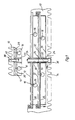
- Printed circuit boards 12 are held at their edges in a housing 10.
- the housing 10 consists of a good heat-conducting metal and is provided with cooling fins 14.
- the printed circuit boards 12 carry electrical components 16 on one side (bottom in FIG. 1).
- the components 16 extend in a conventional manner with connecting wires 18 through the printed circuit boards 12 and are on the other side (top side in FIG. 1) (solder side) soldered to conductor tracks.
- the printed circuit boards 12 carry a highly thermally conductive layer 20.
- the thermally conductive layer 20 is a heat-conducting sheet which is attached to the printed circuit board 12.
- the heat-conducting layer 20 is in additional heat-conducting contact with the housing 10 via a heat-conducting block 22, which is provided in a central region of the printed circuit board 12.
- the heat-conducting block 22 is a metal strip which is provided on the side of the heat-conducting layer 20 and is in heat-conducting contact therewith and extends across the printed circuit board 12.
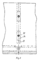
- the metal strip lugs 24 are provided which extend through the heat-conducting layer 20 and the printed circuit board 12. As can be seen from Fig. 2, in the preferred embodiment, the lugs 24 are elongated, extending along the metal bar.
- a plurality of circuit boards 12 are arranged parallel to one another and at a distance from one another.
- the heat-conducting block 22 of each printed circuit board 12 bears on the inner wall 26 of the housing 10 or on the lugs 24 of the heat-conducting block 22 of the adjacent printed circuit board 12, as shown in FIG. 1 for the upper of the two printed circuit boards 12 shown.
- the circuit boards 12 are arranged between and parallel to opposite inner walls 26 and 28 of the housing 10.
- the end plate on one side (the lowermost printed circuit board 12 in FIG. 1) lies with the heat-conducting block 22 on an inner wall 26 of the housing 10.
- the end plate on the other side (the uppermost printed circuit board 12 in FIG.
- the heat dissipation blocks 22 are preferably made of aluminum.
Description
Die Erfindung betrifft eine Vorrichtung zur Wärmeabfuhr von Leiterplatten, die an ihren Rändern in einem Gehäuse gehaltert sind und die auf einer Seite elektrische Bauteile tragen und auf der anderen Seite Leiterbahnen aufweisen, bei weicher
- (a) die Leiterplatten auf der besagten einen Seite eine gut wärmeleitende Schicht tragen, die an den Rändern der Leiterplatte mit gegenüberliegenden ersten Wandungsteilen des Gehäuses in wärmeleitender Verbindung steht.
- (a) the printed circuit boards on one side carry a good heat-conducting layer, which is in heat-conducting connection at the edges of the printed circuit board with opposite first wall parts of the housing.
Die auf Leiterplatten montierten elektrischen Bauteile können erhebliche Wärme erzeugen. Diese Wärme muss abgeführt werden, um die Gefahr einer Überhitzung und damit Beschädigung der Bauteile zu vermeiden. Ein weiteres Problem ergibt sich aus der häufig erhobenen Forderung, dass das Gerät beständig gegen Schwingungen ist und bestimmte Vibrationstests übersteht. Die nur an den Rändern eingespannten Leiterplatten neigen bei bestimmten Frequenzen zu Resonanzen. Diese können die Befestigung der Bauteile auf den Leiterplatten überproportional beanspruchen und zu Ausfällen führen.The electrical components mounted on printed circuit boards can generate considerable heat. This heat must be dissipated to avoid the risk of overheating and thus damage to the components. Another problem arises from the frequently raised requirement that the device is resistant to vibrations and that it passes certain vibration tests. The circuit boards clamped only at the edges tend to resonate at certain frequencies. These can disproportionately stress the mounting of the components on the printed circuit boards and lead to failures.
Durch die US-A-3 631 325 ist eine Leiterplattenanordnung mit einer Mehrzahl von parallel zueinander und im Abstand voneinander angeordneten Leiterplatten bekannt, die an ihren Rändern in einem Gehäuse gehaltert sind. Auf den Leiterplatten sind einzelne elektrische Bauteile angeordnet. Diese Bauteile sind in wärmeleitendem Kontakt mit Wärmeableitstreifen, die ebenfalls auf den Leiterplatten vorgesehen sind. Die Wärmeableitstreifen enden am Rand der Leiterplatte. Die Leiterplatte ist in Schlitze am Gehäuse einschiebbar, so dass die Wärme von den Wärmeableitstreifen auf das Gehäuse abgeleitet wird.US-A-3 631 325 discloses a printed circuit board arrangement with a plurality of printed circuit boards arranged parallel to one another and at a distance from one another, which are held at their edges in a housing. Individual electrical components are arranged on the printed circuit boards. These components are in heat-conducting contact with heat dissipation strips, which are also provided on the printed circuit boards. The heat dissipation strips end at the edge of the circuit board. The circuit board can be inserted into slots on the housing so that the heat is dissipated from the heat dissipation strips to the housing.
Bei dieser bekannten Anordnung erfolgt die Wärmeableitung ausschliesslich über die Ränder der Leiterplatten. Es ergibt sich weiterhin das schon oben erwähnte Problem der Resonanzschwingungen bei nur an den Rändern eingespannten Leiterplatten.In this known arrangement, the heat is dissipated exclusively via the edges of the circuit boards. The problem of resonance vibrations already mentioned above also arises with printed circuit boards clamped only at the edges.
Durch das DE-U-8 221 756.4 ist eine Einrichtung zur Wärmeableitung von thermisch belasteten Halbleiterchips bekannt. Die Halbleiterchips sind dabei zwischen zwei Klötzen eingespannt, so dass ihre elektrischen Anschlüsse auf den freien Seiten zwischen den Klötzen herausragen. Diese Anschlüsse sind abgebogen und mit einer Leiterplatte verlötet. Der obere Klotz besteht aus Aluminium und ist mit einer Platte verschraubt, die mit einem Kühlprofil in Verbindung steht. Der untere Klotz besteht aus Isolierstoff. Beide Klötze sind miteinander verschraubt.DE-U-8 221 756.4 discloses a device for heat dissipation from thermally loaded semiconductor chips. The semiconductor chips are clamped between two blocks, so that their electrical connections protrude on the free sides between the blocks. These connections are bent and soldered to a circuit board. The upper block is made of aluminum and is screwed to a plate that is connected to a cooling profile. The lower block is made of insulating material. Both blocks are screwed together.
Bei dieser bekannten Anordnung wird die Wärme von jedem Halbleiterchip einzeln mittels eines wärmeleitenden Klotzes auf eine Platte übertragen. Von der Platte fliesst die Wärme in der Ebene der Platte zu deren Rand, wo dieser mit dem Gehäuse verbunden ist. Die Platte entspricht daher der wärmeleitenden Schicht üblicher Leiterplatten. Es geht um das spezielle Problem der Übertragung der Wärme von Halbleiterchips auf diese wärmeleitende Schicht.In this known arrangement, the heat from each semiconductor chip is transferred individually to a plate by means of a heat-conducting block. The heat flows from the plate in the plane of the plate to its edge, where it is connected to the housing. The board therefore corresponds to the heat-conducting layer of conventional printed circuit boards. It is about the special problem of transferring the heat from semiconductor chips to this heat-conducting layer.
Die DE-A-1 243 252 betrifft eine Anordnung mit einer Mehrzahl zueinander paralleler, im Abstand voneinander in einem Gehäuse gehaltener Leiterplatten. Auf jeder der Leiterplatten liegt ein wärmeleitendes Blech als wärmeleitende Schicht auf. Leiterplatte und Blech sind mit gegenüberliegenden Rändern im Gehäuse gehaltert. Das Blech überträgt dabei Wärme auf das mit Kühlrippen versehene Gehäuse. Auch hier erfolgt also der Wärmetransport nur in der Ebene der Leiterplatten bis zu deren Rändern, über welche die Wärme auf das Gehäuse abgeleitet wird.DE-A-1 243 252 relates to an arrangement with a plurality of mutually parallel printed circuit boards which are spaced apart from one another in a housing. On each of the circuit boards there is a heat-conducting sheet as a heat-conducting layer. The printed circuit board and sheet metal are held in the housing with opposite edges. The sheet transfers heat to the housing with cooling fins. Here too, the heat is transported only in the plane of the printed circuit boards up to their edges, via which the heat is dissipated to the housing.
Die FR-A-2 413 016 beschreibt eine Kühlvorrichtung für einen Halbleiterchip, wobei die Schaltverbindungen durch eine mehrlagige Leiterplatte hergestellt sind. Der Halbleiterchip sitzt dabei unmittelbar auf einem zentralen Wärmeableitblock, der mit einer Metallplatte verbunden ist. Die mehrlagige Leiterplatte ist um den Wärmeableitblock herum angeordnet und liegt auf der Metallplatte auf. Es handelt sich hier ähnlich wie bei dem DE-U-8 221 756 um die Wärmeableitung von einem einzelnen Bauelement, nämlich dem Halbleiterchip, auf die Metallplatte, welche der üblichen wärmeleitenden Schicht entspricht. Es geht nicht um die Wärmeabfuhr von dieser Schicht zum Gehäuse.FR-A-2 413 016 describes a cooling device for a semiconductor chip, the switching connections being produced by a multilayer printed circuit board. The semiconductor chip sits directly on a central heat dissipation block, which is connected to a metal plate. The multilayer printed circuit board is arranged around the heat dissipation block and lies on the metal plate. Similar to DE-U-8 221 756, this is the heat dissipation from a single component, namely the semiconductor chip, onto the metal plate, which corresponds to the usual heat-conducting layer. It's not about dissipating heat from this layer to the case.
Die DE-A-2 744 341 betrifft eine Vorrichtung zur Aufnahme von Leiterplatten, bei welcher auch bei starken Beschleunigungen und Vibrationen eine Beschädigung der auf den Leiterplatten montierten Bauteile und ihrer Verbindungen vermieden wird. Dazu werden die Resonanzfrequenzen in solche Bereiche gelegt, in welchen die angreifenden Beschleunigungen einen geringen Pegel aufweisen. Dies wird dadurch erreicht, dass die Leiterplatten mit Seitenwänden verspannt sind, welche jede aus zwei miteinander vernieteten Blechen bestehen. Es erfolgt dann eine Reibungsdämpfung an den verschiedenen Berührungsflächen. Bauteile hoher Leistung, die starke Wärme erzeugen, sind gesondert auf einer Grundplatte montiert, von welcher die Wärme leichter abgeführt werden kann. Es geht hier nicht um das Problem der Wärmeleitung von Leiterplatten.DE-A-2 744 341 relates to a device for receiving printed circuit boards, in which damage to the components mounted on the printed circuit boards and their connections is avoided even under strong accelerations and vibrations. For this purpose, the resonance frequencies are placed in those areas in which the accelerations are at a low level. This is achieved in that the printed circuit boards are braced with side walls, which each consist of two riveted metal sheets. There is then frictional damping at the various contact surfaces. High-performance components that generate strong heat are mounted separately on a base plate from which the heat can be dissipated more easily. This is not about the problem of heat conduction on printed circuit boards.
Das DE-U-7 740 059 betrifft eine Befestigungsvorrichtung zur elektrisch isolierten Befestigung von Bauelementen, die eine erhebliche Verlustwärme erzeugen. Diese Bauelemente sind einzeln durch wärmeleitende Metallteile sowie durch Verbindungselemente aus Berylliumoxid mit dem Gehäuse verbunden. Dabei sind die Verbindungselemente durch Durchbrechungen einer Leiterplatte hindurchgeführt. Hier wird die Wärme von jedem einzelnen Bauelement über das Verbindungselement unmittelbar auf das Gehäuse abgeleitet. Es erfolgt also keine Wärmeableitung über eine wärmeleitende Schicht auf der Leiterplatte.DE-U-7 740 059 relates to a fastening device for the electrically insulated fastening of components which generate considerable heat loss. These components are individually connected to the housing by heat-conducting metal parts and by connecting elements made of beryllium oxide. The connecting elements are passed through openings in a printed circuit board. Here, the heat from each individual component is dissipated directly to the housing via the connecting element. So there is no heat dissipation via a heat-conducting layer on the circuit board.
Die DE-B-2 336 168 betrifft einen Horizontalablenk-Baustein, bei welchem eine Leiterplatte und eine Kühlfläche parallel zueinander liegend über Abstandshalter miteinander verbunden sind. Die Kühlfläche trägt ein Leistungs-Halbleiterbauelement, während die Leiterplatte weitere Bauelemente geringerer Verlustleistung trägt. Die Kühlfläche ist mit einem Metallrahmen des Fernsehempfängers verbunden.DE-B-2 336 168 relates to a horizontal deflection module in which a printed circuit board and a cooling surface are connected to one another in parallel to one another via spacers. The cooling surface carries a power semiconductor component, while the circuit board carries other components with lower power dissipation. The cooling surface is connected to a metal frame of the television receiver.
Der Erfindung liegt die Aufgabe zugrunde, bei einer Leiterplattenanordnung der eingangs genannten Art mit wenigstens einer, mit einer wärmeleitenden Schicht versehenen und an den Rändern im Gehäuse gehalterten Leiterplatte die Wärmeableitung von der Leiterplatte zu verbessern.The invention has for its object in a printed circuit board assembly of the type mentioned with at least one, provided with a heat-conducting layer and at the edges in Ge housing-mounted circuit board to improve heat dissipation from the circuit board.
Erfindungsgemäss wird diese Aufgabe mit einer Vorrichtung der eingangs genannten Art dadurch gelöst, dass
- (b) in einem Mittelbereich jeder Leiterplatte ein senkrecht zur Ebene der Leiterplatte vorstehender Wärmeableitblock vorgesehen ist, über den eine zusätzliche wärmeleitende Verbindung zwischen der Leiterplatte und einem zwischen den ersten Wandungsteilen sich im wesentlichen parallel zu der Leiterplatte erstreckenden zweiten Wandungsteil des Gehäuses hergestellt ist.
- (b) a heat dissipation block protruding perpendicular to the plane of the printed circuit board is provided in a central region of each printed circuit board, via which an additional heat-conducting connection between the printed circuit board and a second wall part of the housing extending essentially parallel to the printed circuit board is produced.
Es erfolgt auf diese Weise eine Ableitung von Wärme von den elektrischen Bauteilen über die wärmeleitende Schicht einmal zu den Rändern der Leiterplatte zu gegenüberliegenden ersten Wandungsteilen des Gehäuses und zum anderen vom Mittelbereich der Leiterplatte über die Wärmeleitblöcke zu wenigstens einem zweiten Wandungsteil des Gehäuses, der in der Regel senkrecht zu den ersten Wandungsteilen verläuft. Es wird dadurch die Wärmeableitung wesentlich verbessert, da der Weg der Wärme in der wärmeleitenden Schicht verringert wird. Ausserdem wird die Stabilität der Anordnung erhöht.In this way, heat is dissipated from the electrical components via the heat-conducting layer on the one hand to the edges of the circuit board to opposite first wall parts of the housing and on the other hand from the central region of the circuit board via the heat-conducting blocks to at least one second wall part of the housing, which is in the Usually runs perpendicular to the first wall parts. This significantly improves heat dissipation, since the path of heat in the heat-conducting layer is reduced. In addition, the stability of the arrangement is increased.
Ausgestaltungen der Erfindung sind Gegenstand der Unteransprüche.Embodiments of the invention are the subject of the dependent claims.
Ein Ausführungsbeispiel der Erfindung ist nachstehend unter Bezugnahme auf die zugehörigen Zeichnungen näher erläutert.
- Fig. 1 zeigt im Schnitt ein Gehäuse mit darin angeordneten Leiterplatten.
- Fig. 2 zeigt eine Draufsicht auf eine der Leiterplatten von der Lötseite her gesehen.
- Fig. 1 shows in section a housing with circuit boards arranged therein.
- Fig. 2 shows a plan view of one of the circuit boards seen from the solder side.
In einem Gehäuse 10 sind Leiterplatten 12 an ihren Rändern gehaltert. Das Gehäuse 10 besteht aus einem gut wärmeleitenden Metall und ist mit Kühlrippen 14 versehen. Die Leiterplatten 12 tragen auf einer Seite (unten in Fig. 1) elektrische Komponenten 16. Die Komponenten 16 erstrecken sich in üblicher Weise mit Anschlussdrähten 18 durch die Leiterplatten 12 hindurch und sind auf der anderen, in Fig. 1 oben liegenden Seite (Lötseite) mit Leiterbahnen verlötet.Printed
Auf der besagten Seite, aujf welcher die elektrischen Komponenten 16 sitzen, tragen die Leiterplatten 12 eine gut wärmeleitende Schicht 20. Bei der dargestellten bevorzugten Ausführung ist die wärmeleitende Schicht 20 ein Wärmeleitblech, das an der Leiterplatte 12 angebracht ist. Die wärmeleitende Schicht 20 steht über einen Wärmeleitblock 22, der in einem Mittelbereich der Leiterplatte 12 vorgesehen ist, mit dem Gehäuse 10 in zusätzlichem wärmeleitenden Kontakt. Bei der bevorzugten Ausführung ist der Wärmeleitblock 22 eine auf der Seite der wärmeleitenden Schicht 20 vorgesehene und mit dieser in wärmeleitendem Kontakt stehende Metallleiste, die sich quer über die Leiterplatte 12 erstreckt. An der Metalleiste sind Ansätze 24 vorgesehen, welche sich durch die wärmeleitende Schicht 20 und die Leiterplatte 12 erstrecken. Wie aus Fig. 2 ersichtlich ist, sind bei der bevorzugten Ausführungsform die Ansätze 24 langgestreckt, sich längs der Metalleiste erstreckend ausgebildet.On the said side, on which the
In dem Gehäuse 10 sind eine Mehrzahl von Leiterplatten 12 parallel zueinander und im Abstand voneinander angeordnet. Der Wärmeleitblock 22 jeder Leiterplatte 12 tiegt an der Innenwandung 26 des Gehäuses 10 bzw. an den Ansätzen 24 des Wärmeleitblocks 22 der benachbarten Leiterplatte 12 an, wie in Fig. 1 für die obere der beiden gezeichneten Leiterplatten 12 dargestellt ist. Die Leiterplatten 12 sind zwischen und parallel zu gegenüberliegenden Innenwandungen 26 und 28 des Gehäuses 10 angeordnet. Die Endplatte auf einer Seite (die unterste Leiterplatte 12 in Fig. 1) liegt mit dem Wärmeleitblock 22 an einer Innenwand 26 des Gehäuses 10 an. Die Endplatte auf der anderen Seite (die oberste Leiterplatte 12 in Fig. 1) liegt mit den besagten Ansätzen 24 des Wärmeleitblocks 22 an der gegenüberliegenden Innenwandung 28 an. In den Wärmeleitblöcken 22 und den Ansätzen 24 der parallel übereinander angeordneten Leiterplatten 12 sind fluchtende Bohrungen 30 vorgesehen. Durch die Bohrungen sind Schraubbolzen 32 geführt. Die Schraubbolzen 32 sind durch Bohrungen 34 des Gehäuses 10 auf einer Seite hindurchgeführt und liegen mit ihren Köpfen 36 dort auf der Aussenseite des Gehäuses 10 auf. Mit Gewinden 38 sind die Schraubbolzen 32 in Gewindebohrungen 40 auf der gegenüberliegenden Seite des Gehäuses eingeschraubt. Es können dann durch Festziehen der Schraubbolzen die gegenüberliegenden Wandungen des Gehäuses 10 und die dazwischenliegenden Wärmeableitblöcke 22 gegeneinandergezogen werden, was den thermischen Kontakt verbessert. Die Wärmeableitblöcke 22 sind vorzugsweise aus Aluminium hergestellt.In the
Claims (6)
characterized in that
Applications Claiming Priority (2)
| Application Number | Priority Date | Filing Date | Title |
|---|---|---|---|
| DE3331112 | 1983-08-30 | ||
| DE19833331112 DE3331112A1 (en) | 1983-08-30 | 1983-08-30 | DEVICE FOR HEAT EXHAUST FROM PCB |
Publications (2)
| Publication Number | Publication Date |
|---|---|
| EP0136454A1 EP0136454A1 (en) | 1985-04-10 |
| EP0136454B1 true EP0136454B1 (en) | 1987-05-13 |
Family
ID=6207712
Family Applications (1)
| Application Number | Title | Priority Date | Filing Date |
|---|---|---|---|
| EP84108975A Expired EP0136454B1 (en) | 1983-08-30 | 1984-07-28 | Device for the heat dissipation of printed circuit boards |
Country Status (3)
| Country | Link |
|---|---|
| US (1) | US4583149A (en) |
| EP (1) | EP0136454B1 (en) |
| DE (2) | DE3331112A1 (en) |
Families Citing this family (12)
| Publication number | Priority date | Publication date | Assignee | Title |
|---|---|---|---|---|
| DE3536963A1 (en) * | 1985-10-17 | 1987-04-23 | Diehl Gmbh & Co | ASSEMBLY ARRANGEMENT |
| DE3813364A1 (en) * | 1988-04-21 | 1989-11-02 | Bodenseewerk Geraetetech | DEVICE FOR HEAT EXHAUSTING COMPONENTS ON A CIRCUIT BOARD |
| US5329420A (en) * | 1990-02-28 | 1994-07-12 | Altoz Frank E | Slotted tuning fork thermal interface |
| GB2259408A (en) * | 1991-09-07 | 1993-03-10 | Motorola Israel Ltd | A heat dissipation device |
| DE4310446C1 (en) * | 1993-03-31 | 1994-05-05 | Export Contor Ausenhandelsgese | Power semiconductor circuit module - has mirror symmetrical configuration of power semiconductor carrier plates and heat sink elements |
| WO1996013048A1 (en) * | 1994-10-19 | 1996-05-02 | Philips Electronics N.V. | Electric lamp |
| US5506751A (en) * | 1994-10-26 | 1996-04-09 | Chatel; Louis R. | Extruded card cage |
| US6086404A (en) * | 1998-07-02 | 2000-07-11 | Advanced Processing Laboratories, Inc. | Circuit board card cage with one-piece integral card guide units |
| US5986887A (en) * | 1998-10-28 | 1999-11-16 | Unisys Corporation | Stacked circuit board assembly adapted for heat dissipation |
| FR2821497B1 (en) * | 2001-02-27 | 2004-07-16 | Bosch Gmbh Robert | ELECTRIC DRIVE, PARTICULARLY WINDSCREEN WIPER DRIVE |
| US7046520B2 (en) * | 2003-04-07 | 2006-05-16 | Honeywell International, Inc. | Electronic assemblies having supports for circuit boards |
| DE102008033193A1 (en) | 2008-07-15 | 2010-02-04 | Continental Automotive Gmbh | Motor control device of a vehicle |
Citations (4)
| Publication number | Priority date | Publication date | Assignee | Title |
|---|---|---|---|---|
| DE1243252B (en) * | 1965-05-17 | 1967-06-29 | Int Standard Electric Corp | Housing for receiving printed circuit boards, which is made of sheet metal parts closed on all sides |
| US3631325A (en) * | 1970-06-15 | 1971-12-28 | Sperry Rand Corp | Card module and end wall treatment facilitating heat transfer and sliding |
| DE2744341A1 (en) * | 1977-10-01 | 1979-04-12 | Teldix Gmbh | Frame holding circuit boards - has sides clamping spaced boards and having two riveted plates to prevent vibration or acceleration damage |
| DE8221756U1 (en) * | 1982-07-30 | 1982-11-04 | Siemens AG, 1000 Berlin und 8000 München | Device for heat dissipation from thermally stressed flat components in communications technology |
Family Cites Families (6)
| Publication number | Priority date | Publication date | Assignee | Title |
|---|---|---|---|---|
| US3487267A (en) * | 1968-01-02 | 1969-12-30 | Jerrold Electronics Corp | Thermally conducting transistor support arms |
| DE2336168B1 (en) * | 1973-07-16 | 1974-10-03 | Siemens Ag | Horizontal deflection block |
| FR2413016A1 (en) * | 1977-12-26 | 1979-07-20 | Radiotechnique Compelec | Multilayer printed circuits with heat dissipation collector - has thermal drain attached to semiconductor substrate pressed into hole in collector plate |
| DE7740059U1 (en) * | 1977-12-29 | 1980-04-03 | Neumann Elektronik Gmbh, 4330 Muelheim | Fastening device for the electrically insulated fastening of components that generate considerable heat loss |
| US4386390A (en) * | 1981-01-21 | 1983-05-31 | The Bendix Corporation | Vibration adjustable spacer |
| US4475145A (en) * | 1982-07-12 | 1984-10-02 | Rockwell International Corporation | Circuit board heatsink assembly and technique |
-
1983
- 1983-08-30 DE DE19833331112 patent/DE3331112A1/en not_active Withdrawn
-
1984
- 1984-07-28 EP EP84108975A patent/EP0136454B1/en not_active Expired
- 1984-07-28 DE DE8484108975T patent/DE3463719D1/en not_active Expired
- 1984-08-13 US US06/639,833 patent/US4583149A/en not_active Expired - Fee Related
Patent Citations (4)
| Publication number | Priority date | Publication date | Assignee | Title |
|---|---|---|---|---|
| DE1243252B (en) * | 1965-05-17 | 1967-06-29 | Int Standard Electric Corp | Housing for receiving printed circuit boards, which is made of sheet metal parts closed on all sides |
| US3631325A (en) * | 1970-06-15 | 1971-12-28 | Sperry Rand Corp | Card module and end wall treatment facilitating heat transfer and sliding |
| DE2744341A1 (en) * | 1977-10-01 | 1979-04-12 | Teldix Gmbh | Frame holding circuit boards - has sides clamping spaced boards and having two riveted plates to prevent vibration or acceleration damage |
| DE8221756U1 (en) * | 1982-07-30 | 1982-11-04 | Siemens AG, 1000 Berlin und 8000 München | Device for heat dissipation from thermally stressed flat components in communications technology |
Also Published As
| Publication number | Publication date |
|---|---|
| US4583149A (en) | 1986-04-15 |
| EP0136454A1 (en) | 1985-04-10 |
| DE3463719D1 (en) | 1987-06-19 |
| DE3331112A1 (en) | 1985-03-14 |
Similar Documents
| Publication | Publication Date | Title |
|---|---|---|
| EP0920055B1 (en) | Cooling device for a heat generating component on a printed board | |
| EP0590354B1 (en) | Device with a board, a heat sink and at least one power component | |
| DE112008000452B4 (en) | Semiconductor module and inverter device | |
| DE69637488T2 (en) | Semiconductor and semiconductor module | |
| WO1994029901A1 (en) | Securing device for semiconductor circuit components | |
| EP0136454B1 (en) | Device for the heat dissipation of printed circuit boards | |
| DE19634202C2 (en) | Semiconductor device | |
| DE102006045939A1 (en) | Power semiconductor module with improved thermal shock resistance | |
| DE4335946C2 (en) | Arrangement consisting of a printed circuit board | |
| DE4027072A1 (en) | SEMICONDUCTOR ARRANGEMENT | |
| DE102021132148A1 (en) | circuit board arrangement | |
| DE3940521A1 (en) | COLD AREA SYSTEM FOR COOLING ELECTRONIC COMPONENTS | |
| EP1445799A2 (en) | Heat dissipation device for a semiconductor on a printed circuit board | |
| DE102008003787B4 (en) | PCB layout | |
| DE4226816C2 (en) | Device for heat dissipation from a housing of an integrated circuit | |
| DE202019105232U1 (en) | Spliced multilayer printed circuit board | |
| DE3237878C2 (en) | Arrangement for dissipating the heat loss of a semiconductor component mounted on a printed circuit board | |
| DE3614086C2 (en) | Device for heat dissipation from a unit containing electronic components and method for thermally coupling a unit containing electronic components | |
| EP0652694B1 (en) | Control apparatus for vehicle | |
| DE102005026233B4 (en) | Electric power module | |
| EP0180730B1 (en) | Arrangement for the tension compensation and the heat dissipation of an electronic component | |
| EP0113794A1 (en) | Support for component parts | |
| EP1393375B1 (en) | Contact system | |
| DE3628556C1 (en) | Semiconductor device | |
| DE19805492C2 (en) | Circuit board |
Legal Events
| Date | Code | Title | Description |
|---|---|---|---|
| PUAI | Public reference made under article 153(3) epc to a published international application that has entered the european phase |
Free format text: ORIGINAL CODE: 0009012 |
|
| AK | Designated contracting states |
Designated state(s): DE FR GB |
|
| 17P | Request for examination filed |
Effective date: 19850306 |
|
| RTI1 | Title (correction) | ||
| 17Q | First examination report despatched |
Effective date: 19860923 |
|
| GRAA | (expected) grant |
Free format text: ORIGINAL CODE: 0009210 |
|
| AK | Designated contracting states |
Kind code of ref document: B1 Designated state(s): DE FR GB |
|
| REF | Corresponds to: |
Ref document number: 3463719 Country of ref document: DE Date of ref document: 19870619 |
|
| ET | Fr: translation filed | ||
| PLBE | No opposition filed within time limit |
Free format text: ORIGINAL CODE: 0009261 |
|
| STAA | Information on the status of an ep patent application or granted ep patent |
Free format text: STATUS: NO OPPOSITION FILED WITHIN TIME LIMIT |
|
| 26N | No opposition filed | ||
| PGFP | Annual fee paid to national office [announced via postgrant information from national office to epo] |
Ref country code: FR Payment date: 19980604 Year of fee payment: 15 |
|
| PGFP | Annual fee paid to national office [announced via postgrant information from national office to epo] |
Ref country code: GB Payment date: 19980716 Year of fee payment: 15 |
|
| PGFP | Annual fee paid to national office [announced via postgrant information from national office to epo] |
Ref country code: DE Payment date: 19980922 Year of fee payment: 15 |
|
| PG25 | Lapsed in a contracting state [announced via postgrant information from national office to epo] |
Ref country code: GB Free format text: LAPSE BECAUSE OF NON-PAYMENT OF DUE FEES Effective date: 19990728 |
|
| PG25 | Lapsed in a contracting state [announced via postgrant information from national office to epo] |
Ref country code: FR Free format text: THE PATENT HAS BEEN ANNULLED BY A DECISION OF A NATIONAL AUTHORITY Effective date: 19990731 |
|
| GBPC | Gb: european patent ceased through non-payment of renewal fee |
Effective date: 19990728 |
|
| PG25 | Lapsed in a contracting state [announced via postgrant information from national office to epo] |
Ref country code: DE Free format text: LAPSE BECAUSE OF NON-PAYMENT OF DUE FEES Effective date: 20000503 |
|
| REG | Reference to a national code |
Ref country code: FR Ref legal event code: ST |