EP0135136A2 - Integrated RS flipflop circuit - Google Patents
Integrated RS flipflop circuit Download PDFInfo
- Publication number
- EP0135136A2 EP0135136A2 EP84109633A EP84109633A EP0135136A2 EP 0135136 A2 EP0135136 A2 EP 0135136A2 EP 84109633 A EP84109633 A EP 84109633A EP 84109633 A EP84109633 A EP 84109633A EP 0135136 A2 EP0135136 A2 EP 0135136A2
- Authority
- EP
- European Patent Office
- Prior art keywords
- layer
- flip
- integrated
- flop circuit
- circuit according
- Prior art date
- Legal status (The legal status is an assumption and is not a legal conclusion. Google has not performed a legal analysis and makes no representation as to the accuracy of the status listed.)
- Ceased
Links
Images

Classifications
-
- H—ELECTRICITY
- H03—ELECTRONIC CIRCUITRY
- H03K—PULSE TECHNIQUE
- H03K3/00—Circuits for generating electric pulses; Monostable, bistable or multistable circuits
- H03K3/02—Generators characterised by the type of circuit or by the means used for producing pulses
- H03K3/353—Generators characterised by the type of circuit or by the means used for producing pulses by the use, as active elements, of field-effect transistors with internal or external positive feedback
- H03K3/356—Bistable circuits
- H03K3/356017—Bistable circuits using additional transistors in the input circuit
Definitions
- the invention relates to an integrated RS flip-flop circuit according to the preamble of claim 1 and to its use as a semiconductor memory cell.
- a flip-flop circuit of this type is known from the book "Microelectronic Circuits" by A. Möschwitzer and G. Jorke, VEB Verlagtechnik, Berlin, 1979, p. 118, Fig. 2.37c.
- the switching elements are also implemented as field effect transistors, which are connected in parallel to the field effect transistors of the cross-coupled inverters with their source-drain paths and with their gate connections represent the R or S input.
- the invention is based on the object of specifying an integrated RS flip-flop circuit which can be implemented on a substantially smaller semiconductor area than comparable conventional circuits. According to the invention this is achieved by training according to the characterizing part of patent claim 1.
- the advantage that can be achieved with the invention is, in particular, that the field effect transistor taking over the switching function of each inverter, together with the switching element assigned to it, consists of a single semiconductor component which takes over two transistor functions and only requires the semiconductor area of a single MIS field effect transistor for implementation.
- the switching speed at the R and S inputs is also greatly increased compared to conventional circuits.
- Claims 2 to 10 are directed to preferred refinements and developments of the invention, while claim 11 relates to the use of the RS flip-flop circuit as a memory cell.
- the first inverter consists of the series connection of a field effect transistor T1 and a resistance element R1, the end connections 1 and 2 of the series connection each being connected to the supply voltage V DD and the reference potential.
- the second inverter which comprises a field effect transistor T2 and a resistance element R2, is also connected to the terminals 1, 2. Between T1 and R1 there is a circuit node 3, which is connected to the gate of T2, between T2 and R2 a circuit node 4, which is led to the gate of T1.
- the resistance elements R1 and R2 which are shown in FIG.
- depletion-type field effect transistors the gate electrodes of which are connected to the source connections
- the circuit nodes 4 and 3 simultaneously represent the output Q and the inverse output Q of the flip-flop circuit.
- T3 denotes a hot electron transistor of the tunnel emission type, which is combined with transistor T1 to form a component 5.
- Another hot electron transistor T4 is combined with the field effect transistor T2 to form a component 6.
- the base connections of the transistors T3 and T4 are provided with connecting lines 7 and 8 which are connected to the R or. S input of the circuit are connected.
- the collector connection 9 of T3 is connected to the circuit node 4, the collector connection 10 of T4 to the circuit node 3.
- Hot electron transistors are e.g. from Solid-State Electronics, Vol. 24, 1981, pp. 343-366, in particular Fig. 1.
- FIG. 2 shows the semiconductor component denoted by 5 in FIG. 1 in cross section. It is arranged on a body 11 made of doped semiconductor material, for example p-doped silicon with an impurity concentration of approximately 10 15 / cm 3 , into which two, for example n T- doped regions 12 and 13 starting from an interface 11a are inserted. These represent the source region and the drain region of the field effect transistor T1, the gate electrode of which consists of two parts.
- the first part is formed by a metallic or metallically conductive layer 15, which covers the part 14a of the channel region -14 lying between the region 12 and the region 12.
- a very thin insulator layer 16 lies between the layer 15 and the interface 11a.
- the thickness of the insulator layer 16 consisting, for example, of Si0 2 or Si 3 N 4 is expediently about 2 to 5 nm.
- the layer 15 advantageously consists of a high-melting metal, for example of Ta, Ti or Mo or W, or of the silicide of one of these Metals, ie made of TaSi 2 , TiSi 2 , MoSi 2 or WSi 2 , and can have a thickness of approximately 10 nm.
- a polycrystalline silicon layer 17 with a thickness of approximately 10 to 100 nm and preferably with a p-doping, which is approximately given by a doping concentration of 10 14 to 10 15 / cm 3 , boron being used as the dopant can be.
- the layer 17 there is a metallic or metallically conductive layer 18, the thickness of which can be chosen as desired, but is expediently greater than the layer thickness of 17.
- the layer 18 advantageously consists of one of the metals or silicides which are already in connection have been mentioned with the layer 15.
- the layers 17 and 18 cover the entire channel region 14, the part of 18 which laterally projects beyond the layer 15 forming the second part of the gate electrode and as such covering part 14b of the channel region 14.
- An electrically insulating layer (field oxide layer) covering the surface 11a outside the parts 12 to 14 has parts 19 laterally adjacent to the layers 17 and 18.
- the source region 12 is connected to the connection 2, the drain region 13 to the circuit node 3.
- the semiconductor body 11 is connected to the reference potential at 20. Furthermore, the base layer 15 is connected to the input R, while the layer 18 is provided with the collector connection 9.
- the inversion layer 21a represents the emitter layer of a tunnel emission type hot electron transistor (HET), which additionally has the layers 15, 16, 17 and 18.
- HET tunnel emission type hot electron transistor
- the layer 15 forms a metallic or metallic conductive base layer of the HET, the insulator layer 16 being located between the layer 15 and the emitter layer 21a, while the polycrystalline silicon layer 17 together with the metallic or metallic conductive layer 18 represents the collector layer of the HET .
- the layer 18 is supplied with a collector voltage, which in FIG. 1 consists of the voltage at the circuit node 4. If this voltage exceeds a second threshold voltage, which is assigned to the part 14b of the channel region 14, an inversion layer 21b is formed below the part of the layer 18 laterally projecting the layer 15, which together with the inversion layer 21a forms an n-conducting channel between the Areas 12 and 13 forms.
- a part 16a of the insulator layer 16 which, for example, is 15 nm much thicker than the other parts of this layer, is located between the second part of the gate electrode formed by the layer 18 and the part 14b of the channel region 14, is partly responsible for the fact that the second threshold voltage is higher than the first.
- the said depletion zone and the inversion layer 21a below 15 are also built up when there is a voltage above the second threshold voltage at terminal 9 when terminal R is dead.
- the function of the HET will be explained below using the energetic band structure diagram shown in FIG. This shows energy states E plotted in the direction of the vertical axis, which occur as a function of different distances x from the inversion layer or emitter layer 21a.
- the layers 21a, 16, 15, 17 and 18 are assigned successive sections of the x-axis, the lengths d21a, d16, d15, d17 and d18 of these sections being dependent on the actual layer thicknesses D21a, D16, D15, D17 for reasons of clear illustration and D18 of layers 21a, 16, 15, 17 and 18 differ.
- section d16 is greatly stretched compared to sections d15, d17, d18 and d21a.
- the upper limit of the valence band of the semiconductor material of FIG. 11 is designated E v1
- E c1 represents the energy level of the electrons within inversion layer 21a.
- the upper line E c16 the lower limit of the conduction band of the insulator layer 16
- the lower line E v16 means the upper limit of the valence band.
- the respective Fermi levels E F15 and E F18 are entered in sections d15 and d18, while in section d17 the lower limit of the conduction band of layer 17 is represented by E c17 and the upper limit of the valence band by E v17 .
- the semiconductor component 6 is constructed analogously to 5 and is provided with the connections 2, 4, 10 and S in accordance with FIG. 1.
- a voltage corresponding to the supply voltage V DD which corresponds to a logic "1" can be tapped at the output Q, while the output Q approximately Reference potential lies, which corresponds to a logical "0".
- the voltage which can be tapped at the output Q or at the circuit node 4 is also at the collector connection 9 of 5. This voltage is so great that both the first threshold voltage of 14a and the second threshold voltage of 14b are exceeded in the transistor T1, and the inversion layers. 21a and 21b form a conductive channel between regions 12 and 13.
- the voltage occurring at the circuit node 3 in this switching state is so small that the two threshold voltages of the transistor T2 are undershot, so that T2 blocks.
- a voltage pulse is now fed to the input R, which positively prestresses the base layer 15 with respect to the inversion layer 21a of the transistor T1, electrons from 21a of the tunnel effect through the insulator layer 16 into the base layer 15 and further to the collector layer 18.
- a current flows in the circuit branch 1, R2, 4, 9, T3 and 2, which causes a voltage drop at R2.
- the voltage at 4 or at connection 9 of 5 is reduced by this voltage drop.
- the voltage drops below the second threshold voltage of T1, so that T1 blocks.
- the voltage at the circuit node 3 rises almost to the value of the supply voltage V DD , so that a gate voltage of such a magnitude is supplied via the terminal 10 that the inversion layers 21a and 21b of T2 are built up and T2 comes into the current-carrying state .
- the flip-flop circuit is in the reset state.
- the emitter-base circuit of the HET T3 is de-energized after the voltage pulse at R has been switched off and the resulting drop below the first threshold voltage.
- the manufacture of the semiconductor component according to FIG. 2 initially corresponds to the usual manufacture of a field effect transistor. After a field oxide layer 19 covering the entire surface of the semiconductor body 11 An etching mask is applied to the insulator layer above the channel region 14 and the regions 12 and 13 and an insulator layer having a thickness of, for example, 15 nm, which corresponds approximately to the thickness of the part 16a in FIG with its opening only leaves the area of the metallically conductive layer 15 free. In this area, the insulator layer is etched to a thickness of approximately 2 to 5 nm, for example by an etchant based on fluorine-hydrogen, which is indicated in FIG. 2 by the reduced thickness of layer 16 above 14a. The layer 15 is then applied using the same intermediate mask.
- a further mask is applied which contains an opening which defines the lateral dimensions of the layers 17 and 18.
- the layers 17 and 18 are then applied in succession.
- the layer 17 is provided with a p-type impurity whose concentration is from 1 0 14 to 10 15 / cm 3 before the layer is applied 18th
- a dopant is implanted to produce regions 12 and 13, layers 15, 17 and 18 and the field oxide layer serving as parts of a doping mask (self-adjustment).
- connection line is laid, which leads to connection 9.
- the semiconductor component 5 or 6 is on one Body 11 made of a p-doped III-V semiconductor compound, for example GaAs with a doping concentration of z . B. 10 16 / cm 3 , built up, the insulator layer 16 advantageously consists of AlGaAs.
- the polycrystalline silicon layer 17 is replaced by a layer of p-doped GaAs with Be as the dopant, while the layer 15 is preferably formed from a highly doped n-type III-V semiconductor compound, for example GaAs with Si as the dopant behaves similar to a metal in terms of its electrical conductivity with a doping concentration of around 1018 / cm3.
- Layer 18 also advantageously consists of the same material as layer 15.
- the semiconductor component 5 or 6 is designed such that a second insulator layer takes the place of the previously described layer 17, the structure and thickness of which preferably corresponds to the insulator layer 16.
- the second insulator layer consists of Si0 2 or Si 3 N 4 , in the case of a semiconductor body made of GaAs, AlGaAs. Their thickness is advantageously about 2 to 5 nm.
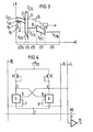
- connection 4 shows the use of the flip-flop circuit according to the invention as a static memory cell.
- the circuit shown in FIG. 1 is supplemented to the extent that the connection 2 is connected to a word line WL which is used for addressing the memory cell, while the connection lines 8 and 7 are each connected to a bit line BL and a second bit line BL , which leads an inverse signal to the -BL.
- the circuit node 4 (or the circuit node 3) is finally connected to a read line LL.
- a large number of such memory cells are usually arranged in several rows and columns arranged one above the other, with the memory cells lying in one row lying on the same word line WL, while all the memory cells located in a column are connected to the same bit lines and the same read line.
- the read line LL is routed to the input of a sense amplifier LV, at the output 26 of which the memory signal read out can be tapped.
- the word line WL is at a potential V which corresponds to a logic "1” on the line BL or BL or exceeds it or is less than such a "1” by less than the value of the first threshold voltage of T1 or T2.
- V a potential which corresponds to a logic "1” on the line BL or BL or exceeds it or is less than such a "1” by less than the value of the first threshold voltage of T1 or T2.
- the respective stored signal is then read after the potential has been lowered from WL to approximately reference potential via the line LL, the input of the sense amplifier LV having a "1" being read out Signal is occupied, but not when reading a "0".
- the "1" signals on the bit lines BL and BL must be greater by the amount of the base emitter voltage V R (FIG. 3) than the potential to which the word line WL is lowered when the cell is selected.
Abstract
Integrierte RS-Flipflop-Schaltung mit zwei kreuzgekoppelten Invertern, die jeweils aus einem Feldeffekttransistor (T1, T2) und einem in Serie geschalteten Widerstandselement (R1, R2) bestehen. Jeder Feldeffekttransistor ist mit einem zusätzlichen Schaltelement (T3, T4) verbunden, dessen Steuereingang den R- bzw. S-Eingang darstellt. Angestrebt wird eine Realisierung der Flipflopschaltung auf einer möglichst kleinen Halbleiterfläche. Das wird erreicht durch eine Ausbildung der zusätzlichen Schaltelemente (T3, T4) als Heiße-Elektronen-Transistoren, von denen jeder mit einem der Feldeffekttransistoren (T1, T2) zu einem gemeinsamen Bauelement (5, 6) zusammengefaßt wird, das zwei Transistorfunktionen übernimmt, aber nur die Fläche eines Feldeffekttransistors benötigt. Der Anwendungsbereich umfaßt hochintegrierte Schaltungskreise.Integrated RS flip-flop circuit with two cross-coupled inverters, each consisting of a field effect transistor (T1, T2) and a series-connected resistance element (R1, R2). Each field effect transistor is connected to an additional switching element (T3, T4), the control input of which represents the R or S input. The aim is to implement the flip-flop circuit on the smallest possible semiconductor area. This is achieved by designing the additional switching elements (T3, T4) as hot electron transistors, each of which is combined with one of the field effect transistors (T1, T2) to form a common component (5, 6) that takes over two transistor functions, but only needs the area of a field effect transistor. The field of application includes highly integrated circuits.
Description
Die Erfindung bezieht sich auf eine integrierte RS-Flipflop-Schaltung nach dem Oberbegriff des Patentanspruchs 1 und auf deren Verwendung als Halbleiterspeicherzelle.The invention relates to an integrated RS flip-flop circuit according to the preamble of claim 1 and to its use as a semiconductor memory cell.
Eine Flipflop-Schaltung dieser Art ist aus dem Buch "Mikroelektronische Schaltkreise" von A. Möschwitzer und G. Jorke, VEB Verlag Technik, Berlin, 1979, S. 118, Bild 2.37c, bekannt. Dabei sind die Schaltelemente ebenfalls als Feldeffekttransistoren realisiert, die den Feldeffekttransistoren der kreuzgekoppelten Inverter mit ihren Source-Drain-Strecken parallel geschaltet sind und mit ihren Gateanschlüssen den R- bzw. S-Eingang darstellen.A flip-flop circuit of this type is known from the book "Microelectronic Circuits" by A. Möschwitzer and G. Jorke, VEB Verlag Technik, Berlin, 1979, p. 118, Fig. 2.37c. The switching elements are also implemented as field effect transistors, which are connected in parallel to the field effect transistors of the cross-coupled inverters with their source-drain paths and with their gate connections represent the R or S input.
Der Erfindung liegt die Aufgabe zugrunde, eine integrierte RS-Flipflop-Schaltung anzugeben, die auf einer wesentlich kleineren Halbleiterfläche realisiert werden kann, als vergleichbare herkömmliche Schaltungen. Erfindungsgemäß wird dies durch eine Ausbildung nach dem kennzeichnenden Teil des Patentanspruchs 1 erreicht.The invention is based on the object of specifying an integrated RS flip-flop circuit which can be implemented on a substantially smaller semiconductor area than comparable conventional circuits. According to the invention this is achieved by training according to the characterizing part of patent claim 1.
Der mit der Erfindung erzielbare Vorteil besteht insbesondere darin, daß der die Schaltfunktion übernehmende Feldeffekttransistor jedes Inverters zusammen mit dem ihm zugeordneten Schaltelement aus einem einzigen Halbleiterbauelement besteht, das zwei Transistorfunktionen übernimmt und zur Realisierung lediglich die Halbleiterfläche eines einzigen MIS-Feldeffekttransistors benötigt. Die Schaltgeschwindigkeit am R- und S-Eingang ist außerdem gegenüber herkömmmlichen Schaltungen stark erhöht. Die Ansprüche 2 bis 10 sind auf bevorzugte Ausgestaltungen und Weiterbildungen der Erfindung gerichtet, während der Anspruch 11 die Verwendung der RS-Flipflop- Schaltung als Speicherzelle betrifft.The advantage that can be achieved with the invention is, in particular, that the field effect transistor taking over the switching function of each inverter, together with the switching element assigned to it, consists of a single semiconductor component which takes over two transistor functions and only requires the semiconductor area of a single MIS field effect transistor for implementation. The switching speed at the R and S inputs is also greatly increased compared to conventional circuits.
Nachfolgend wird die Erfindung anhand der Zeichnungen näher erläutert. Dabei zeigt:
- Fig. 1 ein erfindungsgemäß ausgebildetes RS-Flipflop,
- Fig. 2 den Querschnitt eines in Fig. 1 schematisch dargestellten Bauelements, das einen MIS-Feldeffekttransistor und einen Heiße-Elektronen-TransisTor aufweist,
- Fig. 3 ein Bandstrukturschema zur Erläuterung von Fig. 2 und
- Fig. 4 ein erfindungsgemäßes RS-Flipflop, das als eine statische Speicherzelle verwendet wird.
- 1 shows an RS flip-flop designed according to the invention,
- 2 shows the cross section of a component shown schematically in FIG. 1, which has an MIS field-effect transistor and a hot electron transistor,
- Fig. 3 is a band structure diagram for explaining Fig. 2 and
- Fig. 4 shows an RS flip-flop according to the invention, which is used as a static memory cell.
In Fig. 1 sind zwei kreuzgekoppelte Inverter dargestellt, die eine Flipflop-Schaltung bilden. Der erste Inverter besteht aus der Serienschaltung eines Feldeffekttransistors T1 und eines Widerstandselementes R1, wobei die endseitigen Anschlüsse 1 und 2 der Serienschaltung jeweils mit der Versorgungsspannung VDD und dem Bezugspotential beschaltet sind. Der zweite Inverter, der einen Feldeffekttransistor T2 und ein Widerstandselement R2 umfaßt, liegt ebenfalls an den Anschlüssen 1, 2. Zwischen T1 und R1 befindet sich ein Schaltungsknoten 3, der mit dem Gate von T2 verbunden ist, zwischen T2 und R2 ein Schaltungsknoten 4, der an das Gate von T1 geführt ist. Die Widerstandselemente R1 und R2, die in Fig. 1 als Feldeffekttransistoren des Verarmungstyps dargestellt sind, deren Gateelektroden mit den Sourceanschlüssen verbunden sind, können auch in anderer Weise realisiert werden, so z.B. als Feldeffekttransistoren des Anreicherungstyps, deren Gateelektroden mit den Drainanschlüssen verbunden sind, als streifenförmige Strukturen aus widerstandsbehafterem Material oder dgl.. Die Schaltungsknoten 4 und 3 stellen gleichzeitig den Ausgang Q und den inversen Ausgang Q der Flipflop-Schaltung dar.1 shows two cross-coupled inverters which form a flip-flop circuit. The first inverter consists of the series connection of a field effect transistor T1 and a resistance element R1, the
Mit T3 ist ein Heiße-Elektronen-Transistor des Tunnelemissionstyps bezeichnet, der mit dem Transistor T1 zu einem Bauelement 5 zusammengefaßt ist. Ein weiterer Heiße-Elektronen-Transistor T4 ist mit dem Feldeffekttransistor T2 zu einem Bauelement 6 zusammengefaßt. Dabei sind die Basisanschlüsse der Transistoren T3 und T4 mit Anschlußleitungen 7 und 8 versehen, die mit dem R-bzw. S-Eingang der Schaltung verbunden sind. Der Kollektoranschluß 9 von T3 ist mit dem Schaltungsknoten 4 beschaltet, der Kollektoranschluß 10 von T4 mit dem Schaltungsknoten 3. Heiße-Elektronen-Transistoren sind z.B. aus Solid-State Electronics, Bd. 24, 1981, S. 343 - 366, insbesondere Fig. 1, bekannt.T3 denotes a hot electron transistor of the tunnel emission type, which is combined with transistor T1 to form a
Fig. 2 zeigt das in Fig. 1 mit 5 bezeichnete Halbleiter- Bauelement im Querschnitt. Es ist auf einem Körper 11 aus dotiertem Halbleitermaterial, z.B. p-dotiertem Silizium mit einer Störstellenkonzentration von etwa 1015/cm3, angeordnet, in den zwei von einer Grenzfläche 11a ausgehende, z.B. nT-dotierte Gebiete 12 und 13 eingefügt sind. Diese stellen das Sourcegebiet und das Draingebiet des Feldeffekttransistors T1 dar, dessen Gateelektrode aus zwei Teilen besteht. Der erste Teil wird von einer metallischen bzw. metallisch leitenden Schicht 15 gebildet, die den an das Gebiet 12 grenzenden Teil 14a des zwischen 12 und 13 liegenden Kanalbereichs -14 überdeckt. Zwischen der Schicht 15 und der-Grenzfläche 11a liegt dabei eine sehr dünne Isolatorschicht 16.FIG. 2 shows the semiconductor component denoted by 5 in FIG. 1 in cross section. It is arranged on a body 11 made of doped semiconductor material, for example p-doped silicon with an impurity concentration of approximately 10 15 / cm 3 , into which two, for example n T- doped
Die Dicke der z.B. aus Si02 oder Si3N4 bestehenden Isolatorschicht 16 beträgt zweckmäßigerweise etwa 2 bis 5 nm. Die Schicht 15 besteht mit Vorteil aus einem hochschmelzenden Metall, z.B. aus Ta, Ti oder Mo oder W, oder aus dem Silizid eines dieser Metalle, d.h. aus TaSi2, TiSi2, MoSi2 oder WSi2, und kann eine Dicke von etwa 10 nm aufweisen. Oberhalb der Schicht 15 befindet sich-eine polykristalline Siliziumschicht 17 mit einer Dicke von etwa 10 bis 100 nm und vorzugsweise mit einer p-Dotierung, die etwa durch eine Dotierungskonzentration von 1014 bis 1015/cm3 gegeben ist, wobei als Dotierstoff Bor herangezogen werden kann. Auf der Schicht 17 befindet sich eine metallische bzw. metallisch leitende Schicht 18, deren Dicke beliebig gewählt sein kann, zweckmäßigerweise jedoch größer ist als die Schichtdicke von 17. Die Schicht 18 besteht dabei mit Vorteil aus einem der Metalle oder Silizide, die bereits im Zusammenhang mit der Schicht 15 genannt worden sind. Die Schichten 17 und 18 überdecken den gesamten Kanalbereich 14, wobei-derjenige Teil von 18, der die Schicht 15 lateral überragt, den zweiten Teil der Gateelektrode bildet und als solcher den Teil 14b des Kanalbereichs 14 überdeckt. Eine die Oberfläche 11a außerhalb der Teile 12 bis 14 abdeckende elektrisch isolierende Schicht (Feldoxidschicht) weist an die Schichten 17 und 18 lateral angrenzende Teile 19 auf.The thickness of the
Das Sourcegebiet 12 ist mit dem Anschluß 2 verbunden, das Draingebiet 13 mit dem Schaltungsknoten 3. Der Halbleiterkörper 11 ist bei 20 mit dem Bezugspotential beschaltet. Ferner ist die Basisschicht 15 mit dem Eingang R verbunden, während die Schicht 18 mit dem Kollektoranschluß 9 versehen ist.The
ErhäLt der aus der Schicht. 15 bestehende Teil der Gateelektrode des Feldeffekttransistors T1 über den Eingang R eine Spannung zugeführt, die oberhalb eines als erste Einsatzspannung bezeichneten Wertes liegt, so bildet sich im Halbleiterkörper 11 unterhalb von 15 eine von der Grenzfläche 11a ausgehende Verarmungszone aus, wobei sich innerhalb dieser Verarmungszone unmittelbar an der Grenzfläche 11a eine Inversionsschicht 21a aufbaut, die einen n-leitenden Kanal unterhalb von 15 bildet. Die Inversionsschicht 21a stellt die Emitterschicht eines Heiße-Elektronen-Transistors (HET) des Tunnelemisionstyps dar, der zusätzlich die Schichten 15, 16, 17 und 18 aufweist. Dabei bildet die Schicht 15 eine metallische bzw. metallisch leitende Basisschicht des HET, wobei sich die Isolatorschicht 16 zwischen der Schicht 15 und der Emitterschicht 21a befindet, während die polykristalline Siliziumschicht 17 zusammen mit der metallischen bzw. metallisch leitenden Schicht 18 die Kollektorschicht des HET darstellt. Über den Anschluß 9 wird der Schicht 18 eine Kollektorspannung zugeführt, die in Fig. 1 aus der Spannung am Schaltungsknoten 4 besteht. Übersteigt diese Spannung eine zweite Einsatzspannung, die dem Teil 14b des Kanalbereichs 14 zugeordnet ist, so bildet sich unterhalb von dem die Schicht 15 lateral überragenden Teil der Schicht 18 eine Inversionsschicht 21b aus, die zusammen mit der Inversionsschicht 21a einen n-leitenden Kanal zwischen den Gebieten 12 und 13 bildet. Daß sich ein Teil 16a der Isolatorschicht 16, der mit z.B. 15 nm wesentlich dicker ist als die übrigen Teile dieser Schicht, zwischen dem zweiten von der Schicht 18 gebildeten Teil der Gateelektrode und dem Teil 14b des Kanalbereichs 14 befindet, ist mitbestimmend dafür, daß die zweite Einsatzspannung höher ist als die erste. Die genannte Verarmungszone und die Inversionsschicht 21a unterhalb von 15 werden auch dann aufgebaut, wenn bei spannungslosem Anschluß R am Anschluß 9 eine die zweite Einsatzspannung übersteigende Spannung liegt. Die Funktion des HET sei nachfolgend anhand des in Fig.3 dargestellten energetischen Bandstrukturschemas erläutert. Dieses zeigt in Richtung der vertikalen Achse aufgetragene Energiezustände E, die in Abhängigkeit von verschiedenen Entfernungen x von der Inversionsschicht bzw. Emitterschicht 21a auftreten. Diese Entfernungen sind auf der Achse x aufgetragen, die in Fig. 2 die Schichten des HET in vertikaler Richtung, d.h. senkrecht zur Grenzfläche 11a, durchdringt. Den Schichten 21a, 16, 15, 17 und 18 sind aufeinanderfolgende Abschnitte der x-Achse zugeordnet, wobei aus Gründen einer deutlichen Darstellung die Längen d21a, d16, d15, d17 und d18 dieser Abschnitte von den tatsächlichen Schichtdicken D21a, D16, D15, D17 und D18 der Schichten 21a, 16, 15, 17 und 18 abweichen. So ist z.B. der Abschnitt d16 gegenüber den Abschnitten d15, d17, d18 und d21a stark gedehnt. In dem der Inversionsschicht 21a zugeordneten Abschnitt d21a ist die obere Grenze des Valenzbandes des Halbleitermaterials von 11 mit Ev1 bezeichnet, während Ec1 das Energieniveau der Elektronen innerhalb der Inversionsschicht 21a darstellt. Im Abschnitt d16 stellt die obere Linie Ec16 die untere Begrenzung des Leitungsbandes der Isolatorschicht 16 dar, während die untere Linie Ev16 die obere Grenze des Valenzbandes bedeutet. In den Abschnitten d15 und d18 sind die jeweiligen Fermi-Niveaus EF15 und EF18 eingetragen, während im Abschnitt d17 die untere Grenze des Leitungsbandes der Schicht 17 durch Ec17 und die obere Grenze des Valenzbandes durch Ev17 dargestellt werden.Gets that from the shift. 15 existing part of the gate electrode of the field effect transistor T1 via the input R is supplied with a voltage which is above a value referred to as the first threshold voltage, then a depletion zone starting from the interface 11a forms in the semiconductor body 11 below 15, an inversion layer 21a building up within this depletion zone directly at the interface 11a n-channel below 15 forms. The inversion layer 21a represents the emitter layer of a tunnel emission type hot electron transistor (HET), which additionally has the
Bei einer hinreichend kleinen Dicke D16 der Isolatorschicht 16 gelangen Elektronen aus der Inversionsschicht 21a, die in Fig. 3 gemäß ihrem Energieniveau z.B. durch den Punkt 22 gekennzeichnet sind, infolge des Tunnel- . effekts durch die Isolatorschicht 16 in-die Basisschicht 15, wie durch die horizontale Gerade 23 angedeutet wird.With a sufficiently small thickness D16 of the
Durch Streuung an Fehlstellen und am Kristallgitter der Schicht 15 verlieren sie an Energie, was durch den treppenförmigen Verlauf 24 ausgedrückt wird. Ist die Energie dieser Elektronen danach noch so groß, daß sie die Energieschwelle 25 an der Grenzfläche zwischen den Schichten 15 und 17 überwinden können, so gelangen sie in die aus den Schichten 17 und 18 bestehende Kollektorschicht des HET. Die Größen der über die Anschlüsse R und 9 gegenüber dem Bezugspotential angelegten Spannungen sind in Fig. 3 mit VR und V9 bezeichnet.As a result of scattering at imperfections and on the crystal lattice of layer 15, they lose energy, which is expressed by the step-shaped
Das Halbleiterbauelement 6 ist analog zu 5 aufgebaut und entsprechend Fig. 1 mit den Anschlüssen 2, 4, 10 und S versehen.The
Befindet sich das RS-Flipflop nach Fig. 1 in gesetztem Schaltzustand (T1 leitet, T2 sperrt), so ist am Ausgang Q eine etwa der Versorgungsspannung VDD entsprechende Spannung abgreifbar, die einer logischen "1" entspricht, während der Ausgang Q etwa auf Bezugspotential liegt, was einer logischen "0" entspricht. Dabei liegt die am Ausgang Q bzw. am Schaltungsknoten 4 abgreifbare Spannung auch am Kollektoranschluß 9 von 5. Diese Spannung ist so groß, daß beim Transistor T1 sowohl die erste Einsatzspannung von 14a als auch die zweite Einsatzspannung von 14b überschritten werden, und die Inversionsschichten.21a und 21b einen leitenden Kanal zwischen den Gebieten 12 und 13 bilden. Andererseits ist die am Schaltungsknoten 3 auftretende Spannung in diesem Schaltzustand so klein, daß die beiden Einsatzspannungen des Transistors T2 unterschritten werden, so daß T2 sperrt. Wird nun dem Eingang R ein Spannungsimpuls zugeführt, der die Basisschicht 15 gegenüber der Inversionsschicht 21a des Transistors T1 po--sitiv vorspannt,, so gelangen Elektronen aus 21a infolge - des Tunneleffekts durch die Isolatorschicht 16 in die Basisschicht 15 und weiter zur Kollektorschicht 18. Hierdurch fließt ein Strom im Schaltungszweig 1, R2, 4, 9, T3 und 2, der an R2 einen Spannungsabfall hervorruft. Um diesen Spannungsabfall wird die Spannung an 4 bzw. am Anschluß 9 von 5 abgesenkt. Dadurch wird die zweite Einsatzspannung von T1 unterschritten, so daß T1 sperrt. Als Folge hiervon steigt die Spannung am Schaltungsknoten 3 fast auf den Wert der Versorgungsspannung VDD, so daß T2 über den Anschluß 10 eine Gatespannung von solcher Größe zugeführt wird, daß die Inversionsschichten 21a und 21b von T2 aufgebaut werden und T2 in den stromführenden Zustand gelangt. Damit befindet sich aber die Flipflop-Schaltung im rückgesetzten Zustand. Der Emitter-Basis-Kreis des HET T3 wird nach dem Abschalten des Spannungsimpulses an R und dem damit verbundenen Unterschreiten der ersten Einsatzspannung stromlos.If the RS flip-flop according to FIG. 1 is in the set switching state (T1 conducts, T2 blocks), a voltage corresponding to the supply voltage V DD, which corresponds to a logic "1", can be tapped at the output Q, while the output Q approximately Reference potential lies, which corresponds to a logical "0". The voltage which can be tapped at the output Q or at the
Wird der Eingang S im gesetzten Zustand des Flipflops mit einem Impuls beaufschlagt, so beeinflußt das den gesperrten Zustand des HET T4 nicht, weil ihm wegen des leitenden Transistors T1 über den Anschluß 10 keine ausreichende Kollektorspannung zugeführt wird.If the input S is acted upon with a pulse when the flip-flop is in the set state, this does not influence the blocked state of the HET T4 because it is not supplied with sufficient collector voltage via the terminal 10 because of the conductive transistor T1.
Im rückgesetzten Zustand des Flipflops (T2 leitet, T1 sperrt) laufen bei Zuführung eines Impulses an den Eingang S analoge Schaltvorgänge im Stromzweig 1, R1, 3, 10, T4 und 2 ab, durch die die Spannung bei 3 herabgesetzt wird, der Transistor T2 gesperrt wird, der Transistor T1 stromführend wird und das Flipflop somit in den gesetzten Zustand gelangt.In the reset state of the flip-flop (T2 conducts, T1 blocks), when a pulse is supplied to the input S, analog switching processes in the current branch 1, R1, 3, 10, T4 and 2 take place, by means of which the voltage at 3 is reduced, the transistor T2 is blocked, the transistor T1 becomes live and the flip-flop thus comes into the set state.
Die Herstellung des Halbleiterbauelements nach Fig. 2 entspricht zunächst der üblichen Herstellung eines Feldeffekttransistors. Nachdem eine den Halbleiterkörper 11 ganzflächig bedeckende Feldoxidschicht 19 oberhalb des Kanalbereiches 14 und der Gebiete 12 und 13 weggeätzt und in dem weggeätzten Bereich eine Isolatorschicht mit einer Dicke von z.B. 15 nm aufgewachsen wurde, was etwa der Dicke des Teils 16a in Fig. 2 entspricht, wird eine Zwischenmaske auf der Isolatorschicht angebracht, die mit ihrer Öffnung lediglich den Bereich der metallisch leitenden Schicht 15 freiläßt. In diesem Bereich wird die Isolatorschicht, z.B. durch ein Ätzmittel auf Fluor-Wasserstoff-Basis, auf eine Dicke von etwa 2 bis 5 nm abgeätzt, was in Fig. 2 durch die reduzierte Dicke der Schicht 16 oberhalb von 14a angedeutet ist. Unter Verwendung derselben Zwischenmaske wird dann die Schicht 15 aufgebracht. Nach dem Entfernen der Zwischenmaske wird eine weitere Maske angebracht, die eine die lateralen Abmessungen der Schichten 17 und 18 definierende Öffnung enthält. Unter Anwendung dieser Maske werden dann die Schichten 17-und 18 nacheinander aufgebracht. Dabei wird die Schicht 17 mit einer p-Dotierung versehen, deren Konzentration 10 14 bis 10 15 / cm3 beträgt, bevor die Schicht 18 aufgebracht wird. Nach dem Entfernen der Maske erfolgt eine Implantation eines Dotierstoffes zur Erzeugung der Gebiete 12 und 13, wobei die Schichten 15, 17 und 18 sowie die Feldoxidschicht als Teile einer Dotierungsmaske dienen (Selbstjustierung). Nach dem Anbringen von Anschlußleitungen, die zu den Schaltungspunkten 2 und 3 führen und die die Teile 12 und 13 durch Kontaktlöcher in der Isolatorschicht 16 kontaktieren, werden oberhalb der Gebiete 12 und 13 die vorher weggeätzten Teile der Feldoxidschicht wieder so weit aufgebaut, daß die Feldoxidschicht an die lateralen Begrenzungsflächen der Schichten 15, 17 und 18 heranreicht, wie das in Fig. 2 durch die Teile 9 angedeutet ist. Danach wird eine Anschlußleitung verlegt, die zum Anschluß 9 führt.The manufacture of the semiconductor component according to FIG. 2 initially corresponds to the usual manufacture of a field effect transistor. After a
Nach einer anderen bevorzugten Ausführungsform der Erfindung ist das Halbleiterbauelement 5 bzw. 6 auf einem Körper 11 aus einer p-dotierten III-V-Halbleiterverbindung, z.B. GaAs mit einer Dotierungskonzentration von z.B. 10 16/cm 3, aufgebaut, wobei die Isolatorschicht 16 zweckmäßigerweise aus AlGaAs besteht. An die Stelle der polykristallinen Siliziumschicht 17 tritt hier eine Schicht aus p-dotiertem GaAs mit Be als Dotierstoff, während die Schicht 15 vorzugsweise aus einer hochdotierten n-leitenden III-V-Halbleiterverbindung, z.B. GaAs mit Si als Dotierstoff, gebildet, wird, die sich bei einer Dotierungskonzentration von etwa 1018/cm3 hinsichtlich ihrer elektrischen Leitfähigkeit ähnlich wie ein Metall verhält. Die Schicht 18 besteht auch hierbei mit Vorteil aus dem gleichen Material wie die Schicht 15.According to another preferred embodiment of the invention, the
Bei einer weiteren Ausführungsform der Erfindung ist das Halbleiter-Bauelement 5 bzw. 6 so ausgebildet, daß an die Stelle der bisher beschriebenen Schicht 17 eine zweite Isolatorschicht tritt, die in ihrem Aufbau und in ihrer Dicke vorzugsweise der Isolatorschicht 16 entspricht. Für den Fall, daß ein Halbleiterkörper 11 aus p-dotiertem Silizium vorgesehen ist, besteht die zweite Isolatorschicht aus Si02 oder Si3N4, bei einem Halbleiterkörper aus GaAs aus AlGaAs. Ihre Dicke beträgt zweckmäßigerweise etwa 2 bis 5 nm.In a further embodiment of the invention, the
Fig. 4 zeigt die Verwendung der erfindungsgemäßen Flipflop-Schaltung als statische Speicherzelle. Dabei ist die in Fig. 1 dargestellte Schaltung insoweit ergänzt, als der Anschluß 2 mit einer Wortleitung WL verbunden ist, die zur Adressierung der Speicherzelle dient, während die Anschlußleitungen 8 und 7 jeweils mit einer Bitleitung BL bzw. mit einer zweiten Bitleitung BL beschaltet sind, die ein jeweils inverses Signal zu dem auf -BL fuhrt. Der -Schaltungsknoten 4 (oder der Schaltungsknoten 3) ist schließlich mit einer Leseleitung LL verbunden. Üblicherweise sind eine Vielzahl von solchen Speicherzellen in mehreren Zeilen und Spalten neben- und übereinander angeordnet, wobei die in einer Zeile liegenden Speicherzellen an derselben Wortleitung WL liegen, während sämtliche in einer Spalte befindlichen Speicherzellen mit denselben Bitleitungen und derselben Leseleitung beschaltet sind. Die Leseleitung LL ist an den Eingang eines Leseverstärker LV geführt, an dessen Ausgang 26 das jeweils ausgelesene Speichersignal abgreifbar ist.4 shows the use of the flip-flop circuit according to the invention as a static memory cell. The circuit shown in FIG. 1 is supplemented to the extent that the
Die Wortleitung WL liegt im Ruhezustand auf einem Potential V , das einer logischen "1" auf der Leitung BL oder BL entspricht oder diese übersteigt oder um weniger als den Wert der ersten Einsatzspannung von T1 oder T2 kleiner ist als eine solche "1". Hierdurch wird erreicht, daß die Transistoren T3 und T4 beim Auftreten eines "1"-Signals auf BL oder BL, das in eine andere, an denselben Bitleitungen liegende, über ihre Wortleitung selektierte Speicherzelle eingeschrieben werden soll, nicht beeinflußt werden. Erst wenn das Potential auf WL etwa auf das Bezugspotential abgesenkt wird, ist eine an ihr liegende Speicherzelle selektiert und damit adressierbar. Befindet sich diese Zelle im rückgesetzten Zustand (T2 leitet, T1 sperrt) so wird sie durch eine "1" auf BL in den gesetzten Zustand umgeschaltet, wodurch die "1" eingeschrieben wird. Eine logische "0" wird durch Zuführung eines entsprechenden Signals über die Bitleitung BL eingeschrieben. Nach dem Einschreiben wird das Potential auf der Wortleitung WL wieder auf VX angehoben, so daß das gespeicherte Signal nicht unabsichtlich gelöscht bzw. überschrieben werden kann.In the idle state, the word line WL is at a potential V which corresponds to a logic "1" on the line BL or BL or exceeds it or is less than such a "1" by less than the value of the first threshold voltage of T1 or T2. This ensures that the transistors T3 and T4 are not influenced when a "1" signal appears on BL or BL, which is to be written into another memory cell located on the same bit lines and selected via its word line. Only when the potential on WL is lowered to the reference potential, is a memory cell connected to it selected and thus addressable. If this cell is in the reset state (T2 conducts, T1 blocks), it is switched to the set state by a "1" on BL, whereby the "1" is written. A logical "0" is written by supplying a corresponding signal via the bit line BL. After writing, the potential on the word line WL is raised to V X again, so that the stored signal cannot be accidentally deleted or overwritten.
Das Lesen des jeweils-gespeicherten Signals erfolgt dann nach dem Absenken des Potentials von WL etwa auf Bezugspotential über die Leitung LL, wobei der Eingang des Leseverstärkers LV beim Auslesen einer "1" mit einem Signal belegt wird, beim Auslesen einer "0" dagegen nicht.The respective stored signal is then read after the potential has been lowered from WL to approximately reference potential via the line LL, the input of the sense amplifier LV having a "1" being read out Signal is occupied, but not when reading a "0".
Die "1"-Signale auf den Bitleitungen BL und BL müssen um den Betrag der Basis-Emitterspannung VR (Fig. 3) größer sein als das Potential, auf das die Wortleitung WL beim Selektieren der Zelle abgesenkt wird.The "1" signals on the bit lines BL and BL must be greater by the amount of the base emitter voltage V R (FIG. 3) than the potential to which the word line WL is lowered when the cell is selected.
Claims (11)
Applications Claiming Priority (2)
| Application Number | Priority Date | Filing Date | Title |
|---|---|---|---|
| DE3330026 | 1983-08-19 | ||
| DE19833330026 DE3330026A1 (en) | 1983-08-19 | 1983-08-19 | INTEGRATED RS FLIPFLOP CIRCUIT |
Publications (2)
| Publication Number | Publication Date |
|---|---|
| EP0135136A2 true EP0135136A2 (en) | 1985-03-27 |
| EP0135136A3 EP0135136A3 (en) | 1987-05-06 |
Family
ID=6206991
Family Applications (1)
| Application Number | Title | Priority Date | Filing Date |
|---|---|---|---|
| EP84109633A Ceased EP0135136A3 (en) | 1983-08-19 | 1984-08-13 | Integrated rs flipflop circuit |
Country Status (4)
| Country | Link |
|---|---|
| US (1) | US4661831A (en) |
| EP (1) | EP0135136A3 (en) |
| JP (1) | JPS6058667A (en) |
| DE (1) | DE3330026A1 (en) |
Families Citing this family (9)
| Publication number | Priority date | Publication date | Assignee | Title |
|---|---|---|---|---|
| US4868628A (en) * | 1984-08-22 | 1989-09-19 | Signetics Corporation | CMOS RAM with merged bipolar transistor |
| JPS61283092A (en) * | 1985-06-06 | 1986-12-13 | Mitsubishi Electric Corp | Semiconductor integrated circuit having memory circuit with resetting or setting |
| IT1204808B (en) * | 1986-02-18 | 1989-03-10 | Sgs Microelettronica Spa | IGNITION RESET CIRCUIT FOR LOGIC NETWORKS IN MOS TECHNOLOGY, ESPECIALLY FOR MICROPROCESSOR PERIPHERALS |
| DE4113676C1 (en) * | 1991-04-26 | 1992-09-17 | Ant Nachrichtentechnik Gmbh, 7150 Backnang, De | Semiconductor switch control circuit - includes beat source for activating inverters and comparator to deactivate them |
| JPH05143535A (en) * | 1991-10-18 | 1993-06-11 | Toshiba Corp | Semiconductor integrated circuit |
| JP3400894B2 (en) * | 1995-07-14 | 2003-04-28 | 三菱電機株式会社 | Static semiconductor memory device |
| US6750107B1 (en) | 1996-01-31 | 2004-06-15 | Micron Technology, Inc. | Method and apparatus for isolating a SRAM cell |
| FI105424B (en) * | 1998-09-18 | 2000-08-15 | Nokia Networks Oy | RS flip-flop and frequency divider made with it |
| KR101946006B1 (en) * | 2012-03-14 | 2019-02-08 | 삼성전자주식회사 | Power Management Chip and Power Management Device having the same |
Citations (2)
| Publication number | Priority date | Publication date | Assignee | Title |
|---|---|---|---|---|
| US3590272A (en) * | 1968-09-25 | 1971-06-29 | Westinghouse Electric Corp | Mis solid-state memory elements unitizing stable and reproducible charges in an insulating layer |
| EP0043244A2 (en) * | 1980-06-30 | 1982-01-06 | Inmos Corporation | Single polycrystalline silicon static FET flip flop memory cell |
Family Cites Families (3)
| Publication number | Priority date | Publication date | Assignee | Title |
|---|---|---|---|---|
| US3751723A (en) * | 1972-03-01 | 1973-08-07 | Sprague Electric Co | Hot carrier metal base transistor having a p-type emitter and an n-type collector |
| US4150392A (en) * | 1976-07-31 | 1979-04-17 | Nippon Gakki Seizo Kabushiki Kaisha | Semiconductor integrated flip-flop circuit device including merged bipolar and field effect transistors |
| GB2109159B (en) * | 1981-11-06 | 1985-05-30 | Philips Electronic Associated | Semiconductor electron source for display tubes and other equipment |
-
1983
- 1983-08-19 DE DE19833330026 patent/DE3330026A1/en not_active Withdrawn
-
1984
- 1984-07-23 US US06/633,599 patent/US4661831A/en not_active Expired - Fee Related
- 1984-08-13 EP EP84109633A patent/EP0135136A3/en not_active Ceased
- 1984-08-17 JP JP59171390A patent/JPS6058667A/en active Pending
Patent Citations (2)
| Publication number | Priority date | Publication date | Assignee | Title |
|---|---|---|---|---|
| US3590272A (en) * | 1968-09-25 | 1971-06-29 | Westinghouse Electric Corp | Mis solid-state memory elements unitizing stable and reproducible charges in an insulating layer |
| EP0043244A2 (en) * | 1980-06-30 | 1982-01-06 | Inmos Corporation | Single polycrystalline silicon static FET flip flop memory cell |
Non-Patent Citations (1)
| Title |
|---|
| SOLID-STATE ELECTRONICS, Band 24, 1981, Seiten 343-366, Pergamon Press Ltd., Oxford, GB; M.HEIBLUM: "Tunneling hot electron transfer amplifiers (theta): amplifiers operating up to the infrared" * |
Also Published As
| Publication number | Publication date |
|---|---|
| JPS6058667A (en) | 1985-04-04 |
| DE3330026A1 (en) | 1985-02-28 |
| US4661831A (en) | 1987-04-28 |
| EP0135136A3 (en) | 1987-05-06 |
Similar Documents
| Publication | Publication Date | Title |
|---|---|---|
| DE2623507C3 (en) | Circuit arrangement for binary switching variables | |
| DE3009719C2 (en) | ||
| DE2159192A1 (en) | Field effect memory transistor with an insulated gate electrode | |
| DE2745290A1 (en) | INTEGRATED MEMORY FIELD | |
| DE2235801A1 (en) | MONOLITHIC FIXED VALUE STORAGE AND METHOD OF MANUFACTURING | |
| DE4016346A1 (en) | PERFORMANCE-INDEPENDENT SEMICONDUCTOR STORAGE DEVICE AND METHOD FOR THEIR PRODUCTION | |
| DE3346831C2 (en) | Memory field effect transistor and method for operating the same | |
| DE3031748A1 (en) | ELECTRICALLY ERASABLE AND REPEAT PROGRAMMABLE STORAGE ELEMENT FOR PERMANENT STORAGE | |
| DE2455484C2 (en) | Monolithically integrated semiconductor memory circuit and method for its manufacture | |
| DE2432352C3 (en) | MNOS semiconductor memory element | |
| DE2827165C3 (en) | Bistable multivibrator with fixable switching state | |
| DE2363089C3 (en) | Memory cell with field effect transistors | |
| DE2235465C3 (en) | Field effect transistor storage element | |
| EP0135136A2 (en) | Integrated RS flipflop circuit | |
| DE2937952C2 (en) | Non-volatile storage device | |
| EP0135137A2 (en) | Static memory cell | |
| DE2153284A1 (en) | Storage matrix | |
| DE7141390U (en) | SEMI-CONDUCTOR ARRANGEMENT IN PARTICULAR FIELD EFFECT TRANSISTOR WITH DIFFUSED PROTECTED AREAS AND / OR INSULATING GATE AREAS | |
| DE2539967C2 (en) | Basic logic circuit | |
| DE3032306C2 (en) | ||
| DE3230067A1 (en) | PERMANENT STORAGE DEVICE | |
| DE2540350B2 (en) | Semiconductor circuit with a matrix of insulating film field effect transistors | |
| DE2415736A1 (en) | METAL-SILICON FIELD EFFECT TRANSISTOR | |
| DE2740786C2 (en) | Bipolar tetrode transistor and its use as an EPROM element | |
| DE2128014C3 (en) |
Legal Events
| Date | Code | Title | Description |
|---|---|---|---|
| PUAI | Public reference made under article 153(3) epc to a published international application that has entered the european phase |
Free format text: ORIGINAL CODE: 0009012 |
|
| AK | Designated contracting states |
Designated state(s): AT DE FR GB IT NL |
|
| PUAL | Search report despatched |
Free format text: ORIGINAL CODE: 0009013 |
|
| AK | Designated contracting states |
Kind code of ref document: A3 Designated state(s): AT DE FR GB IT NL |
|
| 17P | Request for examination filed |
Effective date: 19871027 |
|
| 17Q | First examination report despatched |
Effective date: 19880802 |
|
| STAA | Information on the status of an ep patent application or granted ep patent |
Free format text: STATUS: THE APPLICATION HAS BEEN REFUSED |
|
| 18R | Application refused |
Effective date: 19890205 |
|
| RIN1 | Information on inventor provided before grant (corrected) |
Inventor name: DORDA, GERHARD, DR. Inventor name: SCHMITT-LANDSIEDEL, DORIS, DIPL.-ING., DIPL.-PHYS. |