EP0133232A1 - Data transfer apparatus for use with a flexible magnetic disk or the like - Google Patents
Data transfer apparatus for use with a flexible magnetic disk or the like Download PDFInfo
- Publication number
- EP0133232A1 EP0133232A1 EP84108221A EP84108221A EP0133232A1 EP 0133232 A1 EP0133232 A1 EP 0133232A1 EP 84108221 A EP84108221 A EP 84108221A EP 84108221 A EP84108221 A EP 84108221A EP 0133232 A1 EP0133232 A1 EP 0133232A1
- Authority
- EP
- European Patent Office
- Prior art keywords
- data
- drive
- circuit
- read
- disk
- Prior art date
- Legal status (The legal status is an assumption and is not a legal conclusion. Google has not performed a legal analysis and makes no representation as to the accuracy of the status listed.)
- Granted
Links
Images


Classifications
-
- G—PHYSICS
- G11—INFORMATION STORAGE
- G11B—INFORMATION STORAGE BASED ON RELATIVE MOVEMENT BETWEEN RECORD CARRIER AND TRANSDUCER
- G11B19/00—Driving, starting, stopping record carriers not specifically of filamentary or web form, or of supports therefor; Control thereof; Control of operating function ; Driving both disc and head
- G11B19/02—Control of operating function, e.g. switching from recording to reproducing
-
- G—PHYSICS
- G11—INFORMATION STORAGE
- G11B—INFORMATION STORAGE BASED ON RELATIVE MOVEMENT BETWEEN RECORD CARRIER AND TRANSDUCER
- G11B19/00—Driving, starting, stopping record carriers not specifically of filamentary or web form, or of supports therefor; Control thereof; Control of operating function ; Driving both disc and head
- G11B19/20—Driving; Starting; Stopping; Control thereof
-
- G—PHYSICS
- G11—INFORMATION STORAGE
- G11B—INFORMATION STORAGE BASED ON RELATIVE MOVEMENT BETWEEN RECORD CARRIER AND TRANSDUCER
- G11B19/00—Driving, starting, stopping record carriers not specifically of filamentary or web form, or of supports therefor; Control thereof; Control of operating function ; Driving both disc and head
-
- G—PHYSICS
- G11—INFORMATION STORAGE
- G11B—INFORMATION STORAGE BASED ON RELATIVE MOVEMENT BETWEEN RECORD CARRIER AND TRANSDUCER
- G11B33/00—Constructional parts, details or accessories not provided for in the other groups of this subclass
- G11B33/10—Indicating arrangements; Warning arrangements
-
- G—PHYSICS
- G11—INFORMATION STORAGE
- G11B—INFORMATION STORAGE BASED ON RELATIVE MOVEMENT BETWEEN RECORD CARRIER AND TRANSDUCER
- G11B5/00—Recording by magnetisation or demagnetisation of a record carrier; Reproducing by magnetic means; Record carriers therefor
- G11B5/012—Recording on, or reproducing or erasing from, magnetic disks
- G11B5/016—Recording on, or reproducing or erasing from, magnetic disks using magnetic foils
Definitions
- Our invention relates to apparatus employing disklike record media for the recording and/or reproduction of data, and more specifically to apparatus for data transfer with flexible magnetic disks now commonly referred to as floppy disks, although we do not wish our invention to be unnecessarily limited to this particular type of record medium.
- Floppy disks have found widespread acceptance in information processing and allied industries, as well as in offices in general, as compact data storage media. Being thin and limply flexible, the disks are usually encased in more rigid, apertured envelopes to make up disk assemblies or cartridges that are self supporting. There have also been suggested and used a variety of devices, known as floppy disk drives (FDDs), for data transfer to and from such disk cartridges. Dalziel et al. U.S. Patent 3,678,481 and Castrodale et al. U.S. Patent 4,089,029 represent examples of such known FDDs.
- FDDs floppy disk drives
- FDDs are usually not self contained; they are subservient to host equipment typically comprising a central processor unit (CPU) and an associated controller.
- CPU central processor unit
- a familiar example of such mode of use is the daisy chaining of two or more FDDs to a CPU via a controller, with the FDDs in parallel relation to each other.
- Each FDD intended for use with host equipment has no power switch of its own.
- a data transfer system comprising a CPU, a controller, and FDDs, for example, only one power switch serves the complete system.
- the FDDs are not necessarily used for data transfer at all times after the power switch of the complete system is turned on. Conventionally, however, power has been fed to the various components of the FDDs even when they are not in actual use. This of course has incurred a substantial waste of energy.
- a data transfer apparatus comprising a first motor controllably driven by a first drive circuit for imparting rotation to a disklike record medium, a second motor controllably driven by a second drive circuit for moving a transducer radially of the record medium in data transfer relation therewith, and a read/write circuit connected to the transducer and including at least one data select gate for controlling the passage therethrough of the data read from, or to be written on, the record medium.
- the data select gate is under the control of a drive select signal having two different prescribed states (high and low),- a first prescribed state (e.g. low) for causing the data select gate to pass the incoming or outgoing data and a second prescribed state (e.g.
- At least one (preferably all) of the first and second drive circuits and the read/write circuit is connected to power supply means via power control switch means which is opened and closed by the drive select signal.
- the power control switch means closes when the drive select signal is in the first prescribed state, and opens when the drive select signal is in the second prescribed state.
- the apparatus need not perform data transfer between record medium and transducer when the drive select signal is in the second prescribed state and so conditions the data select gate to block the passage of data. Consequently, during each second prescribed state of the data select signal, the first and second drive circuits and the read/write circuit need not be powered as these circuits are normally required to operate only during the progress of actual data transfer. Any one or more of these circuits may therefore be connected to the power supply means via the power control switch means so as to be powered only when the data select gate is conditioned to pass data by the drive select signal. Any other standard component of the apparatus that need not operate when the drive select signal is in the second prescribed state may likewise be connected to the power supply means via the power control switch means.
- additional circuits that may be connected to the power control switch means are a sensor control circuit for sensing the angular position of the record medium, and a "ready" circuit responsive to an output from the sensor control circuit for sensing the fact that the record medium is ready for data transfer.
- Some components should advantageously be powered even when the data select gate is conditioned to block the passage of data.
- Such components may be coupled directly to the power supply means.
- An example of such com - ponents is a transducer position control circuit for controlling the position of the transducer on the record medium, as the circuit includes a counter for constantly storing information indicative of the radial position of the transducer on the record medium.
- Another example is an interface unit if the apparatus is interfaced with host equipment.
- Our invention is disclosed herein as adapted for a multiple data transfer system having a plurality of FDDs interfaced with and daisy chained to a CPU via a controller.
- the controller delivers the drive select signals to the respective FDDs, each constructed as in the foregoing summary, for selective use of the record media loaded therein.
- the drive select signals have heretofore been used for that purpose, so that our invention requires no substantial alteration of the existing parts of FDDs, or of the complete system, other than the provision of the power control switch means and associated electrical connections to attain the objectives for which it is intended.
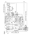
- the data transfer system comprises a plurality of, two in the illustrated embodiment, FDDs 10 and 10' daisy chained to host equipment 12 composed of a CPU 14 and a controller 16.
- the CPU 14 is well known in the art.
- the controller 16 is also a standard component of this type of data transfer system, functioning to deliver and receive signals to and from the FDDs 10 and 10' in a manner more fully set forth hereafter. Suffice it to say, therefore, that the controller 16 broadly comprises an interface for interaction with the CPU 14, a controller/for- matter section, and another interface for interaction with the FDDs 10 and 10'.
- the two FDDs 10 and 10' are of like construction. We will therefore describe only the first FDD 10 in detail, it being understood that the same description applies to the other FDD 10'.
- the representative FDD 10 is shown to have loaded therein a replaceable floppy disk cartridge 18 having a magnetic disk for rotation by an electric motor 20.
- the drive mechanism for imparting the rotation of this motor 20 to the magnetic disk nor the clamp mechanism for clamping the magnetic disk against the drive mechanism, as these mechanisms are per se well known in the art and do not constitute features of our invention.
- the disk cartridge 18 to be single sided, rather than double sided, with only one magnetic transducer head 22 disposed on one side thereof for data transfer.
- the transducer head 22 is mounted to a carriage 24 for movement more or less in a radial direction of the disk cartridge 18 for track to track accessing.
- another electric motor 26 of the bidirectional stepping type having, for example, four phase windings to be excited in a controlled sequence to cause stepwise rotation of the rotor.
- the disk motor 20 may directly drive the magnetic disk
- the head motor 26 must of course be coupled to the head carriage 24 via a rotary to linear converter, not shown, which also is well known in the art.
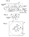
- FIG. 2 in order to explain a typical construction of the floppy disk cartridge 18 for use with the FDD 10. It has the aforesaid flexible magnetic disk 28 enclosed in a square envelope 30.
- This envelope has in each of its opposite surfaces a central aperture 32 larger than a concentric central aperture 34 in the disk 28, so that an annular portion 36 of the disk is exposed.
- the disk 28 is to have this exposed portion 36 clamped by the unshown clamp mechanism for rotation by the disk motor 20.
- the envelope 30 also has an elliptical opening 38 that serves to expose a radial portion of the disk 28.
- the transducer head 22 is to make data transfer contact with this exposed radial portion of the disk. Further a small hole 40 is formed through both surfaces of the envelope 30.
- an index hole 42 in the disk comes into register with the hole 40 at intervals and so allows passage of light or radiant energy to generate an electric pulse signal.
- a cutout 44 in a marginal edge of the envelope 30 is to be masked by the user against the passage of radiant energy if the disk 28 bears information that is not to be erased inadvertently.
- the disk motor 20 is connected to a disk motor control and drive circuit 46 to be controllably driven thereby.
- the disk motor control and drive circuit 46 includes feedback control means for holding the rotation of the disk motor 20 at a prescribed constant speed in response to an input signal representative of the actual speed of the disk motor, and drive means for energizing the disk motor under the control of the feedback control means.
- the disk motor control and drive circuit 46 is connected via an interface 48 to the controller 16 of the host equipment 12 to receive therefrom the standard MOTOR ON signal by way of a line 50.
- the line 50 has a branch line 50' connected to the second FDD 10'.
- the MOTOR ON signal is common to all the daisy chained FDDs and has heretofore been used to set all the disk motors into and out of rotation simultaneously. According to our invention, however, the disk motor of each FDD does not directly respond to the MOTOR ON signal, as will be more fully explained presently.
- the head motor 26 is connected to a head motor drive circuit 52 to be controllably driven thereby. If the head motor 26 is a four phase stepping motor, as we have assumed above, then the head motor drive circuit 52 may comprise four switching transistors for selectively energizing the four sets of windings of the head motor.
- the head motor drive circuit 52 is itself under the control of a transducer position control circuit 54 herein shown to comprise a head motor control circuit 56 and an up/down counter 58.
- the head motor control circuit 56 functions to deliver four phase drive control signals to the head motor drive circuit 52 so as to cause therethrough the bidirectiona, incremental rotation of the head motor 26 in a desired manner.
- the up/down counter 58 is connected via the interface 48 to the controller 16 to receive therefrom a DIRECTION SELECT signal and a STEP signal by way of lines 60 and 62 respectively.
- the DIRECTION SELECT signal determines the direction in which the transducer head 22 is to be moved by the head motor 26, that is, either radially inward or outward of the disk cartridge 18.
- the STEP signal represents the extent (the number of tracks) to which the transducer head 22 is to be moved in either direction.
- the up/down counter 58 responds to these input signals by delivering a corresponding output to the head motor control circuit 56, which in turn generates the noted four phase drive control signals accordingly for application to the head motor drive circuit 52.
- the transducer head 22 is connected to a read/write circuit 64.
- the read/write circuit 64 functions to direct the data read by the transducer head 22 to the controller 16 via the interface 48 and a line 66, and to send the data to be written, delivered from the controller by way of a line 68, on to the transducer head.
- the read/write circuit 64 is further connected via the interface 48 to the controller 16 by way of another line 70 to input a DRIVE SELECT signal.
- the DRIVE SELECT signal controls the passage of the outgoing and incoming data through the read/write circuit 64 in a manner that will become apparent from the following description of FIG. 3.
- FIG. 3 is a more detailed, although still somewhat schematic, illustration of the read/write circuit 64. Included in this circuit is a pulse shaper 72 connected to the transducer head 22 via a read amplifier 74. The data recovered from the disk cartridge by the transducer head 22 is amplified by the read amplifier 74, and the amplified replica of the recovered data enters the pulse shaper 72 thereby to be shaped into a form suitable for further processing. Connected downstream of the pulse shaper 72 is an AND type OR gate 76, having another input connected to receive the DRIVE SELECT signal from the controller ouput line 70 via the interface 48. The output of this OR gate is connected via the interface 48 to the controller input line 66.
- OR gate 76 allows the passage of the recovered data therethrough, toward the controller 16, only when the DRIVE SELECT signal is low.
- the OR gate 76 may therefore be called a data select gate.
- the read/write circuit 64 also included in the read/write circuit 64 is another data select gate in the form of an AND type NOR gate 78 designed to control the passage through the citcuit 64 of data to be written on the disk cartridge 24.
- the NOR gate 78 has three inputs, one for receiving the DRIVE SELECT signal from the controller 16 by way of its output line 70, another input for receiving a WRITE GATE signal from the controller 16, and still another for receiving an internally generated FILE PROTECT signal.
- the WRITE GATE signal goes low when the data already written on the disk may be erased for the introduction of new data.
- the FILE PROTECT signal goes high when the cutout 44, FIG. 2, in the disk cartridge envelope 30 is masked against the passage of radiant energy to inhibit the erasure of the recorded data.
- the output of the NOR gate 78 is connected to a write current supply circuit 80, to which there is also connected via the interface 48 the controller output line 68 for the delivery of the data to be written.
- the output of the write current supply circuit 80 is connected directly to the transducer head 22.
- the output from the NOR gate 78 goes high when its three input signals, the DRIVE SELECT signal, WRITE GATE signal, and FILE PROTECT signal, all go low. This high output enables the write current supply circuit 80 to deliver a write current, representative of the desired data to be written on the disk, to the transducer head 22.
- an index sensor assembly for sensing the angular position of the magnetic disk 28, FIG. 2, from the index hole 42 moving into and out of register with the hole 40 in the disk envelope 30.
- a disk sensor assembly 84 senses the presence or absence of the disk cartridge 18 in a preassigned data transfer position within the FDD.
- a head sensor assembly 86 senses from the position of the head carriage 24 the position of the transducer head 22 in the radial direction of the magnetic disk.
- the index sensor assembly 82, disk sensor assembly 84, and head sensor assembly 86 can all be conventional photoelectric sensing assemblies, each comprising a light source such as a light emitting diode and a photosensor such as a phototransistor.
- the three sensor assemblies 82, 84 and 86 named above are all electrically connected to a sensor control circuit 88.
- this sensor control circuit is the supply of electric current to the light sources of the sensor assemblies 82, 84 and 86.
- the sensor control circuit 88 further responds to the electric outputs from the photosensors of the sensor assemblies 82, 84 and 86 by producing an index signal, disk presence signal, and head position signal.
- the index signal and disk presence signal indicative respectively of the angular position of the magnetic disk and of the presence or absence of the disk cartridge in the data transfer position, are both delivered to a "ready" circuit 90 by way of lines 92 and 94.
- the head position signal representative of the radial position of the transducer head 22 on the magnetic disk, is applied to the up/down counter 58 of the transducer position control circuit 54 by way of a line 96.
- a "file protect" sensor assembly is assumed to be provided in the vicinity of the data transfer position of the disk cartridge 18. As the name implies, the "file protect” sensor assembly senses from the cutout 44, FIG. 2, in the disk cartridge envelope 30 whether data may be written on the disk or not. The output from the "file protect" sensor assembly is utilized as above stated for controlling the operation of the read/write circuit 64 as the FILE PROTECT signal.
- the "ready" circuit 90 determines, from the index signal and disk presence signal fed from the sensor control circuit 88, whether or not the magnetic disk is ready for the commencement of writing or reading.
- a READY output signal of the circuit 90 conveying this information, is directed via the interface 48 to the controller 16 by way of a line 98.
- the reference numeral 100 in FIG. 1 denotes a power control switch constituting a feature of our invention.
- the powr control switch 100 is connected between an external power line 102 conducting electric power to the FDD 10 and an internal power line 104 leading to some selected component or components of the FDD.
- the power control switch 100 further has an actuating signal line 106 connected to the controller output line 70 via the interface 48, in order to be turned on and off by the DRIVE SELECT signal.
- the external power line 102 Connected to a supply circuit, not shown, serving the complete data transfer system, the external power line 102 applies a prescribed working voltage to the FDD 10 when the power switch, also not shown, of the system is turned on.
- the internal power line 104 connected to the disk motor control and drive circuit 46, head motor drive circuit 52, read/write circuit 64, sensor control circuit 88, and "ready" circuit 90. All these circuits 46, 52, 64, 88 and 90 are therefore powered on and off by the power control switch 100. It will also be noted that the external power line 102 is connected directly to the interface 48 and to the head motor control circuit 56 and up/down counter 58 of the head position control circuit 54. These circuits 48, 56 and 58 are therefore unaffected by the power control switch 100.
- FIG. 4 shows an example of construction the power control switch 100 may take in practice.
- a switching transistor 108 is connected between external power line 102 and internal power line 104.
- another transistor 110 is connected between the base of the first recited transistor and ground.
- the second transistor 110 has its base connected to the signal line 106 to be actuated by the DRIVE SELECT signal.
- the power control switch 100 must close when the DRIVE SELECT signal is low in the illustrated embodiment.
- a NOT circuit 112 which functions to invert the DRIVE SELECT signal before its application to the second transistor 110.
- the second transistor 110 becomes conductive and so causes conduction through the first transistor 108 for the application of the supply voltage to the circuits 46, 52, 64, 88 and 90.
- the construction of the first FDD 10 which is interfaced with the controller 16 via the signal lines 50, 60, 62, 66, 68, 70 and 90.
- An additional line not shown, connects the controller 16 to the FDD 10 for the delivery of the noted WRITE GATE signal to the NOR gate 78, FIG. 3, of the read/write circuit 64.
- the data transfer system of this type usually has still another line, also not shown, for the delivery of an IN USE signal to each FDD, the IN USE signal being indicative of the fact that the FDD is in use for data transfer.
- the second FDD 10' is likewise interfaced with the controller 16 via signal lines 50', 60', 62', 66', 68', 70', 90', etc., similar to those between first FDD 10 and controller 16.
- signal lines 50', 60', 62', 66', 68', 70', 90', etc. similar to those between first FDD 10 and controller 16.
- an external power line connected to the second FDD 10'.
- FIG. 1 We have further indicated in FIG. 1 the lines where the waveforms of FIG. 5 appear, by the associated letters (A) through (E). Reference may therefore be had to both FIGS. 1 and 5, unless otherwise notified, for a better understanding of the operational description.
- the external power line 102 conducts power to the first FDD 10, as at (A) in FIG. 5, as the unshown power switch of the data transfer system is closed after the disk cartridge 18 has been loaded in the FDD and clamped in position therein.
- the power control switch 100 in accordance with our invention is held open, the supply voltage will be impressed only to the interface 48, head motor control circuit 56 and up/down counter 58 of the FDD 10, and not to the disk motor control and drive circuit 46, head motor drive circuit 52, read/write circuit 64, sensor control circuit 88, and "ready" circuit 90.
- the transducer head 22 must be returned to the "track zero" position on the magnetic disk of the loaded disk cartridge 18 upon closure of the system power switch. To make this possible the DRIVE SELECT signal goes low and is held in that state for a certain length of time, with the consequent closure of the power control switch 100 during the same length of time. As the transducer head 22 returns to track zero, through the procedure that is routine in this type of apparatus, the sensor control circuit 88 senses that position of the transducer head from the output from the head sensor assembly 86 and further operates to reset the up/down counter 58 of the head position control circuit 54 via the line 96. The DRIVE SELECT signal goes high following the return of the transducer head 22 to the "track zero" position and the subsequent resetting of the up/down counter 58.
- the MOTOR ON signal is shown to go low at a moment tl.
- This signal is common to all the daisy chained FDDs 10 and 10'.
- the disk motors 20 of all the FDDs have simultaneously set into rotation when the MOTOR ON signal goes low.
- our invention does not yet allow the rotation of the disk motors, as the DRIVE SELECT signals for the FDDs 10 and 10' are both still held high as at (C) and (D) in FIG. 5.
- the power control switch 100 of the FDD 10 for example, remains open to hold the disk motor control and drive circuit 46 deenergized.
- the power control switch 100 When the DRIVE SELECT signal for the first FDD 10 goes low at a subsequent moment t2, the power control switch 100 becomes closed to allow energization of the disk motor drive and control circuit 46 by way of the internal power line 104, as at (E) in FIG. 5. Thereupon the disk motor 20 starts rotation as dicated by the MOTOR ON signal from the controller 16. The closure of the power control switch 100 results also in the energization of the head motor drive circuit 52, read/write circuit 64, sensor control circuit 88, and "ready" circuit 90.
- the DRIVE SELECT output line 70 of the controller 16 is further connected to the outgoing data select gate 76 and incoming data select gate 78 of the read/write circuit 64.
- the outgoing data select gate 76 becomes conditioned to allow the passage of the recovered data.
- the incoming data select gate 78 also becomes conditioned to allow the passage of the data to be written, provided that the WRITE GATE signal and FILE PROTECT signal are both low.
- the first DRIVE SELECT signal is held low as at (C) in FIG. 5 to allow energization of all the constituent circuits of the first FDD 10, reading or writing is possible in the same way as heretofore.
- the second DRIVE SELECT signal is shown to go low at a moment t4, immediately following the moment t3 when the first DRIVE SELECT signal goes high, as at (D) in FIG. 5. Accordingly, even though the common MOTOR ON signal has been held low from the moment tl, the power control switch of the second FDD 10' has remained open until the moment t4. This will realize a very substantial saving of power.
- the second DRIVE SELECT signal is shown to go high at a moment t5 upon completion of data transfer in the second FDD 10'.
- the first DRIVE SELECT signal is shown to remain high from the moment t3 to a moment t6, the latter moment following the moment t5 when the second DRIVE SELECT signal goes high.
- the power control switch 100 of the first FDD 10 is held open during this period, as at (E) in FIG. 5, so that the disk motor 20 is held out of rotation in the face of the sustained low state of the MOTOR ON signal as at (B) in FIG. 5.
- the circuits 46, 52, 64, 88 and 90 are also held unenergized. A saving of power is thus realized during the period from moment t3 to moment t6, too.
- the up/down counter 58 of the head position control circuit 54 has been held energized, being connected directly to the external power line 102, from moment t3 to moment t6.
- Such constant energization of the counter 58 enables the same to hold in storage the information representative of the angular position of the rotor of the head motor 26, or of the radial position of the transducer head 22 on the magnetic disk, at the moment t3 when the first DRIVE SELECT signal goes high. Consequently, when the first DRIVE SELECT signal goes low again at the moment t6, no recalibration of the head position is necessary, making possible the immediate recommencement of data transfer between disk and head.
- the first DRIVE SELECT signal is shown to go high at a moment t7, as at (C) in FIG. 5, with the consequent opening of the power control switch 100 as at (E) in FIG. 5.
- the common MOTOR ON signal is shown to go high at a subsequent moment t8, as at (B) in FIG. 5, to complete a single run of operation of the daisy chained FDDs 10 and 10'.
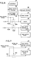
- FIG. 6 is shown our invention as adapted for a data transfer system having two separate external power lines 102a and 102a' for the application of different supply voltages to each FDD.
- the first power line 102a is intended for the application of a five volt supply voltage to the interface 48, head motor control circuit 56, counter 58, sensor control circuit 88, read/write circuit 64, and "ready" circuit 90.
- the second power line 102a' is intended for the application of a 12 volt supply voltage to the disk motor control and drive circuit 46 and head motor drive circuit 52.
- first power control switch 100a between the first power line 102a and the sensor control circuit 88, read/write circuit 64 and "ready" circuit 90, and of a second power control switch 100a' between the second power line 102a' and the disk motor control and drive circuit 46 and head motor drive circuit 52.
- the interface 48, head motor control circuit 56 and counter 58 are all connected directly to the first power line 102a.
- the two power control switches 100a and 100a' can each be constructed as in FIG. 4 and are to close in response to the low state of the DRIVE SELECT signal. The other details of construction and operation are substantially as set forth above in connection with FIGS. 1 through 5.
- FIG. 7 shows another slight modification of the FIG. 1 embodiment, wherein the disk motor drive and control circuit 46 is connected directly to the external power line 102 whereas the head motor drive circuit 52 is connected to the external power line via the power control switch 100.
- the disk motor drive and control circuit 46 drives the disk motor 20, FIG. 1, under the control of the MOTOR ON signal, regardless of whether the associated DRIVE SELECT signal is high or low.
- the head motor drive circuit 52 is powered only when the DRIVE SELECT signal is low as in the FIG. 1 embodiment.
- the power control switch 100 is actuated not only by the DRIVE SELECT signal but also by an output from a timer 120 which in turn is responsive to an output from a "power on” sensor circuit 122.
- the "power on” sensor circuit 122 Connected to the external power line 102, the "power on” sensor circuit 122 triggers the timer 120 upon closure of the unshown power switch of the data transfer system.
- the output from the timer 120 goes low, for instance, on triggering and remains in that state for a predetermined length of time thereafter, resulting in the closure of the power control switch 100 during the same period.
- the head motor drive circuit 52 is powered immediately upon closure of the system power switch to enable the return of the transducer head to the "track zero" position on the magnetic disk.
- the timer output itself may also be used for the return of the transducer head to the initial position.
- FIG. 9 illustrates another preferred form of record medium that may be employed in substitution for the disk cartridge 18 of FIG. 2 with the data transfer apparatus of our invention.
- the alternative record medium also has a flexible magnetic disk 28a, with a diameter of approximately 3.5 inches (86 millimeters), housed in an envelope 130 which is molded of synthetic resin material and which has greater rigidity than the envelope 30 of the disk cartridge 18.
- the envelope 130 has a slot 132 formed in at least one side thereof to expose a radial portion of the disk 28a for data transfer with the transducer head.
- the slot 132 is normally closed by a slidable cover 134, itself having a slot 136 formed therein, on the envelope 130.
- the cover 134 is sprung and normally held in the illustrated position on the envelope 130, with the slot 136 therein out of register with the slot 132 in the cover. In use, then, the cover 134 is slid over the envelope 130 against the spring pressure to bring the slot 136 into register with the slot 132.
- the envelope 130 has further formed therein a central aperture 138 to expose a central portion of the magnetic disk 28a.
- This disk has a rigid hub 140 at its exposed central portion.
- the hub 140 is to be magnetically attached to a drive hub, not shown, of the data transfer apparatus.
- the hub 140 has formed therein a central square opening 142 and an eccentric elliptical opening 144 for the insertion of a spindle and drive pin, both not shown, of the data transfer apparatus.
- the sensor control circuit 88 might be connected directly to the power supply, instead of via the power control switch 100 or 100a as in the FIG. 1 or 6 embodiment. Further the head motor control circuit 56, counter 58 might be connected to the power supply via the power control switch 100.
- any desired one or more of the pertinent components of the data transfer apparatus may be connected to the power supply via the power control switch. It is therefore appropriate that our invention be construed broadly and in a manner consistent with the fair meaning or proper scope of the following claims.
Landscapes
- Signal Processing For Digital Recording And Reproducing (AREA)
- Moving Of Heads (AREA)
- Moving Of Head For Track Selection And Changing (AREA)
- Rotational Drive Of Disk (AREA)
Abstract
Description
- Our invention relates to apparatus employing disklike record media for the recording and/or reproduction of data, and more specifically to apparatus for data transfer with flexible magnetic disks now commonly referred to as floppy disks, although we do not wish our invention to be unnecessarily limited to this particular type of record medium.
- Floppy disks have found widespread acceptance in information processing and allied industries, as well as in offices in general, as compact data storage media. Being thin and limply flexible, the disks are usually encased in more rigid, apertured envelopes to make up disk assemblies or cartridges that are self supporting. There have also been suggested and used a variety of devices, known as floppy disk drives (FDDs), for data transfer to and from such disk cartridges. Dalziel et al. U.S. Patent 3,678,481 and Castrodale et al. U.S. Patent 4,089,029 represent examples of such known FDDs.
- FDDs are usually not self contained; they are subservient to host equipment typically comprising a central processor unit (CPU) and an associated controller. A familiar example of such mode of use is the daisy chaining of two or more FDDs to a CPU via a controller, with the FDDs in parallel relation to each other. Each FDD intended for use with host equipment has no power switch of its own. In a data transfer system comprising a CPU, a controller, and FDDs, for example, only one power switch serves the complete system. A problem has arisen in conjunction with this standardized power supply system. The FDDs are not necessarily used for data transfer at all times after the power switch of the complete system is turned on. Conventionally, however, power has been fed to the various components of the FDDs even when they are not in actual use. This of course has incurred a substantial waste of energy.
- We object to that waste of energy and hereby propose an improved data transfer apparatus that has realized a remarkable curtailment of power consumption in a simple and thoroughly practicable maner and without in any way sacrificing its operation.
- According to our invention, stated in its perhaps broadest aspect, there is provided a data transfer apparatus comprising a first motor controllably driven by a first drive circuit for imparting rotation to a disklike record medium, a second motor controllably driven by a second drive circuit for moving a transducer radially of the record medium in data transfer relation therewith, and a read/write circuit connected to the transducer and including at least one data select gate for controlling the passage therethrough of the data read from, or to be written on, the record medium. The data select gate is under the control of a drive select signal having two different prescribed states (high and low),- a first prescribed state (e.g. low) for causing the data select gate to pass the incoming or outgoing data and a second prescribed state (e.g. high) for causing the gate to block the data. At least one (preferably all) of the first and second drive circuits and the read/write circuit is connected to power supply means via power control switch means which is opened and closed by the drive select signal. The power control switch means closes when the drive select signal is in the first prescribed state, and opens when the drive select signal is in the second prescribed state.
- As will be understood, the apparatus need not perform data transfer between record medium and transducer when the drive select signal is in the second prescribed state and so conditions the data select gate to block the passage of data. Consequently, during each second prescribed state of the data select signal, the first and second drive circuits and the read/write circuit need not be powered as these circuits are normally required to operate only during the progress of actual data transfer. Any one or more of these circuits may therefore be connected to the power supply means via the power control switch means so as to be powered only when the data select gate is conditioned to pass data by the drive select signal. Any other standard component of the apparatus that need not operate when the drive select signal is in the second prescribed state may likewise be connected to the power supply means via the power control switch means. Examples of such additional circuits that may be connected to the power control switch means are a sensor control circuit for sensing the angular position of the record medium, and a "ready" circuit responsive to an output from the sensor control circuit for sensing the fact that the record medium is ready for data transfer.
- Some components, however, should advantageously be powered even when the data select gate is conditioned to block the passage of data. Such components may be coupled directly to the power supply means. An example of such com- ponents is a transducer position control circuit for controlling the position of the transducer on the record medium, as the circuit includes a counter for constantly storing information indicative of the radial position of the transducer on the record medium. Another example is an interface unit if the apparatus is interfaced with host equipment.
- Our invention is disclosed herein as adapted for a multiple data transfer system having a plurality of FDDs interfaced with and daisy chained to a CPU via a controller. The controller delivers the drive select signals to the respective FDDs, each constructed as in the foregoing summary, for selective use of the record media loaded therein. The drive select signals have heretofore been used for that purpose, so that our invention requires no substantial alteration of the existing parts of FDDs, or of the complete system, other than the provision of the power control switch means and associated electrical connections to attain the objectives for which it is intended.
- The above and other features and advantages of our invention and the manner of realizing them will become more apparent, and the invention itself will best be understood, from a study of the following description and appended claims, with reference had to the attached drawings showing some preferable embodiments of the invention.
-
- FIG. 1 is a block diagram of the data transfer system embodying the principles of our invention, with the data transfer system comprising a plurality of daisy chained FDDs each having a flexible magnetic disk cartridge loaded therein for selective data transfer;
- FIG. 2 is a plan view of a typical form of the flexible magnetic disk cartridge for use with each FDD of the data transfer system of FIG. 1;
- FIG. 3 is a block diagram showing in greater detail the read/write circuit in each FDD of the data transfer system of FIG. 1;
- FIG. 4 is a schematic electrical diagram showing in detail a practical example of the power control switch build into each FDD of the FIG. 1 system in accordance with our invention;
- FIG. 5 is a diagram plotting the waveforms appearing in various parts of the FIG. 1 system, as well as the states of the power lines of that system, the diagram being useful in explaining the operation of the data transfer system;
- FIG. 6 is a block diagram showing part of a slight modification of each FDD of the FIG. 1 system;
- FIG. 7 is also a block diagram showing part of another slight modification of each FDD of the FIG. 1 system;
- FIG. 8 is also a block diagram showing part of still another still modification of each FDD of the FIG. 1 system; and
- FIG. 9 is a plan view of another example of record medium suitable for use with the data transfer apparatus of our invention.
- We have illustrated in FIG. 1 the multiple data transfer system which, we believe, represents the best mode of carrying out our invention. The data transfer system comprises a plurality of, two in the illustrated embodiment,
FDDs 10 and 10' daisy chained tohost equipment 12 composed of aCPU 14 and acontroller 16. TheCPU 14 is well known in the art. Thecontroller 16 is also a standard component of this type of data transfer system, functioning to deliver and receive signals to and from theFDDs 10 and 10' in a manner more fully set forth hereafter. Suffice it to say, therefore, that thecontroller 16 broadly comprises an interface for interaction with theCPU 14, a controller/for- matter section, and another interface for interaction with theFDDs 10 and 10'. - The two
FDDs 10 and 10' are of like construction. We will therefore describe only thefirst FDD 10 in detail, it being understood that the same description applies to the other FDD 10'. - The representative FDD 10 is shown to have loaded therein a replaceable
floppy disk cartridge 18 having a magnetic disk for rotation by anelectric motor 20. We have not illustrated the drive mechanism for imparting the rotation of thismotor 20 to the magnetic disk, nor the clamp mechanism for clamping the magnetic disk against the drive mechanism, as these mechanisms are per se well known in the art and do not constitute features of our invention. Further, in order to facilitate description, we have shown thedisk cartridge 18 to be single sided, rather than double sided, with only onemagnetic transducer head 22 disposed on one side thereof for data transfer. Thetransducer head 22 is mounted to acarriage 24 for movement more or less in a radial direction of thedisk cartridge 18 for track to track accessing. Employed for such radial travel of the transducer head is another electric motor 26 of the bidirectional stepping type having, for example, four phase windings to be excited in a controlled sequence to cause stepwise rotation of the rotor. - We will hereinafter referr to the first recited
motor 20 as the disk motor, and to the second motor 26 as the head motor, by way of contradistinction from each other. While thedisk motor 20 may directly drive the magnetic disk, the head motor 26 must of course be coupled to thehead carriage 24 via a rotary to linear converter, not shown, which also is well known in the art. - Reference is now directed to FIG. 2 in order to explain a typical construction of the
floppy disk cartridge 18 for use with the FDD 10. It has the aforesaid flexiblemagnetic disk 28 enclosed in asquare envelope 30. This envelope has in each of its opposite surfaces acentral aperture 32 larger than a concentriccentral aperture 34 in thedisk 28, so that anannular portion 36 of the disk is exposed. Thedisk 28 is to have this exposedportion 36 clamped by the unshown clamp mechanism for rotation by thedisk motor 20. Theenvelope 30 also has anelliptical opening 38 that serves to expose a radial portion of thedisk 28. Thetransducer head 22 is to make data transfer contact with this exposed radial portion of the disk. Further asmall hole 40 is formed through both surfaces of theenvelope 30. When thedisk 28 rotates within theenvelope 30, anindex hole 42 in the disk comes into register with thehole 40 at intervals and so allows passage of light or radiant energy to generate an electric pulse signal. Acutout 44 in a marginal edge of theenvelope 30 is to be masked by the user against the passage of radiant energy if thedisk 28 bears information that is not to be erased inadvertently. - With reference back to FIG. 1 the
disk motor 20 is connected to a disk motor control and drivecircuit 46 to be controllably driven thereby. The disk motor control and drivecircuit 46 includes feedback control means for holding the rotation of thedisk motor 20 at a prescribed constant speed in response to an input signal representative of the actual speed of the disk motor, and drive means for energizing the disk motor under the control of the feedback control means. - Further the disk motor control and drive
circuit 46 is connected via aninterface 48 to thecontroller 16 of thehost equipment 12 to receive therefrom the standard MOTOR ON signal by way of aline 50. It will be seen that theline 50 has a branch line 50' connected to the second FDD 10'. Thus the MOTOR ON signal is common to all the daisy chained FDDs and has heretofore been used to set all the disk motors into and out of rotation simultaneously. According to our invention, however, the disk motor of each FDD does not directly respond to the MOTOR ON signal, as will be more fully explained presently. - The head motor 26 is connected to a head
motor drive circuit 52 to be controllably driven thereby. If the head motor 26 is a four phase stepping motor, as we have assumed above, then the headmotor drive circuit 52 may comprise four switching transistors for selectively energizing the four sets of windings of the head motor. - The head
motor drive circuit 52 is itself under the control of a transducerposition control circuit 54 herein shown to comprise a headmotor control circuit 56 and an up/downcounter 58. The headmotor control circuit 56 functions to deliver four phase drive control signals to the headmotor drive circuit 52 so as to cause therethrough the bidirectiona, incremental rotation of the head motor 26 in a desired manner. The up/downcounter 58 is connected via theinterface 48 to thecontroller 16 to receive therefrom a DIRECTION SELECT signal and a STEP signal by way oflines transducer head 22 is to be moved by the head motor 26, that is, either radially inward or outward of thedisk cartridge 18. The STEP signal represents the extent (the number of tracks) to which thetransducer head 22 is to be moved in either direction. The up/downcounter 58 responds to these input signals by delivering a corresponding output to the headmotor control circuit 56, which in turn generates the noted four phase drive control signals accordingly for application to the headmotor drive circuit 52. - The
transducer head 22 is connected to a read/write circuit 64. As the present data transfer system is equipped for both introduction and recovery of data to and from the disk cartridges, the read/write circuit 64 functions to direct the data read by thetransducer head 22 to thecontroller 16 via theinterface 48 and aline 66, and to send the data to be written, delivered from the controller by way of aline 68, on to the transducer head. The read/write circuit 64 is further connected via theinterface 48 to thecontroller 16 by way of anotherline 70 to input a DRIVE SELECT signal. The DRIVE SELECT signal controls the passage of the outgoing and incoming data through the read/write circuit 64 in a manner that will become apparent from the following description of FIG. 3. - FIG. 3 is a more detailed, although still somewhat schematic, illustration of the read/
write circuit 64. Included in this circuit is apulse shaper 72 connected to thetransducer head 22 via aread amplifier 74. The data recovered from the disk cartridge by thetransducer head 22 is amplified by theread amplifier 74, and the amplified replica of the recovered data enters thepulse shaper 72 thereby to be shaped into a form suitable for further processing. Connected downstream of thepulse shaper 72 is an AND type ORgate 76, having another input connected to receive the DRIVE SELECT signal from thecontroller ouput line 70 via theinterface 48. The output of this OR gate is connected via theinterface 48 to thecontroller input line 66. - Consequently the
OR gate 76 allows the passage of the recovered data therethrough, toward thecontroller 16, only when the DRIVE SELECT signal is low. TheOR gate 76 may therefore be called a data select gate. - Also included in the read/
write circuit 64 is another data select gate in the form of an AND type NORgate 78 designed to control the passage through thecitcuit 64 of data to be written on thedisk cartridge 24. The NORgate 78 has three inputs, one for receiving the DRIVE SELECT signal from thecontroller 16 by way of itsoutput line 70, another input for receiving a WRITE GATE signal from thecontroller 16, and still another for receiving an internally generated FILE PROTECT signal. The WRITE GATE signal goes low when the data already written on the disk may be erased for the introduction of new data. The FILE PROTECT signal, on the other hand, goes high when thecutout 44, FIG. 2, in thedisk cartridge envelope 30 is masked against the passage of radiant energy to inhibit the erasure of the recorded data. The output of the NORgate 78 is connected to a writecurrent supply circuit 80, to which there is also connected via theinterface 48 thecontroller output line 68 for the delivery of the data to be written. The output of the writecurrent supply circuit 80 is connected directly to thetransducer head 22. - Thus the output from the NOR
gate 78 goes high when its three input signals, the DRIVE SELECT signal, WRITE GATE signal, and FILE PROTECT signal, all go low. This high output enables the writecurrent supply circuit 80 to deliver a write current, representative of the desired data to be written on the disk, to thetransducer head 22. - Referring again to FIG. 1, we will now describe several sensor assemblies and associated circuit means included in the
FDD 10. At 82 is shown an index sensor assembly for sensing the angular position of themagnetic disk 28, FIG. 2, from theindex hole 42 moving into and out of register with thehole 40 in thedisk envelope 30. Adisk sensor assembly 84 senses the presence or absence of thedisk cartridge 18 in a preassigned data transfer position within the FDD. Ahead sensor assembly 86 senses from the position of thehead carriage 24 the position of thetransducer head 22 in the radial direction of the magnetic disk. Theindex sensor assembly 82,disk sensor assembly 84, andhead sensor assembly 86 can all be conventional photoelectric sensing assemblies, each comprising a light source such as a light emitting diode and a photosensor such as a phototransistor. - The three
sensor assemblies sensor control circuit 88. Among the functions of this sensor control circuit is the supply of electric current to the light sources of thesensor assemblies sensor control circuit 88 further responds to the electric outputs from the photosensors of thesensor assemblies circuit 90 by way oflines transducer head 22 on the magnetic disk, is applied to the up/down counter 58 of the transducerposition control circuit 54 by way of aline 96. Although not illustrated, a "file protect" sensor assembly is assumed to be provided in the vicinity of the data transfer position of thedisk cartridge 18. As the name implies, the "file protect" sensor assembly senses from thecutout 44, FIG. 2, in thedisk cartridge envelope 30 whether data may be written on the disk or not. The output from the "file protect" sensor assembly is utilized as above stated for controlling the operation of the read/write circuit 64 as the FILE PROTECT signal. - The "ready"
circuit 90 determines, from the index signal and disk presence signal fed from thesensor control circuit 88, whether or not the magnetic disk is ready for the commencement of writing or reading. A READY output signal of thecircuit 90, conveying this information, is directed via theinterface 48 to thecontroller 16 by way of aline 98. - The
reference numeral 100 in FIG. 1 denotes a power control switch constituting a feature of our invention. Thepowr control switch 100 is connected between anexternal power line 102 conducting electric power to theFDD 10 and aninternal power line 104 leading to some selected component or components of the FDD. Thepower control switch 100 further has anactuating signal line 106 connected to thecontroller output line 70 via theinterface 48, in order to be turned on and off by the DRIVE SELECT signal. Connected to a supply circuit, not shown, serving the complete data transfer system, theexternal power line 102 applies a prescribed working voltage to theFDD 10 when the power switch, also not shown, of the system is turned on. We have herein shown theinternal power line 104 connected to the disk motor control and drivecircuit 46, headmotor drive circuit 52, read/writecircuit 64,sensor control circuit 88, and "ready"circuit 90. All thesecircuits power control switch 100. It will also be noted that theexternal power line 102 is connected directly to theinterface 48 and to the headmotor control circuit 56 and up/down counter 58 of the headposition control circuit 54. Thesecircuits power control switch 100. - FIG. 4 shows an example of construction the
power control switch 100 may take in practice. A switchingtransistor 108 is connected betweenexternal power line 102 andinternal power line 104. For the on/off control of thistransistor 108 another transistor 110 is connected between the base of the first recited transistor and ground. The second transistor 110 has its base connected to thesignal line 106 to be actuated by the DRIVE SELECT signal. Thepower control switch 100 must close when the DRIVE SELECT signal is low in the illustrated embodiment. Employed to this end is aNOT circuit 112 which functions to invert the DRIVE SELECT signal before its application to the second transistor 110. Thus, whenever the DRIVE SELECT signal goes low, the second transistor 110 becomes conductive and so causes conduction through thefirst transistor 108 for the application of the supply voltage to thecircuits - We have so far described the construction of the
first FDD 10, which is interfaced with thecontroller 16 via the signal lines 50, 60, 62, 66, 68, 70 and 90. An additional line, not shown, connects thecontroller 16 to theFDD 10 for the delivery of the noted WRITE GATE signal to the NORgate 78, FIG. 3, of the read/write circuit 64. The data transfer system of this type usually has still another line, also not shown, for the delivery of an IN USE signal to each FDD, the IN USE signal being indicative of the fact that the FDD is in use for data transfer. - The second FDD 10' is likewise interfaced with the
controller 16 via signal lines 50', 60', 62', 66', 68', 70', 90', etc., similar to those betweenfirst FDD 10 andcontroller 16. At 102' is shown an external power line connected to the second FDD 10'. - In the following operational description of the data transfer system, configured as in the foregoing, we will refer to the waveform diagram of FIG. 5. Depicted in this figure are, from top to bottom:
- (A) The state of the
external power line 102 connected to thefirst FDD 10. - (B) The common MOTOR ON signal applied from the
controller 16 to the disk motor control and drivecircuits 46 of bothFDDs 10 and 10'. - (C) The first DRIVE SELECT signal applied from the controller to the read/
write circuit 64 andpower control switch 100 of thefirst FDD 10. - (D) The second DRIVE SELECT signal applied from the controller to the read/write circuit and power control switch of the second FDD 10'.
- (E) The state of the
internal power line 104 of thefirst FDD 10. - We have further indicated in FIG. 1 the lines where the waveforms of FIG. 5 appear, by the associated letters (A) through (E). Reference may therefore be had to both FIGS. 1 and 5, unless otherwise notified, for a better understanding of the operational description.
- The
external power line 102 conducts power to thefirst FDD 10, as at (A) in FIG. 5, as the unshown power switch of the data transfer system is closed after thedisk cartridge 18 has been loaded in the FDD and clamped in position therein. However, as long as thepower control switch 100 in accordance with our invention is held open, the supply voltage will be impressed only to theinterface 48, headmotor control circuit 56 and up/down counter 58 of theFDD 10, and not to the disk motor control and drivecircuit 46, headmotor drive circuit 52, read/writecircuit 64,sensor control circuit 88, and "ready"circuit 90. - The
transducer head 22 must be returned to the "track zero" position on the magnetic disk of the loadeddisk cartridge 18 upon closure of the system power switch. To make this possible the DRIVE SELECT signal goes low and is held in that state for a certain length of time, with the consequent closure of thepower control switch 100 during the same length of time. As thetransducer head 22 returns to track zero, through the procedure that is routine in this type of apparatus, thesensor control circuit 88 senses that position of the transducer head from the output from thehead sensor assembly 86 and further operates to reset the up/down counter 58 of the headposition control circuit 54 via theline 96. The DRIVE SELECT signal goes high following the return of thetransducer head 22 to the "track zero" position and the subsequent resetting of the up/downcounter 58. - Thereafter, as at (B) in FIG. 5, the MOTOR ON signal is shown to go low at a moment tl. This signal is common to all the daisy chained FDDs 10 and 10'. Conventionally, therefore, the
disk motors 20 of all the FDDs have simultaneously set into rotation when the MOTOR ON signal goes low. However, our invention does not yet allow the rotation of the disk motors, as the DRIVE SELECT signals for the FDDs 10 and 10' are both still held high as at (C) and (D) in FIG. 5. Thepower control switch 100 of theFDD 10, for example, remains open to hold the disk motor control and drivecircuit 46 deenergized. - When the DRIVE SELECT signal for the
first FDD 10 goes low at a subsequent moment t2, thepower control switch 100 becomes closed to allow energization of the disk motor drive andcontrol circuit 46 by way of theinternal power line 104, as at (E) in FIG. 5. Thereupon thedisk motor 20 starts rotation as dicated by the MOTOR ON signal from thecontroller 16. The closure of thepower control switch 100 results also in the energization of the headmotor drive circuit 52, read/writecircuit 64,sensor control circuit 88, and "ready"circuit 90. - As has been stated with reference to FIG. 3, the DRIVE
SELECT output line 70 of thecontroller 16 is further connected to the outgoing data selectgate 76 and incoming data selectgate 78 of the read/write circuit 64. When the DRIVE SELECT signal goes low as above, the outgoing data selectgate 76 becomes conditioned to allow the passage of the recovered data. The incoming data selectgate 78 also becomes conditioned to allow the passage of the data to be written, provided that the WRITE GATE signal and FILE PROTECT signal are both low. Thus, during the period from moment t2 to moment t3, when the first DRIVE SELECT signal is held low as at (C) in FIG. 5 to allow energization of all the constituent circuits of thefirst FDD 10, reading or writing is possible in the same way as heretofore. - The second DRIVE SELECT signal, on the other hand, is shown to go low at a moment t4, immediately following the moment t3 when the first DRIVE SELECT signal goes high, as at (D) in FIG. 5. Accordingly, even though the common MOTOR ON signal has been held low from the moment tl, the power control switch of the second FDD 10' has remained open until the moment t4. This will realize a very substantial saving of power. The second DRIVE SELECT signal is shown to go high at a moment t5 upon completion of data transfer in the second FDD 10'.
- The first DRIVE SELECT signal is shown to remain high from the moment t3 to a moment t6, the latter moment following the moment t5 when the second DRIVE SELECT signal goes high. The
power control switch 100 of thefirst FDD 10 is held open during this period, as at (E) in FIG. 5, so that thedisk motor 20 is held out of rotation in the face of the sustained low state of the MOTOR ON signal as at (B) in FIG. 5. Thecircuits - It should be appreciated that the up/down counter 58 of the head
position control circuit 54 has been held energized, being connected directly to theexternal power line 102, from moment t3 to moment t6. Such constant energization of thecounter 58 enables the same to hold in storage the information representative of the angular position of the rotor of the head motor 26, or of the radial position of thetransducer head 22 on the magnetic disk, at the moment t3 when the first DRIVE SELECT signal goes high. Consequently, when the first DRIVE SELECT signal goes low again at the moment t6, no recalibration of the head position is necessary, making possible the immediate recommencement of data transfer between disk and head. The first DRIVE SELECT signal is shown to go high at a moment t7, as at (C) in FIG. 5, with the consequent opening of thepower control switch 100 as at (E) in FIG. 5. The common MOTOR ON signal is shown to go high at a subsequent moment t8, as at (B) in FIG. 5, to complete a single run of operation of the daisy chained FDDs 10 and 10'. - Although we have already set forth the advantatges gained by our invention, we may restudy in further detail the particular advantages of the illustrated data transfer system after having thus fully disclosed its construction and operation. The advantages are:
- 1. The power consumption of each FDD, while it is standing by for data transfer with the power switch of the complete system closed, can be reduced to approximately one third that of the prior art. This power saving capability manifests itself as an even greater advantage when the invention is applied to battery powered systems.
- 2. The
power control switch 100 does not require manual activation, nor is the provision of any particular switch activating means necessary other than thesigna line 106. - 3. Once the transducer head is returned to the "track zero" position on the magnetic disk when the system power switch is initially closed, the head position is constantly held in storage in the counter of the head position control circuit in spite of subsequent changes in the state of the DRIVE SELECT signal. Thus, whenever the DRIVE SELECT signal goes low, reading or writing can be recommenced with little or no delay. The information stored in the counter of the head position control circuit is used further for controlling the write current in accordance with the radial position of the transducer head on the magnetic disk, and for the selective use of the filter for the removal of the unncessary frequency component from the data being read out.
- In FIG. 6 is shown our invention as adapted for a data transfer system having two separate
external power lines first power line 102a is intended for the application of a five volt supply voltage to theinterface 48, headmotor control circuit 56, counter 58,sensor control circuit 88, read/writecircuit 64, and "ready"circuit 90. Thesecond power line 102a' is intended for the application of a 12 volt supply voltage to the disk motor control and drivecircuit 46 and headmotor drive circuit 52. - In this application we suggest the provision of a first
power control switch 100a between thefirst power line 102a and thesensor control circuit 88, read/writecircuit 64 and "ready"circuit 90, and of a secondpower control switch 100a' between thesecond power line 102a' and the disk motor control and drivecircuit 46 and headmotor drive circuit 52. As taught by the FIG. 1 embodiment, theinterface 48, headmotor control circuit 56 and counter 58 are all connected directly to thefirst power line 102a. The twopower control switches - FIG. 7 shows another slight modification of the FIG. 1 embodiment, wherein the disk motor drive and
control circuit 46 is connected directly to theexternal power line 102 whereas the headmotor drive circuit 52 is connected to the external power line via thepower control switch 100. Thus powered directly from theexternal power line 102, as has been the case heretofore, the disk motor drive andcontrol circuit 46 drives thedisk motor 20, FIG. 1, under the control of the MOTOR ON signal, regardless of whether the associated DRIVE SELECT signal is high or low. The headmotor drive circuit 52, on the other hand, is powered only when the DRIVE SELECT signal is low as in the FIG. 1 embodiment. - In still another modification of the FIG. 1 embodiment shown in FIG. 8, the
power control switch 100 is actuated not only by the DRIVE SELECT signal but also by an output from atimer 120 which in turn is responsive to an output from a "power on"sensor circuit 122. Connected to theexternal power line 102, the "power on"sensor circuit 122 triggers thetimer 120 upon closure of the unshown power switch of the data transfer system. The output from thetimer 120 goes low, for instance, on triggering and remains in that state for a predetermined length of time thereafter, resulting in the closure of thepower control switch 100 during the same period. - Connected to the
power control switch 100 in this case is at least the headmotor drive circuit 52 as, for example, in the FIG. 7 embodiment. The headmotor drive circuit 52 is powered immediately upon closure of the system power switch to enable the return of the transducer head to the "track zero" position on the magnetic disk. The timer output itself may also be used for the return of the transducer head to the initial position. - FIG. 9 illustrates another preferred form of record medium that may be employed in substitution for the
disk cartridge 18 of FIG. 2 with the data transfer apparatus of our invention. Generally designated 18a, the alternative record medium also has a flexiblemagnetic disk 28a, with a diameter of approximately 3.5 inches (86 millimeters), housed in anenvelope 130 which is molded of synthetic resin material and which has greater rigidity than theenvelope 30 of thedisk cartridge 18. Theenvelope 130 has aslot 132 formed in at least one side thereof to expose a radial portion of thedisk 28a for data transfer with the transducer head. Theslot 132 is normally closed by aslidable cover 134, itself having aslot 136 formed therein, on theenvelope 130. Thecover 134 is sprung and normally held in the illustrated position on theenvelope 130, with theslot 136 therein out of register with theslot 132 in the cover. In use, then, thecover 134 is slid over theenvelope 130 against the spring pressure to bring theslot 136 into register with theslot 132. - The
envelope 130 has further formed therein acentral aperture 138 to expose a central portion of themagnetic disk 28a. This disk has arigid hub 140 at its exposed central portion. In the form of a metal disk, thehub 140 is to be magnetically attached to a drive hub, not shown, of the data transfer apparatus. Thehub 140 has formed therein a centralsquare opening 142 and an eccentricelliptical opening 144 for the insertion of a spindle and drive pin, both not shown, of the data transfer apparatus. - Although we have shown and described our invention in terms of specific embodiments thereof and as adapted for a system having a plurality of daisy chained FDDs, it is understood that these are by way of example only and not to impose limitations upon the invention. A variety_of modifications or alterations will occur to one skilled in the art to conform to design preferences or to specific requirements of the applications of the invention. For example, the
sensor control circuit 88 might be connected directly to the power supply, instead of via thepower control switch motor control circuit 56, counter 58 might be connected to the power supply via thepower control switch 100. In short, according to the broadest aspect of our invention, any desired one or more of the pertinent components of the data transfer apparatus may be connected to the power supply via the power control switch. It is therefore appropriate that our invention be construed broadly and in a manner consistent with the fair meaning or proper scope of the following claims.
Claims (9)
and wherein the power control switch means comprises:
Applications Claiming Priority (2)
| Application Number | Priority Date | Filing Date | Title |
|---|---|---|---|
| JP139695/83 | 1983-07-29 | ||
| JP58139695A JPS6029968A (en) | 1983-07-29 | 1983-07-29 | Disk driver |
Publications (2)
| Publication Number | Publication Date |
|---|---|
| EP0133232A1 true EP0133232A1 (en) | 1985-02-20 |
| EP0133232B1 EP0133232B1 (en) | 1987-10-28 |
Family
ID=15251260
Family Applications (1)
| Application Number | Title | Priority Date | Filing Date |
|---|---|---|---|
| EP84108221A Expired EP0133232B1 (en) | 1983-07-29 | 1984-07-12 | Data transfer apparatus for use with a flexible magnetic disk or the like |
Country Status (4)
| Country | Link |
|---|---|
| EP (1) | EP0133232B1 (en) |
| JP (1) | JPS6029968A (en) |
| KR (1) | KR890004759B1 (en) |
| DE (1) | DE3467059D1 (en) |
Cited By (1)
| Publication number | Priority date | Publication date | Assignee | Title |
|---|---|---|---|---|
| EP0752783A3 (en) * | 1991-11-21 | 1997-11-19 | Canon Kabushiki Kaisha | Information signal processing apparatus |
Families Citing this family (2)
| Publication number | Priority date | Publication date | Assignee | Title |
|---|---|---|---|---|
| JPS62102472A (en) * | 1985-10-30 | 1987-05-12 | Oki Electric Ind Co Ltd | Magnetic disk device drive system |
| JPH0643893Y2 (en) * | 1987-04-09 | 1994-11-14 | 富士電機株式会社 | Built-in circuit start / stop controller for disk storage device |
Citations (3)
| Publication number | Priority date | Publication date | Assignee | Title |
|---|---|---|---|---|
| GB1432693A (en) * | 1972-07-24 | 1976-04-22 | Information Storage Systems | Entering data in data storage device |
| FR2458128A1 (en) * | 1979-05-31 | 1980-12-26 | Telecomm Electron Franc | Automatic switch-off for record player - senses absence of amplifier output to switch off motor and amplifier, and has motor to rotate disc |
| US4419701A (en) * | 1981-09-21 | 1983-12-06 | Quantum Corporation | Data transducer position control system for rotating disk data storage equipment |
-
1983
- 1983-07-29 JP JP58139695A patent/JPS6029968A/en active Pending
-
1984
- 1984-07-12 EP EP84108221A patent/EP0133232B1/en not_active Expired
- 1984-07-12 DE DE8484108221T patent/DE3467059D1/en not_active Expired
- 1984-07-30 KR KR1019840004520A patent/KR890004759B1/en not_active Expired
Patent Citations (3)
| Publication number | Priority date | Publication date | Assignee | Title |
|---|---|---|---|---|
| GB1432693A (en) * | 1972-07-24 | 1976-04-22 | Information Storage Systems | Entering data in data storage device |
| FR2458128A1 (en) * | 1979-05-31 | 1980-12-26 | Telecomm Electron Franc | Automatic switch-off for record player - senses absence of amplifier output to switch off motor and amplifier, and has motor to rotate disc |
| US4419701A (en) * | 1981-09-21 | 1983-12-06 | Quantum Corporation | Data transducer position control system for rotating disk data storage equipment |
Cited By (1)
| Publication number | Priority date | Publication date | Assignee | Title |
|---|---|---|---|---|
| EP0752783A3 (en) * | 1991-11-21 | 1997-11-19 | Canon Kabushiki Kaisha | Information signal processing apparatus |
Also Published As
| Publication number | Publication date |
|---|---|
| DE3467059D1 (en) | 1987-12-03 |
| KR890004759B1 (en) | 1989-11-25 |
| KR850001605A (en) | 1985-03-30 |
| JPS6029968A (en) | 1985-02-15 |
| EP0133232B1 (en) | 1987-10-28 |
Similar Documents
| Publication | Publication Date | Title |
|---|---|---|
| US4658307A (en) | Data transfer apparatus for use with a flexible magnetic disk or the like | |
| US4700243A (en) | Power saving circuit arrangement for an apparatus for data transfer with flexible magnetic disk or the like | |
| EP0110050A1 (en) | Disc drive for flexible discs with different track widths | |
| US4853799A (en) | Magnetic disk apparatus capable of writing at two different track densities | |
| US4688112A (en) | Power-saving data transfer apparatus with a flexible magnetic disk or the like | |
| EP0123849B1 (en) | Disk storage file with a four phase, single phase drive stepping motor | |
| JPH0222466B2 (en) | ||
| US4583133A (en) | Data transfer system with a plurality of disklike record media for selective use | |
| EP0133232B1 (en) | Data transfer apparatus for use with a flexible magnetic disk or the like | |
| GB2121230A (en) | Streaming cassette tape transport | |
| US4626942A (en) | Power-saving data transfer apparatus with a flexible magnetic disk or the like | |
| US5572383A (en) | Magnetic floppy disc drive receiving two discs having different sizes | |
| US5283702A (en) | Power saving system for rotating disk data storage apparatus | |
| US5400190A (en) | Power saving system for a disk sensor in rotating disk data storage apparatus | |
| US5303107A (en) | System for holding a track counter active despite power suspension in rotating disk data storage apparatus | |
| US4769724A (en) | Magnetic head drive apparatus which uses a common current source for the read/write head and the erasing head | |
| US4825309A (en) | Circuit arrangement for the selective suppression and nonsuppression of read output in magnetic disk apparatus | |
| US4870514A (en) | Disk drive circuit arrangement for the suppression of undesired index pulses | |
| US4524399A (en) | Magnetic disk memory power supply | |
| US5051850A (en) | Disc unit having a central control for control plural disc drives | |
| US5357384A (en) | Rotating disk data storage apparatus capable of preventing head travel when the disk is not loaded | |
| EP0371778A3 (en) | Automatic tracking apparatus | |
| US4914532A (en) | Method of efficiently erasing data in accordance with type of magnetic recording medium and apparatus for realizing the same | |
| EP0364355A3 (en) | Spindle servo control for electronic still camera | |
| JPH07225635A (en) | Information storage device |
Legal Events
| Date | Code | Title | Description |
|---|---|---|---|
| PUAI | Public reference made under article 153(3) epc to a published international application that has entered the european phase |
Free format text: ORIGINAL CODE: 0009012 |
|
| AK | Designated contracting states |
Designated state(s): CH DE FR GB LI NL SE |
|
| 17P | Request for examination filed |
Effective date: 19850418 |
|
| 17Q | First examination report despatched |
Effective date: 19860709 |
|
| GRAA | (expected) grant |
Free format text: ORIGINAL CODE: 0009210 |
|
| AK | Designated contracting states |
Kind code of ref document: B1 Designated state(s): CH DE FR GB LI NL SE |
|
| PG25 | Lapsed in a contracting state [announced via postgrant information from national office to epo] |
Ref country code: SE Free format text: THE PATENT HAS BEEN ANNULLED BY A DECISION OF A NATIONAL AUTHORITY Effective date: 19871028 Ref country code: NL Effective date: 19871028 Ref country code: LI Effective date: 19871028 Ref country code: FR Free format text: THE PATENT HAS BEEN ANNULLED BY A DECISION OF A NATIONAL AUTHORITY Effective date: 19871028 Ref country code: CH Effective date: 19871028 |
|
| REF | Corresponds to: |
Ref document number: 3467059 Country of ref document: DE Date of ref document: 19871203 |
|
| REG | Reference to a national code |
Ref country code: CH Ref legal event code: PL |
|
| EN | Fr: translation not filed | ||
| NLV1 | Nl: lapsed or annulled due to failure to fulfill the requirements of art. 29p and 29m of the patents act | ||
| PLBE | No opposition filed within time limit |
Free format text: ORIGINAL CODE: 0009261 |
|
| STAA | Information on the status of an ep patent application or granted ep patent |
Free format text: STATUS: NO OPPOSITION FILED WITHIN TIME LIMIT |
|
| 26N | No opposition filed | ||
| REG | Reference to a national code |
Ref country code: GB Ref legal event code: IF02 |
|
| PGFP | Annual fee paid to national office [announced via postgrant information from national office to epo] |
Ref country code: GB Payment date: 20030709 Year of fee payment: 20 |
|
| PGFP | Annual fee paid to national office [announced via postgrant information from national office to epo] |
Ref country code: DE Payment date: 20030724 Year of fee payment: 20 |
|
| PG25 | Lapsed in a contracting state [announced via postgrant information from national office to epo] |
Ref country code: GB Free format text: LAPSE BECAUSE OF EXPIRATION OF PROTECTION Effective date: 20040711 |
|
| REG | Reference to a national code |
Ref country code: GB Ref legal event code: PE20 |