EP0132025B1 - Heterostructure bipolar transistor - Google Patents
Heterostructure bipolar transistor Download PDFInfo
- Publication number
- EP0132025B1 EP0132025B1 EP84303235A EP84303235A EP0132025B1 EP 0132025 B1 EP0132025 B1 EP 0132025B1 EP 84303235 A EP84303235 A EP 84303235A EP 84303235 A EP84303235 A EP 84303235A EP 0132025 B1 EP0132025 B1 EP 0132025B1
- Authority
- EP
- European Patent Office
- Prior art keywords
- layer
- emitter
- base
- heterojunction
- base layer
- Prior art date
- Legal status (The legal status is an assumption and is not a legal conclusion. Google has not performed a legal analysis and makes no representation as to the accuracy of the status listed.)
- Expired
Links
- 239000012535 impurity Substances 0.000 claims description 43
- 229910001218 Gallium arsenide Inorganic materials 0.000 claims description 33
- 239000000463 material Substances 0.000 claims description 9
- 239000004065 semiconductor Substances 0.000 claims description 6
- 230000005684 electric field Effects 0.000 description 24
- 238000000034 method Methods 0.000 description 18
- 239000000758 substrate Substances 0.000 description 13
- 238000009826 distribution Methods 0.000 description 9
- 230000015556 catabolic process Effects 0.000 description 8
- 239000000969 carrier Substances 0.000 description 4
- 238000004519 manufacturing process Methods 0.000 description 4
- 238000005229 chemical vapour deposition Methods 0.000 description 3
- 230000000694 effects Effects 0.000 description 3
- 230000008030 elimination Effects 0.000 description 3
- 238000003379 elimination reaction Methods 0.000 description 3
- 238000001451 molecular beam epitaxy Methods 0.000 description 3
- 230000002093 peripheral effect Effects 0.000 description 3
- 230000005641 tunneling Effects 0.000 description 3
- 238000002347 injection Methods 0.000 description 2
- 239000007924 injection Substances 0.000 description 2
- 230000003247 decreasing effect Effects 0.000 description 1
- 238000010586 diagram Methods 0.000 description 1
- 238000009792 diffusion process Methods 0.000 description 1
- 238000005530 etching Methods 0.000 description 1
- 238000002474 experimental method Methods 0.000 description 1
- 238000003860 storage Methods 0.000 description 1
- 230000007704 transition Effects 0.000 description 1
Images

Classifications
-
- H—ELECTRICITY
- H01—ELECTRIC ELEMENTS
- H01L—SEMICONDUCTOR DEVICES NOT COVERED BY CLASS H10
- H01L29/00—Semiconductor devices adapted for rectifying, amplifying, oscillating or switching, or capacitors or resistors with at least one potential-jump barrier or surface barrier, e.g. PN junction depletion layer or carrier concentration layer; Details of semiconductor bodies or of electrodes thereof ; Multistep manufacturing processes therefor
- H01L29/66—Types of semiconductor device ; Multistep manufacturing processes therefor
- H01L29/68—Types of semiconductor device ; Multistep manufacturing processes therefor controllable by only the electric current supplied, or only the electric potential applied, to an electrode which does not carry the current to be rectified, amplified or switched
- H01L29/70—Bipolar devices
- H01L29/72—Transistor-type devices, i.e. able to continuously respond to applied control signals
- H01L29/73—Bipolar junction transistors
- H01L29/737—Hetero-junction transistors
- H01L29/7371—Vertical transistors
-
- Y—GENERAL TAGGING OF NEW TECHNOLOGICAL DEVELOPMENTS; GENERAL TAGGING OF CROSS-SECTIONAL TECHNOLOGIES SPANNING OVER SEVERAL SECTIONS OF THE IPC; TECHNICAL SUBJECTS COVERED BY FORMER USPC CROSS-REFERENCE ART COLLECTIONS [XRACs] AND DIGESTS
- Y10—TECHNICAL SUBJECTS COVERED BY FORMER USPC
- Y10S—TECHNICAL SUBJECTS COVERED BY FORMER USPC CROSS-REFERENCE ART COLLECTIONS [XRACs] AND DIGESTS
- Y10S148/00—Metal treatment
- Y10S148/01—Bipolar transistors-ion implantation
-
- Y—GENERAL TAGGING OF NEW TECHNOLOGICAL DEVELOPMENTS; GENERAL TAGGING OF CROSS-SECTIONAL TECHNOLOGIES SPANNING OVER SEVERAL SECTIONS OF THE IPC; TECHNICAL SUBJECTS COVERED BY FORMER USPC CROSS-REFERENCE ART COLLECTIONS [XRACs] AND DIGESTS
- Y10—TECHNICAL SUBJECTS COVERED BY FORMER USPC
- Y10S—TECHNICAL SUBJECTS COVERED BY FORMER USPC CROSS-REFERENCE ART COLLECTIONS [XRACs] AND DIGESTS
- Y10S148/00—Metal treatment
- Y10S148/084—Ion implantation of compound devices
Definitions
- the present invention relates to a heterostructure bipolar transistor using a heterojunction as an emitter-base junction.
- a conventional bipolar transistor has an npn or pnp structure wherein emitter, base, and collector layers are made of a common semiconductor material. in this case, emitter and collector junctions are each a homojunction.
- Bipolar transistors using a heterojunction as the emitter junction and/or collector junction are receiving a great deal of attention and are being extensively studied these days.
- the heterojunction bipolar transistor has an advantage in that, when the emitter layer is made of a semiconductor material having a wider energy gap than that of the base layer, the emitter injection efficiency can be enhanced.
- the emitter junction is forward biased, carriers can be easily injected from the emitter to the base while carrier injection from the base to the emitter is limited due to an energy gap difference between the emitter and base layers. Therefore, the current gain of the heterostructure bipolar transistor becomes higher than that of the conventional homostructure type.
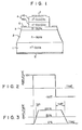
- Figure 1 shows the basic structure of conventional heterostructure bipolar transistors wherein a heterojunction is used as the emitter junction.
- This transistor comprises a GaAs-GaAIAs structure.
- An n-type GaAs collector layer 2, a p-type GaAs base layer 3, and an n-type Ga 1-x Al x As emitter layer 4 are sequentially deposited on an n +- type GaAs substrate 1.
- Reference numeral 5 denotes a collector electrode; 6, a base electrode; and 7, an emitter electrode.
- the emitter layer 4 comprises an n--type first emitter layer 4a which is in contact with the base layer 3, and an n + -type second emitter layer 4b which is in contact with the emitter electrode 7.
- a common feature of conventional heterostructure bipolar transistors is in that the first emitter layer 4a is thick.
- the structure in which the emitter layer comprises a two-layer structure of high- and low-impurity concentration layers and the first emitter layer is thick aims at decreasing the emitter junction capacitance so that the switching speed is increased (e.g., H. Kroemer "Heterostructure Bipolar Transistors and Integrated Circuits", Proc. IEEE, Vol. 70, No. 1, PP. 13-25, January 1982).
- the junction capacitance C JE can be expressed, in terms of an impurity concentration N E of the low-impurity concentration layer, as follows:
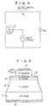
- the switching operation of transistors includes turn-on and turn-off.
- the propagation delay time tp d the average value of a turn-on time t on and a turn-off time toff, is taken as a reference of the switching speed.
- the turn-on time t on is defined to be a time for an output current to increase from 0% to 50%
- the turn-off time toff is defined to be a time for the output current to decrease from 100% to 50% (see Figure 3).
- the present inventors have made extensive studies of thicknesses of the respective layers and the relationship between the impurity concentration and the switching speed of the heterostructure bipolar transistor shown in Figure 1, by means of a numerical analysis model (e.g., M. Kurata "Principles of Operation of Bipolar Transistors", 1980, Kindai Kagaku-sha, and M. Kurata, "Numerical Analysis for Semiconductor Devices", 1982, Lexington Books, D. C. Heath and Company).
- M. Kurata Principal Analysis for Semiconductor Devices
- the first emitter layer has an impurity concentration N E of 3x10 16 cm -3 and a thickness W of 1 ⁇ m. Je and J c denote current densities of the emitter and the collector, respectively.
- the emitter and collector current densities must be set from 10 3 to 10 4 A/cm 2 or higher. This fact is apparent from various experiments and from analytical results using the numerical analysis model.
- the capability to inject carriers from the emitter to the base is smaller than that of type B.
- a high forward-bias voltage must be applied across the emitter-base junction. Under this operating condition, excess carriers are stored in the thick first emitter layer and the collector layer. As a result, the turn-off time is increased, and hence the propagation delay time is increased.
- the emitter junction capacitance C JE of type A is smaller than that of type B, but the switching speed of type A is lower than that of type B.
- type B is preferred to type A from the point of view of switching speed.
- type B has the emitter layer of a high-impurity concentration directly formed on the base layer, the breakdown voltage of the emitter junction is very low.
- the breakdown of a p-n junction mainly occurs due to the avalanche phenomenon. Even if the avalanche phenomenon is prevented, however, breakdown can also occur due to the tunneling effect.
- the current caused by the tunneling effect consists of a component controlled by a number of interface levels generated at the heterojunction interface, in addition to a component determined by the direct transition of carriers between energy bands. For this reason, in practice, the tunneling current often becomes greater than a theoretical value. As a result, the emitter-junction breakdown voltage becomes very low.
- a heterostructure bipolar transistor comprising an emitter layer, a base layer and a collector layer.
- the emitter layer is formed of a semiconductor material whose energy gap is wider than that of said base layer, so that a heterojunction is formed between the emitter layer and the base layer.
- One of said emitter layer and said base layer comprises first and second layers which are sequentially formed, the first layer constituting the heterojunction has a lower impurity concentration than that of the second layer, and when the impurity concentration and the thickness of the first layer are defined as N, and W 1 , respectively, the following relation is satisfied:
- the other of the aforementioned emitter layer or the base layer comprises third and fourth layers which are sequentially formed, and third layer constituting the heterojunction has a lower impurity concentration than that of the fourth layer.
- the impurity concentration and the thickness of the third layer are defined as N 2 and W 2 , respectively, the following relation is satisfied:
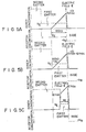
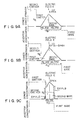
- FIG. 5A shows the case wherein the thickness W E of a first emitter layer is sufficiently large
- Figure 5B shows the case wherein the thickness W E of the first emitter layer is the same as a thickness W deP of the depletion layer caused by the internal potential difference
- Figure 5C is the case wherein the thickness W E of the first emitter layer is smaller than the thickness W de p.
- E max and E min are the maximum and minimum electric fields, respectively, in the first emitter layer.
- equation (7) can be derived so as to maximize the switching speed under constraint that W E does not exceed W de p at zero applied voltage as given by equation (3), and so as to set W e such that E max in equation (6) does not exceed the maximum allowable electric field of the heterojunction:
- V bi of the heterojunction between the first emitter layer and the base layer is given as follows: where k is Boltzmann's constant, T is absolute temperature, N B is the impurity concentration of the base layer, n i (T) is the intrinsic electron density of the base layer, XB is the electron affinity of the base layer, and Xe is the electron affinity of the first emitter layer.
- T absolute temperature
- N B is the impurity concentration of the base layer
- n i (T) is the intrinsic electron density of the base layer
- XB is the electron affinity of the base layer
- Xe is the electron affinity of the first emitter layer.
- the built-in potential V bi varies in accordance with various combinations of the impurities, as shown in Table 2.
- a bipolar transistor having a GaAIAs-GaAs structure is shown in Figure 6. The steps in manufacturing this bipolar transistor will be described.
- An n+ - type GaAs substrate 11 is used as the starting substrate.
- An n-type Si-doped GaAs collector layer 12 is formed by the epitaxial growth method on the GaAs substrate 11. With this process, a homojunction is to be formed between the collector and base layer. However, if a heterojunction is to be introduced for the collector-base junction, as n-type Ga 1-x Al x As layer may be formed on the GaAs substrate 11.
- MBE molecular beam epitaxy
- MOCVD metal-organic chemical vapor deposition
- a p-type Be-doped GaAs base layer 13 with relatively high impurity concentration is formed by the epitaxial growth method on the collector layer 12.
- a first emitter layer 14a of lightly doped n-type and a second emitter layer 14b of heavily doped n+ - type Ga 1-x Al x As are sequentially formed by the epitaxial growth method on the base layer 13.
- Si is used as the impurity, and the relationship between the concentration and the thickness of the first emitter layer 14a must satisfy equation (7).
- the resultant structure is selectively etched to leave only a central portion of the emitter, thereby exposing a peripheral portion of the surface of the base layer 13.
- Collector, base, and emitter electrodes 15, 16 and 17 are formed as shown to prepare the heterostructure bipolar transistor.
- the first emitter layer 14a consists of Ga 0.7 AI 0.3 As layer which has an energy gap of 1.80 eV, a donor concentration N E of 3x10 16 cm- 3 and a thickness W e of 0.1 ⁇ m.
- the base layer 13 consists of GaAs layer which has an energy gap of 1.42 eV and an acceptor concentration N B of 10 18 cm- 3 .
- the dielectric constant ⁇ SE of the first emitter layer is 12.0.
- W E 0.1 ⁇ m
- W E ⁇ W dep the maximum electric field E max is 1.75x10 5 V/cm from equation (6).
- V bl 1.55 V
- W deP 0.144 ⁇ m
- E (0) max 2.16X10 5 V/cm.
- W E ⁇ W dep , and E max 2 ⁇ 30x10 5 V/cm. Since the maximum allowable electric field E * max corresponding to the impurity concentration of 10 17 cm -3 is about 6.4x10 5 V/cm, the resultant device can be used in practice.
- An allowable applied voltage is about 4.0 V, so that a sufficient voltage-withstanding property is ensured.
- the switching characteristics of the two devices are slightly inferior to those of type B but are far superior to those of type A.
- the embodiment of the present invention can easily provide a practically sufficient voltage withstanding property.
- the emitter layer of a wide energy gap may consist of GaP, and the base layer of a narrow energy gap may consist of Si.
- the emitter layer consist of GaAs, and the base layer may consist of Ge.
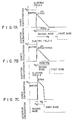
- FIG. 7A shows the case wherein the thickness W B of a second base layer of a low-impurity concentration is sufficiently large
- Figure 7B shows the case wherein W B of the second base layer is the same as a thickness W de p of a depletion layer caused by the internal potential difference
- Figure 7C is the case wherein W B is smaller than W de p.
- E max and E min are the maximum and minimum electric fields in the second base layer, respectively.
- equation (15) can be derived so as to maximize the switching speed under constraint that W does not exceed W de p at zero applied voltage as given by equation (11) and so as to set W B such that E max in equation (14) does not exceed the maximum allowable electric field of the heterojunction:
- V bi of the heterojunction between the second base layer and the emitter layer is given as follows: where k is Boltzmann's constant, T is absolute temperature, N E is the impurity concentration of the emitter layer, n,(T) is the intrinsic electron density of the second base layer, XB is the electron affinity of the second base layer, and XE is the electron affinity of the emitter layer.
- equation (16) the first term on the right-hand side is common to both the homojunction and the heterojunction, and the second term on the right-hand side is inherent to the heterojunction.
- the built-in potential V bl varies in accordance with various combinations of the impurities, as shown in Table 4.
- a bipolar transistor having a GaAIAs-GaAs structure is shown in Figure 8.
- the steps in manufacturing this bipolar transistor will be described.
- An n + -type GaAs substrate 21 is used as the starting substrate.
- An n-type Si-doped GaAs collector layer 22 is formed by the epitaxial growth method on the GaAs substrate 21. With this process, a homojunction is to be formed between the collector and base layers. However, if a heterojunction is to be introduced for the collector-base junction, an n-type Ga 1-x Al x As layer may be formed on the GaAs substrate 21.
- a p-type Be-doped GaAs first base layer 23a is formed by the epitaxial method on the collector layer 22.
- the first base layer 23a preferably has a thickness of 1,000 A or less in order to achieve high-speed switching.
- a p--type GaAs second base layer 23b and an n+ - type Ga 1-x Al x As emitter layer 24 are sequentially formed by the epitaxial growth method on the first base layer 23a. In this case, the relationship between the concentration and the thickness of the second base layer 23b must satisfy equation (15).
- the resultant structure is selectively etched to leave only a central portion of the emitter, thereby exposing a peripheral portion of the surface of the first base layer 23a.
- Collector, base, and emitter electrodes 25, 26, and 27 are deposited to prepare the heterostructure bipolar transistor.
- the emitter layer 24 consists of Ga 0.7 Al 0.3 As which has an energy gap of 1.80 eV and a donor concentration N E of 10 20 cm- 3 .
- the second base layer 23b consists of GaAs which has an energy gap of 1.42 eV, an acceptor concentration N B of 3x 10 16 cm- 3 , and a thickness W B of 0.1 ⁇ m.
- the dielectric constant ⁇ sB of the GaAs second base is 12.9.
- W B 0.1 ⁇ m
- a maximum electric field E * max allowable without generating junction breakdown at the impurity concentration N B of 3x10 16 cm -3 is about 5.1x10 5 V/cm. Since E max is lower than E * max , the above-mentioned design conditions which satisfy equation (15) are meaningful in practice.
- V bl 1.67 V
- W dep 0.154 ⁇ m
- An allowable applied voltage is about 4.0 V, thereby providing a sufficient voltage withstanding property as in the above devices.
- the switching characteristics of the two devices are slightly inferior to those of type B but are far superior to those of type A.
- the embodiment of the present invention can easily provide a practically acceptable voltage withstanding property.
- the emitter layer of a wide energy gap may consist of GaP, and the base layer of a narrow energy gap may consist of Si.
- the emitter layer may consist of GaAs, and the base layer may consist of Ge.
- Figure 9A shows the case wherein the thickness W E of the first emitter layer and the thickness W B of the second base layer are sufficiently large
- Figure 9B shows the case wherein the thicknesses W E and W B of the first emitter layer and the second base layer are equal to thicknesses W E,deP and W B , de p of depletion layers formed by the internal potential differences, respectively
- Figure 9C shows the case wherein the thicknesses W E and W B of the first emitter layer and the second base layer are smaller than thicknesses W E,dep and W B , de p of the depletion layers.
- equation (25) is derived so as to maximize the switching speed under constraint that N E W E 2 / ⁇ SE +N B W B 2 / ⁇ sg does not exceed the left hand side of equation (20), and that E max in equation (24) does not exceed the maximum allowable electric field of the heterojunction:
- V bl of the heterojunction between the second base layer and the first emitter layer is given as follows: where k is Boltzmann's constant, T is absolute temperature, N E is the impurity concentration of the emitter layer, n,(T) is the intrinsic electron density of the base layer, XB is the electron affinity of the second base layer, and X E is the electron affinity of the first emitter layer.
- equation (26) the first term in the right-hand side is common to both the homojunction and the heterojunction, and the second term on the right-hand side is inherent to the heterojunction.
- the built-in potential V bl varies in accordance with various combinations of the impurities, as shown in Table 6.
- a bipolar transistor having a GaAIAs-GaAs structure is shown in Figure 10.
- the steps in manufacturing this bipolar transistor will be described.
- An n+ - type GaAs substrate 31 is used as the starting substrate.
- An n-type Si-doped GaAs collector layer 32 is formed by the epitaxial growth method on the GaAs substrate 31. With this process, a homojunction is to be formed between the collector and base layers. However, if a heterojunction is to be introduced, an n-type Ga 1-x Al x As layer may be formed on the GaAs substrate 31. In both cases, molecular beam epitaxy or metal-organic chemical vapor deposition is preferably used for the epitaxial growth.
- a p-type Be-doped GaAs first base layer 33a and a p--type GaAs second base layer 33b are formed by the epitaxial growth method on the collector layer 32.
- a total thickness of the first and second base layers 33 is preferably 1,000 ⁇ or less so as to achieve high-speed switching.
- an n--type Ga 1-x Al x As first emitter layer 34a and an n + -type Ga 1-x Al x As second emitter layer 34b are formed by the epitaxial growth method on the base layers 33.
- Si is used as the impurity, and the relationship between the concentration and thickness of the first emitter layer 34a and that of the second base layer 33b are both set to satisfy equation (25). Finally, etching is performed to leave only a central portion of the emitter layer and expose the peripheral portion of the surface of the first base layer 33a. Collector, base, and emitter electrodes 35, 36, and 37 are formed to prepare the heterostructure bipolar transistor according to the third embodiment of the present invention.
- the second emitter layer 34b consists of Ga 0.7 Al 0.3 As which has an energy gap of 1.80 eV and a donor concentration N E0 of 10 2 ° cm- 3.
- the first emitter layer 34a consists of the same material as that of the second emitter layer 34b but has a donor concentration N E of 10 17 cm- 3 and a thickness W E of 500 A.
- the second base layer 33b consists of GaAs which has an acceptor concentration N B of 3x10 16 cm- 3 , a thickness W B of 500 A and an energy gap of 1.42 eV.
- the first base layer 33a consists of the same material as that of the second base layer 33b but has an acceptor concentration No of 10 18 cm- 3.
- the maximum electric field Emax becomes 1.70x10 5 V/cm in accordance with equation (24). Since the maximum allowable electric field E * max obtained without generating junction breakdown at the impurity concentration N E of 3x10 16 cm- 3 is about 5.1 x10 5 V/cm, E max is smaller than E * max . Therefore, the design conditions satisfy equation (25) and can be used in practice.
- V bl 1.49 V
- dep 1,050 A
- E (0) max 1.47X10 5 V/cm.
- the left-hand side of equation (25) is 4.02x10 5 (1/cm), and the right-hand side thereof is 1.65x10 6 (1/cm), thus satisfying equation (25).
- E max 2.49x10 5 V/cm is given, but E * max corresponding to the impurity concentration of 10 17 cm- 3 is about 6.4x 10 5 V/cm.
- the allowable applied voltage is about 4.5 V, thereby providing a sufficient voltage withstanding property.
- the switching characteristics of the two devices are slightly inferior to those of type B but are far superior to those of type A.
- the embodiment according to the present invention can easily provide a practically sufficient voltage withstanding property.
- the emitter layer of a wide energy gap may consist of GaP, and the base layer of a narrow energy gap may consist of Si.
- the emitter layer may consist of GaAs, and the base layer may consist of Ge.
Description
- The present invention relates to a heterostructure bipolar transistor using a heterojunction as an emitter-base junction.
- A conventional bipolar transistor has an npn or pnp structure wherein emitter, base, and collector layers are made of a common semiconductor material. in this case, emitter and collector junctions are each a homojunction.
- Bipolar transistors using a heterojunction as the emitter junction and/or collector junction are receiving a great deal of attention and are being extensively studied these days. The heterojunction bipolar transistor has an advantage in that, when the emitter layer is made of a semiconductor material having a wider energy gap than that of the base layer, the emitter injection efficiency can be enhanced. When the emitter junction is forward biased, carriers can be easily injected from the emitter to the base while carrier injection from the base to the emitter is limited due to an energy gap difference between the emitter and base layers. Therefore, the current gain of the heterostructure bipolar transistor becomes higher than that of the conventional homostructure type.
- The principle of the heterostructure bipolar transistors has been conventionally known. Recently, several examples have been published. Figure 1 shows the basic structure of conventional heterostructure bipolar transistors wherein a heterojunction is used as the emitter junction. This transistor comprises a GaAs-GaAIAs structure. An n-type
GaAs collector layer 2, a p-typeGaAs base layer 3, and an n-type Ga1-xAlxAs emitter layer 4 are sequentially deposited on an n+-type GaAs substrate 1.Reference numeral 5 denotes a collector electrode; 6, a base electrode; and 7, an emitter electrode. The emitter layer 4 comprises an n--type first emitter layer 4a which is in contact with thebase layer 3, and an n+-type second emitter layer 4b which is in contact with the emitter electrode 7. A common feature of conventional heterostructure bipolar transistors is in that the first emitter layer 4a is thick. The structure in which the emitter layer comprises a two-layer structure of high- and low-impurity concentration layers and the first emitter layer is thick aims at decreasing the emitter junction capacitance so that the switching speed is increased (e.g., H. Kroemer "Heterostructure Bipolar Transistors and Integrated Circuits", Proc. IEEE, Vol. 70, No. 1, PP. 13-25, January 1982). In fact, when the low-impurity concentration layer has a sufficient thickness in a one-sided abrupt junction constituted by such high- and low-impurity concentration layers, it is known that the junction capacitance CJE can be expressed, in terms of an impurity concentration NE of the low-impurity concentration layer, as follows:
- In order to clarify the subsequent discussion, the concept of the switching speed of a transistor will be clarified. In general, the switching operation of transistors includes turn-on and turn-off. The propagation delay time tpd, the average value of a turn-on time ton and a turn-off time toff, is taken as a reference of the switching speed. When an input signal of Figure 2 is supplied to a transistor, the turn-on time ton is defined to be a time for an output current to increase from 0% to 50%, and the turn-off time toff is defined to be a time for the output current to decrease from 100% to 50% (see Figure 3).
- The present inventors have made extensive studies of thicknesses of the respective layers and the relationship between the impurity concentration and the switching speed of the heterostructure bipolar transistor shown in Figure 1, by means of a numerical analysis model (e.g., M. Kurata "Principles of Operation of Bipolar Transistors", 1980, Kindai Kagaku-sha, and M. Kurata, "Numerical Analysis for Semiconductor Devices", 1982, Lexington Books, D. C. Heath and Company). The present inventors have reached an opposite conclusion to the conventional theory. In particular, they found that the switching speed of the conventional transistor (to be referred to as type A hereafter) having the first emitter layer of a low-impurity concentration and a large thickness was greatly lower than that of a transistor (to be referred to as type B hereinafter) having only a single high-impurity concentration layer (omitting the first emitter layer). The results are shown in Table 1.

- In this numerical analysis, conditions are given in the circuit shown in Figure 4 such that a collector power supply voltage Ec=2 V, a load resistance RL=200 0, and an output signal voltage to turn transistor Q off Voff=0.5 V. An input signal voltage to turn transistor Q on Von is given in Table 1. In type A, the first emitter layer has an impurity concentration NE of 3x1016 cm-3 and a thickness W of 1 µm. Je and Jc denote current densities of the emitter and the collector, respectively.
- The opposite conclusion described above is based on the following reasoning. In general, in order to switch the bipolar transistor at a high speed, the emitter and collector current densities must be set from 103 to 104 A/cm2 or higher. This fact is apparent from various experiments and from analytical results using the numerical analysis model. With the transistor of type A having the first emitter layer of a low-impurity concentration, the capability to inject carriers from the emitter to the base is smaller than that of type B. In order to obtain predetermined emitter and collector current densities, a high forward-bias voltage must be applied across the emitter-base junction. Under this operating condition, excess carriers are stored in the thick first emitter layer and the collector layer. As a result, the turn-off time is increased, and hence the propagation delay time is increased.
- In fine, the emitter junction capacitance CJE of type A is smaller than that of type B, but the switching speed of type A is lower than that of type B. This result implies that both the emitter junction capacitance CJE and a total emitter capacitance CE=CJE+CDE must be considered as factors in determining the switching speed of the transistor, where CDE is known as the emitter diffusion capacitance, which is determined by the excess carrier charge. Since the thick first emitter layer of a low-impurity concentration is formed in the conventional heterostructure bipolar transistor, CDE is greater than CJE. An effect of a small CJE cannot be observed under the influence of CDE with respect to the switching speed.
- It is apparent that type B is preferred to type A from the point of view of switching speed. However, since type B has the emitter layer of a high-impurity concentration directly formed on the base layer, the breakdown voltage of the emitter junction is very low. The breakdown of a p-n junction mainly occurs due to the avalanche phenomenon. Even if the avalanche phenomenon is prevented, however, breakdown can also occur due to the tunneling effect. In particular, in the heterostructure bipolar transistor, the current caused by the tunneling effect consists of a component controlled by a number of interface levels generated at the heterojunction interface, in addition to a component determined by the direct transition of carriers between energy bands. For this reason, in practice, the tunneling current often becomes greater than a theoretical value. As a result, the emitter-junction breakdown voltage becomes very low.
- In "A Depletion Stop Double Base Phototransistor: A Demonstration of a New Transistor Structure" by C. Y. Chen et al., IEDM 81, PP. 267-270, are disclosed a double base structure for phototransistors which is composed of a lightly doped layer near the emitter junction and a heavily doped layer near the collector junction, and a double-emitter double-base structure which is composed of lightly doped base and emitter layers near the emitter junction, heavily doped base and emitter layers far from the emitter junction. However, no specific formula to define the layer concentration and thickness is given. In addition, in the prior art device, the problem caused by excess carrier charge is left unsolved. It is noted that the phototransistor differs from the bipolar transistor of the present invention.
- It is an object of the present invention to provide an improved heterostructure bipolar transistor with high switching speed.
- It is another object of the present invention to provide an improved heterostructure bipolar transistor having a high breakdown voltage.
- In order to achieve the above objects of the present invention, there is provided a heterostructure bipolar transistor comprising an emitter layer, a base layer and a collector layer. The emitter layer is formed of a semiconductor material whose energy gap is wider than that of said base layer, so that a heterojunction is formed between the emitter layer and the base layer. One of said emitter layer and said base layer comprises first and second layers which are sequentially formed, the first layer constituting the heterojunction has a lower impurity concentration than that of the second layer, and when the impurity concentration and the thickness of the first layer are defined as N, and W1, respectively, the following relation is satisfied:

- q: the absolute value of electron charge (=1.6x10⁻¹⁹ Coulombs)
- so: the free space permittivity (=8.86x10⁻¹⁴ farads/cm)
- εs1: the dielectric constant of the first layer, and
- Vbi: the built-in potential at the heterojunction.
- In addition, the other of the aforementioned emitter layer or the base layer comprises third and fourth layers which are sequentially formed, and third layer constituting the heterojunction has a lower impurity concentration than that of the fourth layer. When the impurity concentration and the thickness of the third layer are defined as N2 and W2, respectively, the following relation is satisfied:

- q: the absolute value of electron charge (=1.6x10⁻¹⁹ Coulombs)
- so: the free space permittivity (=8.86x10⁻¹⁴ farads/cm)
- εS1: the dielectric constant of the first layer
- εs2: the dielectric constant of the third layer
- Vbl: the built-in potential at the heterojunction.
- According to the arrangement described above, a heterostructure bipolar transistor which is improved in the switching speed and voltage withstanding property can be obtained. In addition, various problems caused by excess carrier storage can be solved.
- Other objects and advantages will be apparent from the following description taken in conjunction with the accompanying drawings, in which:
- Figure 1 is a sectional view of a conventional heterostructure bipolar transistor;
- Figures 2 and 3 are respectively timing charts for clarifying the concept of the switching speed of a transistor;
- Figure 4 is a diagram of a circuit used for numerically analyzing the switching speed of a transistor;
- Figures 5A to 5C are respectively graphs showing the impurity concentration distribution and the electric field distribution of base and emitter layers so as to explain the theoretical background of a first embodiment of the present invention;
- Figure 6 is a sectional view of a heterostructure bipolar transistor according to the first embodiment of the present invention;
- Figures 7A to 7C are respectively graphs showing the impurity concentration distribution and the electric field distribution of base and emitter layers so as to explain the theoretical background of a second embodiment of the present invention;
- Figure 8 is a sectional view of a heterostructure bipolar transistor according to the second embodiment of the present invention;
- Figures 9A to 9C are respectively graphs showing the impurity concentration distribution and the electric field distribution of base and emitter layers so as to explain the theoretical background of a third embodiment of the present invention; and
- Figure 10 is a sectional view of a heterostructure bipolar transistor according to the third embodiment of the present invention.
- The theoretical background of a first embodiment will be described with reference to Figures 5A to 5C. When a voltage of zero volts is applied across an emitter-base heterojunction, an internal potential difference across this junction is a built-in potential Vbl· The electric field distribution of the heterojunction caused by the built-in potential Vbi becomes as shown in Figures 5A to 5C. Figure 5A shows the case wherein the thickness WE of a first emitter layer is sufficiently large, Figure 5B shows the case wherein the thickness WE of the first emitter layer is the same as a thickness WdeP of the depletion layer caused by the internal potential difference, and Figure 5C is the case wherein the thickness WE of the first emitter layer is smaller than the thickness Wdep. When the impurity concentration NE of the first emitter layer is much lower than the impurity concentration NB of the base layer, the cases shown in Figures 5A and 5B respectively are known to satisfy the following equations:


- Elimination of

- Similarly, the case shown in Figure 5C satisfies the following equations:


- Deriving Emax from these equations:

- Under the assumptions described above, equation (7) can be derived so as to maximize the switching speed under constraint that WE does not exceed Wdep at zero applied voltage as given by equation (3), and so as to set We such that Emax in equation (6) does not exceed the maximum allowable electric field of the heterojunction:

- The built-in potential Vbi of the heterojunction between the first emitter layer and the base layer is given as follows:

- When the first emitter layer consists of n-type Ga0.7Al0.3As and the base layer consists of p-type GaAs, the built-in potential Vbi varies in accordance with various combinations of the impurities, as shown in Table 2.

- A first embodiment of the present invention will now be described. A bipolar transistor having a GaAIAs-GaAs structure is shown in Figure 6. The steps in manufacturing this bipolar transistor will be described. An n+-type GaAs substrate 11 is used as the starting substrate. An n-type Si-doped
GaAs collector layer 12 is formed by the epitaxial growth method on the GaAs substrate 11. With this process, a homojunction is to be formed between the collector and base layer. However, if a heterojunction is to be introduced for the collector-base junction, as n-type Ga1-xAlxAs layer may be formed on the GaAs substrate 11. In both cases, molecular beam epitaxy (MBE) or metal-organic chemical vapor deposition (MOCVD) is preferably used for the epitaxial growth. In the subsequent processes, either method may be applied. Thereafter, a p-type Be-dopedGaAs base layer 13 with relatively high impurity concentration is formed by the epitaxial growth method on thecollector layer 12. Thebase layer 13 preferably has a thickness of 1,000 Å(10 Å=1 nm) or less in order to achieve high-speed switching operation. A first emitter layer 14a of lightly doped n-type and asecond emitter layer 14b of heavily doped n+-type Ga1-xAlxAs are sequentially formed by the epitaxial growth method on thebase layer 13. In this case, Si is used as the impurity, and the relationship between the concentration and the thickness of the first emitter layer 14a must satisfy equation (7). The resultant structure is selectively etched to leave only a central portion of the emitter, thereby exposing a peripheral portion of the surface of thebase layer 13. Collector, base, andemitter electrodes - More specifically, the first emitter layer 14a consists of Ga0.7AI0.3As layer which has an energy gap of 1.80 eV, a donor concentration NE of 3x1016 cm-3 and a thickness We of 0.1 µm. On the other hand, the
base layer 13 consists of GaAs layer which has an energy gap of 1.42 eV and an acceptor concentration NB of 1018 cm-3. In this case, the built-in potential Vbl at a temperature of T=300°K becomes 1.52 V when XE=3.77 eV; XB=4.07 eV and nI(T)=1.101x107 cm-3 are substituted in equation (8). - When a zero voltage is applied between the emitter and base layers, the thickness Wdep and the maximum electric field E(0) max of the depletion layer to be extended when the first emitter layer 14a is sufficiently thick are obtained from equations (1) and (2) such that Wdep=0.260 µm and E(0) max=1.17X10⁵ V/cm. In this case, the dielectric constant εSE of the first emitter layer is 12.0. However, since WE=0.1 µm, WE< Wdep. In this case, the maximum electric field Emax is 1.75x10⁵ V/cm from equation (6). A maximum electric field E*max allowable without generating junction breakdown at the impurity concentration NE of 3x1016 cm-3 is about 5.1x10⁵ V/cm (S. M. Sze, "Physics of Semiconductor Devices", 1969, Wiley-Interscience). Since the above Emax is lower than E* max, the above-mentioned design conditions which satisfy equation (7) are meaningful in practice. In fact, an applied voltage such that Emax=E* max is about 3.3 V, ensuring a sufficient voltage-withstanding property.
- Another device may be prepared using the same materials described above but under different conditions, namely: NE=1017 cm-3, WE=0.1 um, and NB=1018 cm-3. In this case, Vbl=1.55 V, WdeP=0.144 µm, and E(0) max=2.16X10⁵ V/cm. At this time, WE<Wdep, and Emax=2·30x105 V/cm. Since the maximum allowable electric field E* max corresponding to the impurity concentration of 1017 cm-3 is about 6.4x10⁵ V/cm, the resultant device can be used in practice. An allowable applied voltage is about 4.0 V, so that a sufficient voltage-withstanding property is ensured.
- The switching characteristics of the two devices described above, which are obtained by numerical analysis, are shown in Table 3. The circuit conditions are the same as those in Table 1.
- Comparing these results with those in Table 1, the switching characteristics of the two devices are slightly inferior to those of type B but are far superior to those of type A. Unlike type B wherein the emitter-base voltage withstanding property is poor, the embodiment of the present invention can easily provide a practically sufficient voltage withstanding property.
- In this embodiment, the emitter layer of a wide energy gap may consist of GaP, and the base layer of a narrow energy gap may consist of Si. Alternatively, the emitter layer consist of GaAs, and the base layer may consist of Ge.

- The theoretical background of a second embodiment of the present invention will be described with reference to Figures 7A to 7C. When a voltage of zero volts is applied to a heterojunction between the emitter and the base, the internal potential difference across this junction is Vbl. The electric field distribution of the heterojunction, casued by Vbi, is shown as in Figures 7A to 7C. Figure 7A shows the case wherein the thickness WB of a second base layer of a low-impurity concentration is sufficiently large, Figure 7B shows the case wherein WB of the second base layer is the same as a thickness Wdep of a depletion layer caused by the internal potential difference, and Figure 7C is the case wherein WB is smaller than Wdep. When the impurity concentration NE of the first emitter layer is much higher than the impurity concentration NB of the base layer, the cases shown in Figures 7A and 7B respectively satisfy the following equations:


- Elimination of


- Similarly, the case shown in Figure 7C satisfies the following equations:


- Deriving Emax from these equations:

- Under the assumptions described above, equation (15) can be derived so as to maximize the switching speed under constraint that W does not exceed Wdep at zero applied voltage as given by equation (11) and so as to set WB such that Emax in equation (14) does not exceed the maximum allowable electric field of the heterojunction:

- The built-in potential Vbi of the heterojunction between the second base layer and the emitter layer is given as follows:

- When the emitter layer consists of n-type Ga0.7Al0.3As and the second base layer consists of p-type GaAs, the built-in potential Vbl varies in accordance with various combinations of the impurities, as shown in Table 4.

- The second embodiment of the present invention will now be described. A bipolar transistor having a GaAIAs-GaAs structure is shown in Figure 8. The steps in manufacturing this bipolar transistor will be described. An n+-
type GaAs substrate 21 is used as the starting substrate. An n-type Si-dopedGaAs collector layer 22 is formed by the epitaxial growth method on theGaAs substrate 21. With this process, a homojunction is to be formed between the collector and base layers. However, if a heterojunction is to be introduced for the collector-base junction, an n-type Ga1-xAlxAs layer may be formed on theGaAs substrate 21. In both cases, molecular beam epitaxy or metal-organic chemical vapor deposition is preferably used for the epitaxial growth. In the subsequent processes, either method may be applied. Thereafter, a p-type Be-doped GaAsfirst base layer 23a is formed by the epitaxial method on thecollector layer 22. Thefirst base layer 23a preferably has a thickness of 1,000 A or less in order to achieve high-speed switching. A p--type GaAssecond base layer 23b and an n+-type Ga1-xAlxAsemitter layer 24 are sequentially formed by the epitaxial growth method on thefirst base layer 23a. In this case, the relationship between the concentration and the thickness of thesecond base layer 23b must satisfy equation (15). The resultant structure is selectively etched to leave only a central portion of the emitter, thereby exposing a peripheral portion of the surface of thefirst base layer 23a. Collector, base, andemitter electrodes - In particular, the
emitter layer 24 consists of Ga0.7Al0.3As which has an energy gap of 1.80 eV and a donor concentration NE of 1020 cm-3. On the other hand, thesecond base layer 23b consists of GaAs which has an energy gap of 1.42 eV, an acceptor concentration NB of 3x 1016 cm-3, and a thickness WB of 0.1 µm. In this case, the built-in potenial Vbl at a temperature of T=300°K is 1.64 V when XE=3.77 eV, XB=4.07 eV, and ni(T)=1.101x107 cm-3 are substituted in equation (16). - When a voltage of zero volts is applied between the emitter and base layers, the thickness Wdep and the maximum electric field E(0) max of the depletion layer to be extended when the
second base layer 23b is sufficiently thick are obtained from equations (9) and (10) such that Wdep=0.279 µm and E(0) max=1.17x10⁵ V/cm. In this case, the dielectric constant εsB of the GaAs second base is 12.9. However, since WB=0.1 µm, WB<WdeP. In this case, the maximum electric field Emax is Emax=1.85x10⁵ V/cm from equation (14). A maximum electric field E* max allowable without generating junction breakdown at the impurity concentration NB of 3x1016 cm-3 is about 5.1x10⁵ V/cm. Since Emax is lower than E* max, the above-mentioned design conditions which satisfy equation (15) are meaningful in practice. An applied voltage such that Emax=E* max is 3.2 V. - Another device may be prepared using the same materials described above but under different conditions, namely: NE=1020 cm-3, NB=1017 cm-3 and WB=0.1 µm. In this case, Vbl=1.67 V, Wdep=0.154 µm, and E(0) max=2.16X10⁵ V/cm are obtained. Therefore, WB<Wdep and Emax=2.37x10⁵ V/cm. Since the maximum allowable electric field E*max corresponding to the impurity concentration of 1017 cm-3 is about 6.4x10⁵ V/cm, the resultant device can be used in practice. An allowable applied voltage is about 4.0 V, thereby providing a sufficient voltage withstanding property as in the above devices.
- The switching characteristics of the two devices described above, which are obtained by numerical analysis, are shown in Table 5. The circuit conditions are the same as those in Table 1.

- Comparing these results with those in Table 1, the switching characteristics of the two devices are slightly inferior to those of type B but are far superior to those of type A. Unlike type B wherein the emitter-base voltage withstanding property is poor, the embodiment of the present invention can easily provide a practically acceptable voltage withstanding property.
- In this embodiment, the emitter layer of a wide energy gap may consist of GaP, and the base layer of a narrow energy gap may consist of Si. Alternatively, the emitter layer may consist of GaAs, and the base layer may consist of Ge.
- The theoretical background of a third embodiment of the present invention will now be described with reference to Figures 9A to 9C.
- When a voltage of zero volts is applied across the heterojunction between the emitter and the base, the internal potential difference appearing across the junction is Vbl. The electric field distribution of the heterojunction caused by the potential difference becomes as shown in Figures 9A to 9C. Figure 9A shows the case wherein the thickness WE of the first emitter layer and the thickness WB of the second base layer are sufficiently large, Figure 9B shows the case wherein the thicknesses WE and WB of the first emitter layer and the second base layer are equal to thicknesses WE,deP and WB,dep of depletion layers formed by the internal potential differences, respectively, and Figure 9C shows the case wherein the thicknesses WE and WB of the first emitter layer and the second base layer are smaller than thicknesses WE,dep and WB,dep of the depletion layers. In the cases shown in Figures 9A and 9B, equations (17), (18), and (19) are obtained in accordance with a known theory:


- Elimination of Emax from equations (17) and (18) yields:

- Similarly, the case shown in Figure 9C satisfies equations (21), (22) and (23):


- Obtaining Emax from equations (21), (22), and (23),

- It should be noted that the maximum electric yield in the depletion layers, the minimum electric field in the first emitter layer, and the minimum electric field in the second base layer are given as Emax, Emin.E and Emin,B respectively.
- Under the assumption described above, equation (25) is derived so as to maximize the switching speed under constraint that NEWE 2/εSE+NBWB 2/εsg does not exceed the left hand side of equation (20), and that Emax in equation (24) does not exceed the maximum allowable electric field of the heterojunction:

- The built-in potential Vbl of the heterojunction between the second base layer and the first emitter layer is given as follows:

- When the first emitter layer consists of n-type Ga0.7Al0.3As and the second base layer consists of p-type GaAs, the built-in potential Vbl varies in accordance with various combinations of the impurities, as shown in Table 6.

- The third embodiment of the present invention will now be described. A bipolar transistor having a GaAIAs-GaAs structure is shown in Figure 10. The steps in manufacturing this bipolar transistor will be described. An n+-
type GaAs substrate 31 is used as the starting substrate. An n-type Si-dopedGaAs collector layer 32 is formed by the epitaxial growth method on theGaAs substrate 31. With this process, a homojunction is to be formed between the collector and base layers. However, if a heterojunction is to be introduced, an n-type Ga1-xAlxAs layer may be formed on theGaAs substrate 31. In both cases, molecular beam epitaxy or metal-organic chemical vapor deposition is preferably used for the epitaxial growth. In the subsequent processes, either method may be applied. Thereafter, a p-type Be-doped GaAs first base layer 33a and a p--type GaAs second base layer 33b are formed by the epitaxial growth method on thecollector layer 32. A total thickness of the first and second base layers 33 is preferably 1,000 Å or less so as to achieve high-speed switching. Subsequently, an n--type Ga1-xAlxAs first emitter layer 34a and an n+-type Ga1-xAlxAssecond emitter layer 34b are formed by the epitaxial growth method on the base layers 33. In this case, Si is used as the impurity, and the relationship between the concentration and thickness of the first emitter layer 34a and that of the second base layer 33b are both set to satisfy equation (25). Finally, etching is performed to leave only a central portion of the emitter layer and expose the peripheral portion of the surface of the first base layer 33a. Collector, base, andemitter electrodes - In particular, the
second emitter layer 34b consists of Ga0.7Al0.3As which has an energy gap of 1.80 eV and a donor concentration NE0 of 102° cm-3. The first emitter layer 34a consists of the same material as that of thesecond emitter layer 34b but has a donor concentration NE of 1017 cm-3 and a thickness WE of 500 A. On the other hand, the second base layer 33b consists of GaAs which has an acceptor concentration NB of 3x1016 cm-3, a thickness WB of 500 A and an energy gap of 1.42 eV. The first base layer 33a consists of the same material as that of the second base layer 33b but has an acceptor concentration No of 1018 cm-3. In this case, the built-in potential VbI at a temperature T of 300°K is 1.46 V when XE=3.77 eV, XB=4.07 eV and ni(T)=1.101x107 cm-3 are substituted in equation (26). - The thicknesses WE,dep and WB,deP of the depletion layers, in the case when the first emitter layer and the second base layer are sufficiently thick, and the maximum electric field E(0) max are WE,deP=651 A, We,deP=2,332 A and E(0) max=0.98X10⁵ V/cm from equations (17), (18) and (19), respectively. It should be noted that dielectric constants εSE and εse of the emitter and base layers are 12.0 and 12.9, respectively. However, since WE=WB=500 A, the left-hand side of equation (25) is calculated to be 2.66x10⁵ (1/cm) and the right-hand side thereof is calculated to be 1.62x 10⁶ (1/cm), so that equation (25) is satisfied. In this case, the maximum electric field Emax becomes 1.70x10⁵ V/cm in accordance with equation (24). Since the maximum allowable electric field E* max obtained without generating junction breakdown at the impurity concentration NE of 3x1016 cm-3 is about 5.1 x10⁵ V/cm, Emax is smaller than E* max. Therefore, the design conditions satisfy equation (25) and can be used in practice. As a reference, an applied voltage for Emax=E* max is about 3.3 V.
- Another device may be formed using the same materials as described above, but under different manufacturing conditions, namely: NE0=1020 cm-3, NE=1017 cm-3, NB0=1018 cm-3, NB=1017 cm-3 and WE=WB=500 A. In this case, Vbl=1.49 V, WE,dep=977 A and WB,dep=1,050 A, and E(0) max=1.47X10⁵ V/cm. At the same time, the left-hand side of equation (25) is 4.02x10⁵ (1/cm), and the right-hand side thereof is 1.65x10⁶ (1/cm), thus satisfying equation (25). In addition, Emax=2.49x10⁵ V/cm is given, but E* max corresponding to the impurity concentration of 1017 cm-3 is about 6.4x 10⁵ V/cm. Thus, these design conditions can also be used in practice. The allowable applied voltage is about 4.5 V, thereby providing a sufficient voltage withstanding property.
- The switching characteristics of the two devices described above, which are obtained by numerical analysis, are shown in Table 7. The circuit conditions are the same as those in Table 1.

- Comparing these results with those in Table 1, the switching characteristics of the two devices are slightly inferior to those of type B but are far superior to those of type A. Unlike type B wherein the emitter-base voltage withstanding property is poor, the embodiment according to the present invention can easily provide a practically sufficient voltage withstanding property.
- In this embodiment, the emitter layer of a wide energy gap may consist of GaP, and the base layer of a narrow energy gap may consist of Si. Alternatively, the emitter layer may consist of GaAs, and the base layer may consist of Ge.
Claims (4)
Applications Claiming Priority (6)
| Application Number | Priority Date | Filing Date | Title |
|---|---|---|---|
| JP8606983A JPS59211266A (en) | 1983-05-17 | 1983-05-17 | Hetero junction bipolar transistor |
| JP86069/83 | 1983-05-17 | ||
| JP86072/83 | 1983-05-17 | ||
| JP8607283A JPS59211268A (en) | 1983-05-17 | 1983-05-17 | Hetero junction bipolar transistor |
| JP8606383A JPS59211265A (en) | 1983-05-17 | 1983-05-17 | Hetero junction bipolar transistor |
| JP86063/83 | 1983-05-17 |
Publications (3)
| Publication Number | Publication Date |
|---|---|
| EP0132025A2 EP0132025A2 (en) | 1985-01-23 |
| EP0132025A3 EP0132025A3 (en) | 1987-01-07 |
| EP0132025B1 true EP0132025B1 (en) | 1989-08-09 |
Family
ID=27305067
Family Applications (1)
| Application Number | Title | Priority Date | Filing Date |
|---|---|---|---|
| EP84303235A Expired EP0132025B1 (en) | 1983-05-17 | 1984-05-11 | Heterostructure bipolar transistor |
Country Status (3)
| Country | Link |
|---|---|
| US (1) | US4593305A (en) |
| EP (1) | EP0132025B1 (en) |
| DE (1) | DE3479368D1 (en) |
Families Citing this family (32)
| Publication number | Priority date | Publication date | Assignee | Title |
|---|---|---|---|---|
| JPH0626242B2 (en) * | 1983-12-05 | 1994-04-06 | 富士通株式会社 | Semiconductor integrated circuit device |
| NL8501769A (en) * | 1984-10-02 | 1986-05-01 | Imec Interuniversitair Micro E | BIPOLAR HIGH-JUNCTION TRANSISTOR AND METHOD FOR THE MANUFACTURE THEREOF. |
| US5060234A (en) * | 1984-11-19 | 1991-10-22 | Max-Planck Gesellschaft Zur Forderung Der Wissenschaften | Injection laser with at least one pair of monoatomic layers of doping atoms |
| JPS61198776A (en) * | 1985-02-28 | 1986-09-03 | Fujitsu Ltd | Hetero-junction bipolar transistor and manufacture thereof |
| JPS61248561A (en) * | 1985-04-25 | 1986-11-05 | インタ−ナショナル・ビジネス・マシ−ンズ・コ−ポレ−ション | Semiconductor structural body |
| DE3679947D1 (en) * | 1985-08-26 | 1991-08-01 | Toshiba Kawasaki Kk | SEMICONDUCTOR ARRANGEMENTS AND METHOD FOR THE PRODUCTION BY MEANS OF ION IMPLANTATION. |
| US4716445A (en) * | 1986-01-17 | 1987-12-29 | Nec Corporation | Heterojunction bipolar transistor having a base region of germanium |
| DE3788527T2 (en) * | 1986-04-01 | 1994-05-11 | Matsushita Electric Ind Co Ltd | Bipolar transistor and its manufacturing process. |
| EP0257460B1 (en) * | 1986-08-12 | 1996-04-24 | Canon Kabushiki Kaisha | Solid-state electron beam generator |
| US4738624A (en) * | 1987-04-13 | 1988-04-19 | International Business Machines Corporation | Bipolar transistor structure with self-aligned device and isolation and fabrication process therefor |
| US4872040A (en) * | 1987-04-23 | 1989-10-03 | International Business Machines Corporation | Self-aligned heterojunction transistor |
| JP2533541B2 (en) * | 1987-06-08 | 1996-09-11 | 株式会社日立製作所 | Heterojunction bipolar transistor |
| JP2542676B2 (en) * | 1987-07-02 | 1996-10-09 | 株式会社東芝 | Heterojunction bipolar transistor |
| JP2619407B2 (en) * | 1987-08-24 | 1997-06-11 | 株式会社日立製作所 | Method for manufacturing semiconductor device |
| US4839303A (en) * | 1987-10-13 | 1989-06-13 | Northrop Corporation | Planar bipolar transistors including heterojunction transistors and method |
| US4821082A (en) * | 1987-10-30 | 1989-04-11 | International Business Machines Corporation | Heterojunction bipolar transistor with substantially aligned energy levels |
| US4825269A (en) * | 1988-03-04 | 1989-04-25 | Stanford University | Double heterojunction inversion base transistor |
| EP0355464A3 (en) * | 1988-08-15 | 1990-04-18 | Motorola, Inc. | Heterojunction bipolar transistor formed on a critically misoriented substrate |
| US5064772A (en) * | 1988-08-31 | 1991-11-12 | International Business Machines Corporation | Bipolar transistor integrated circuit technology |
| US4967253A (en) * | 1988-08-31 | 1990-10-30 | International Business Machines Corporation | Bipolar transistor integrated circuit technology |
| US4981807A (en) * | 1988-10-31 | 1991-01-01 | International Business Machines Corporation | Process for fabricating complementary vertical transistor memory cell |
| US4956689A (en) * | 1989-04-12 | 1990-09-11 | Texas Instruments Incorporated | High speed gallium arsenide transistor and method |
| EP0445475B1 (en) * | 1990-02-20 | 1998-08-26 | Kabushiki Kaisha Toshiba | Heterojunction bipolar transistor |
| DE69128123T2 (en) * | 1990-08-31 | 1998-03-05 | Texas Instruments Inc | Process for the production of self-aligning bipolar transistors with heterojunction |
| US5132764A (en) * | 1991-03-21 | 1992-07-21 | Texas Instruments Incorporated | Multilayer base heterojunction bipolar transistor |
| US5208184A (en) * | 1991-04-30 | 1993-05-04 | Texas Instruments Incorporated | P-n junction diffusion barrier employing mixed dopants |
| US5448087A (en) * | 1992-04-30 | 1995-09-05 | Trw Inc. | Heterojunction bipolar transistor with graded base doping |
| US5365089A (en) * | 1992-12-23 | 1994-11-15 | International Business Machines Corporation | Double heterojunction bipolar transistor and the method of manufacture therefor |
| US6107151A (en) * | 1997-05-09 | 2000-08-22 | Research Triangle Institute | Heterojunction bipolar transistor and method of manufacturing |
| TW512529B (en) | 2000-06-14 | 2002-12-01 | Infineon Technologies Ag | Silicon bipolar transistor, circuit arrangement and method for producing a silicon bipolar transistor |
| JP3730483B2 (en) | 2000-06-30 | 2006-01-05 | 株式会社東芝 | Bipolar transistor |
| US9425260B2 (en) | 2014-03-13 | 2016-08-23 | International Business Machines Corporation | Application of super lattice films on insulator to lateral bipolar transistors |
Family Cites Families (3)
| Publication number | Priority date | Publication date | Assignee | Title |
|---|---|---|---|---|
| JPS5638064B2 (en) * | 1974-04-02 | 1981-09-03 | ||
| CA1136773A (en) * | 1978-08-14 | 1982-11-30 | Norikazu Ohuchi | Semiconductor device |
| US4380774A (en) * | 1980-12-19 | 1983-04-19 | The United States Of America As Represented By The Secretary Of The Navy | High-performance bipolar microwave transistor |
-
1984
- 1984-05-08 US US06/608,217 patent/US4593305A/en not_active Expired - Lifetime
- 1984-05-11 DE DE8484303235T patent/DE3479368D1/en not_active Expired
- 1984-05-11 EP EP84303235A patent/EP0132025B1/en not_active Expired
Also Published As
| Publication number | Publication date |
|---|---|
| EP0132025A2 (en) | 1985-01-23 |
| EP0132025A3 (en) | 1987-01-07 |
| DE3479368D1 (en) | 1989-09-14 |
| US4593305A (en) | 1986-06-03 |
Similar Documents
| Publication | Publication Date | Title |
|---|---|---|
| EP0132025B1 (en) | Heterostructure bipolar transistor | |
| US4901132A (en) | Semiconductor integrated circuit with switching bipolar transistors having high withstand voltage capability | |
| EP0033876B1 (en) | Three-terminal semiconductor device | |
| KR20030063075A (en) | Heterojunction bipolar transistor and semiconductor integrated circuit device using the same | |
| US4782379A (en) | Semiconductor device having rapid removal of majority carriers from an active base region thereof at device turn-off and method of fabricating this device | |
| EP0228107B1 (en) | Fast switching lateral insulated gate transistors | |
| EP0615292A1 (en) | Insulated gate bipolar transistor | |
| US4712122A (en) | Heterojunction gate ballistic JFET with channel thinner than Debye length | |
| EP0080044B1 (en) | Semiconductor device having rapid removal of majority carriers from an active base region thereof at device turn-off and method of fabricating this device | |
| EP0014080B1 (en) | A three-terminal semiconductor switch device | |
| US4649411A (en) | Gallium arsenide bipolar ECL circuit structure | |
| CA1299771C (en) | Heterojunction bipolar transistor with collector buffer layer | |
| JPH0560263B2 (en) | ||
| EP0208294B1 (en) | Three-dimensional integrated circuit | |
| US4027180A (en) | Integrated circuit transistor arrangement having a low charge storage period | |
| EP0249088B1 (en) | A semiconductor device | |
| US5461245A (en) | Article comprising a bipolar transistor with floating base | |
| EP0361759B1 (en) | Heterostructure bipolar transistor | |
| US4616242A (en) | Enhancement and depletion mode selection layer for field effect transistor | |
| CA1211563A (en) | Integrated circuit arrangement | |
| US4121116A (en) | Component for logic circuits and logic circuits equipped with this component | |
| JPH0618210B2 (en) | Heterojunction bipolar transistor | |
| JP2587826B2 (en) | Bipolar transistor and method of manufacturing the same | |
| US4656498A (en) | Oxide-isolated integrated Schottky logic | |
| Ishida et al. | Orientation effect on AlGaAs/GaAs heterojunction bipolar transistors |
Legal Events
| Date | Code | Title | Description |
|---|---|---|---|
| PUAI | Public reference made under article 153(3) epc to a published international application that has entered the european phase |
Free format text: ORIGINAL CODE: 0009012 |
|
| 17P | Request for examination filed |
Effective date: 19840601 |
|
| AK | Designated contracting states |
Designated state(s): DE FR GB NL |
|
| PUAL | Search report despatched |
Free format text: ORIGINAL CODE: 0009013 |
|
| AK | Designated contracting states |
Kind code of ref document: A3 Designated state(s): DE FR GB NL |
|
| 17Q | First examination report despatched |
Effective date: 19880812 |
|
| 18W | Application withdrawn |
Withdrawal date: 19890303 |
|
| D18W | Application withdrawn (deleted) | ||
| GRAA | (expected) grant |
Free format text: ORIGINAL CODE: 0009210 |
|
| AK | Designated contracting states |
Kind code of ref document: B1 Designated state(s): DE FR GB |
|
| REF | Corresponds to: |
Ref document number: 3479368 Country of ref document: DE Date of ref document: 19890914 |
|
| ET | Fr: translation filed | ||
| PLBE | No opposition filed within time limit |
Free format text: ORIGINAL CODE: 0009261 |
|
| STAA | Information on the status of an ep patent application or granted ep patent |
Free format text: STATUS: NO OPPOSITION FILED WITHIN TIME LIMIT |
|
| 26N | No opposition filed | ||
| PGFP | Annual fee paid to national office [announced via postgrant information from national office to epo] |
Ref country code: GB Payment date: 19970502 Year of fee payment: 14 |
|
| PGFP | Annual fee paid to national office [announced via postgrant information from national office to epo] |
Ref country code: FR Payment date: 19970513 Year of fee payment: 14 |
|
| PGFP | Annual fee paid to national office [announced via postgrant information from national office to epo] |
Ref country code: DE Payment date: 19970516 Year of fee payment: 14 |
|
| PG25 | Lapsed in a contracting state [announced via postgrant information from national office to epo] |
Ref country code: GB Free format text: LAPSE BECAUSE OF NON-PAYMENT OF DUE FEES Effective date: 19980511 |
|
| PG25 | Lapsed in a contracting state [announced via postgrant information from national office to epo] |
Ref country code: FR Free format text: LAPSE BECAUSE OF NON-PAYMENT OF DUE FEES Effective date: 19980531 |
|
| GBPC | Gb: european patent ceased through non-payment of renewal fee |
Effective date: 19980511 |
|
| PG25 | Lapsed in a contracting state [announced via postgrant information from national office to epo] |
Ref country code: DE Free format text: LAPSE BECAUSE OF NON-PAYMENT OF DUE FEES Effective date: 19990302 |
|
| REG | Reference to a national code |
Ref country code: FR Ref legal event code: ST |