EP0131809B1 - Dicing apparatus - Google Patents
Dicing apparatus Download PDFInfo
- Publication number
- EP0131809B1 EP0131809B1 EP84107440A EP84107440A EP0131809B1 EP 0131809 B1 EP0131809 B1 EP 0131809B1 EP 84107440 A EP84107440 A EP 84107440A EP 84107440 A EP84107440 A EP 84107440A EP 0131809 B1 EP0131809 B1 EP 0131809B1
- Authority
- EP
- European Patent Office
- Prior art keywords
- flange
- wafer
- dicing
- cooling water
- dicing blade
- Prior art date
- Legal status (The legal status is an assumption and is not a legal conclusion. Google has not performed a legal analysis and makes no representation as to the accuracy of the status listed.)
- Expired
Links
Images


Classifications
-
- B—PERFORMING OPERATIONS; TRANSPORTING
- B28—WORKING CEMENT, CLAY, OR STONE
- B28D—WORKING STONE OR STONE-LIKE MATERIALS
- B28D5/00—Fine working of gems, jewels, crystals, e.g. of semiconductor material; apparatus or devices therefor
-
- B—PERFORMING OPERATIONS; TRANSPORTING
- B23—MACHINE TOOLS; METAL-WORKING NOT OTHERWISE PROVIDED FOR
- B23D—PLANING; SLOTTING; SHEARING; BROACHING; SAWING; FILING; SCRAPING; LIKE OPERATIONS FOR WORKING METAL BY REMOVING MATERIAL, NOT OTHERWISE PROVIDED FOR
- B23D59/00—Accessories specially designed for sawing machines or sawing devices
- B23D59/02—Devices for lubricating or cooling circular saw blades
-
- B—PERFORMING OPERATIONS; TRANSPORTING
- B23—MACHINE TOOLS; METAL-WORKING NOT OTHERWISE PROVIDED FOR
- B23D—PLANING; SLOTTING; SHEARING; BROACHING; SAWING; FILING; SCRAPING; LIKE OPERATIONS FOR WORKING METAL BY REMOVING MATERIAL, NOT OTHERWISE PROVIDED FOR
- B23D61/00—Tools for sawing machines or sawing devices; Clamping devices for these tools
- B23D61/02—Circular saw blades
- B23D61/10—Circular saw blades clamped between hubs; Clamping or aligning devices therefor
-
- B—PERFORMING OPERATIONS; TRANSPORTING
- B28—WORKING CEMENT, CLAY, OR STONE
- B28D—WORKING STONE OR STONE-LIKE MATERIALS
- B28D5/00—Fine working of gems, jewels, crystals, e.g. of semiconductor material; apparatus or devices therefor
- B28D5/02—Fine working of gems, jewels, crystals, e.g. of semiconductor material; apparatus or devices therefor by rotary tools, e.g. drills
- B28D5/022—Fine working of gems, jewels, crystals, e.g. of semiconductor material; apparatus or devices therefor by rotary tools, e.g. drills by cutting with discs or wheels
- B28D5/023—Fine working of gems, jewels, crystals, e.g. of semiconductor material; apparatus or devices therefor by rotary tools, e.g. drills by cutting with discs or wheels with a cutting blade mounted on a carriage
Definitions
- This invention relates to a dicing apparatus which is for the microelectronic circuit fabrication such as semi-conductor integrated circuit or large scale integrated circuit fabrication separating a wafer into individual small-dimensioned die.
- the dicing apparatus there are three types of the dicing apparatus; a diamond scribing, a laser scribing, and a diamond wheel sawing type.
- this invention relates to the diamond wheel sawing type which cuts the wafer by a rotating diamond dicing blade.
- the dicing blade has a very sharp circle edge like 10-30 Ilm thickness and rotates at very high speed like 20,000-30,000 revolutions per minute. Therefore, the dicing blade is formed in a very thin disk having a hole at the center and is fitted to a rotating spindle being caught between two flanges.
- the dicing apparatus has a cooling system which pours coolant against a cutting interface.
- Water is usually used as a coolant spurting from a coolant nozzle so as to: firstly lower the temperature at the cutting interface; secondly provide lubrication between the cutting edge and the wafer; and finally clean cutting debris away from the cutting area.
- the present invention especially relates to cleaning the cutting debris improving the water pouring mechanism of the cooling system, because it has been a great deal of trouble that the cutting debris causes cutting objects such as the wafers and dice to damage in the prior art.
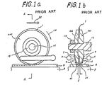
- Figs. 1a and 1b show the illustrating diagrams of the dicing apparatus of the prior art using a dicing blade; Fig. 1 a shows the front view and Fig. 1b shows the sectional view at A-A in Fig. 1a.
- reference numeral 1 is a dicing blade which is caught by flanges 201 and 202 from both sides of the dicing blade, fitted to a spindle 12, and fixed by a nut 14, each 3 is a coolant nozzle with a coolant pipe from which cooling water 7 spurts and flows along a direction 8 because of the rotation of flanges 201 and 202 and blade 1, 4 is a wafer to be cut, 5 is a dicing street along which the wafer 4 is cut and separated to dice, 61 and 62 are bonding pads on each of which a lead wire is bonded in the process of die assembling, 9 is a stage on which the wafer is mounted to be cut, an arrow 20 indicates a rotating direction of the dicing blade 1, and an arrow 21 indicates a running direction of the rotating spindle 12.
- Fig. 1 a shows that the dicing apparatus is working under the down-cut mode, if the direction of 20 or 21 was reversed, the cutting mode would be changed to a up-cut mode.
- these two cutting modes are used to save the time of the cutting process by running the dicing blade back-and-forth on the wafer.
- the dicing blade works under the down-cut mode, plenty of cutting debris hit the surface of the wafer with the cooling water splashed by the rotating flanges causing the bonding pads on the wafer such as 61 and 62 to damage.
- the surface of the wafer 4 is coated by the coating material such as a Silicon Dioxide or Phospho-Silicate Glass to protect the fabricated microelectronic circuit on the wafer from the damage and dirt.
- the coating material can not be applied on the bonding pads and the dicing streets, because the bonding pads are for bonding the lead wires and the dicing streets are for cutting the wafer.
- the bonding pads are very dilicate, because they are made of the metal like aluminum, so the cutting debris easily sticks into them. If so, poor bonding or- increase of connected resistance will occur after bonding; this has been really a big problem because this has often deteriorated the quality and reliability of a fabricated semiconductor die.
- the problem in the prior art will be explained more in Figs. 2a and 2b.
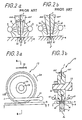
- Fig. 2a is a diagram around the cutting interface using the dicing apparatus of the prior art.
- Fig. 2b is also a diagram of the same cutting interface especially showing the flow of the cooling water being poured against the cutting interface.
- reference numerals having the same numerals to Figs. 1 a and 1 indicate the same objects.
- the flanges 201 and 202 are made so that each flange becomes thin to decrease the weight of the flanges to maintain the high speed rotation of the dicing blade. So, the width (t,) at the circumference of the flange edge is so thin as 200-300 pm, and an angle (8 1 ) between the tapered side-surface of the flange 201 or 202 and the side-surface of the dicing blade is so narrow as 10-12 degrees.
- each bonding pad is usually located so that the distance from the center of the dicing street 5 to the center of the bonding pad is approximately 100 pm. Consequently, as shown in Fig.
- the cooling water 7 spurting out from the coolant nozzle 3 is splashed at the tapered side-surface of the flange 201 or 202 and flows along the tapered side-surface of the flange by the centrifugal force of the flange rotation.
- the water flow 7 shows this. Therefore, the cooling water violently hits the bonding pads 61 or 62 and behaves like a hammer, so that the water sticks the cutting debris, which are on the bonding pad, into the bonding pad, and in other case, the water carries the cutting debris and sticks them into the bonding pad 61 or 62. This has been a big trouble to fabricate the microelectronic dice by the dicing apparatus using the dicing blade of the prior art.
- the purpose of the present invention is to avoid the cutting debris sticking into the bonding pad on account of the cooling water accelerated by the side-surfaces of the rotating flanges which catch the dicing blade, when the dicing apparatus applying the rotating dicing blade to cut the microelectronic wafer under the down-cut mode.
- This purpose is achieved by the features of the specific clause of claim 1.
- the surface of the bonding pad can be kept clean, so that the wrong bonding connection by the cutting debris can be avoided.
- the quality and the reliability of a fabricated semiconductor die and the yield of the semiconductor device production have been conspicuously improved.
- Fig. 3 shows an illustrating diagram of an embodiment of the invented dicing apparatus
- Fig. 4 depicts several embodiments of improved flanges and the flows of cooling water
- Fig. 5 depicts several embodiments of coolant nozzles.
- Figs. 3a and 3b are similar figures to Figs. 1a and 1b except for the flanges and the coolant nozzles.
- Fig. 3a is a front view of the dicing apparatus
- Fig. 3b is a sectional view at B-B in Fig. 3a.
- reference numeral 131 and 132 show the embodiments of flanges
- 15 shows the embodiment of a coolant nozzle
- dotted lines 16 show the cooling water pouring against the cutting interface from the nozzle
- 17 shows a dicing wheel which is a rotating body comprising the flanges 131 and 132 and the dicing blade 1 being put between the flanges.
- Fig. 3a shows the dicing apparatus of the present invention which is sawing the semiconductor wafer.
- the rotating direction 20 and running direction 21 show that the dicing apparatus works under the down-cut mode.
- the present invention is applied to the flanges 131 and 132 and the coolant nozzle 15. As seen in Fig.
- the side-surfaces of the flanges 131 and 132 are in parallel with the side-faces of the dicing blade 1, in other words, the side-surfaces of the flanges 131 and 132 and the upper surface of the wafer 4 meet at right angles, and the thickness (t 2 ) of the flange edge part of the dicing wheel 17 is larger than the distance between the outer sides of bonding pads 61 and 62 putting the cutting street 5 between them; for example, t 2 is 1 mm when the distance between the outer sides of bonding pads 61 and 62 is 200-400 pm.
- the extending surface of the side-surface of the flange 131, 132 crosses the wafer 4 at the position apart from the bonding pads 61, 62 in some distance.
- the cooling water splashed by the rotating dicing wheel 17 at the high speed can be poured on the surface of the wafer 4 avoiding the direct collision of the cooling water on the bonding pads 61 and 62.
- the thickness of the dicing wheel 17 near by the spindle 12 is set larger than t 2 as shown in Fig. 3b, this thickness is mainly to keep the strength of the flanges 131 and 132, but there is another effect to improve the cooling water flow. This will be disclosed in the following explanation of Fig. 4a.
- Fig. 3a and 3b show the flange extracted from Figs. 3a and 3b
- Figs. 4b and 4c show other embodiments of the flanges.
- reference numeral 23, 231 or 232 is respectively an edge-face at the circumference of the flanges 131 and 132
- an arrow of reference numeral 22, 221 or 222 shows respectively an improved flow of the cooling water.
- Fig. 4a the improved flow of the cooling water is explained more.
- the cooling water flow there are two kinds of the cooling water flow in this case; one is an outer flow 221 and the other is an inner flow 222, each flow works for cooling and lubricating the cutting interface, and cleaning the debris away from the cutting area, however a major flow is the outer flow 221 and the innerflow 222 is a minor flow.
- the distance between the flow 222 at both sides of the dicing wheel 17 is larger than the distance between the outer sides of the bonding pads 61 and 62 looking from the dicing street 5.
- the dicing wheel 17 is so thick as 3-4 mm to maintain the strength of the flanges 131 and 132 and the thickness is given as far as approximately the edge of the flange circumference, the side surface of the flanges 131 and 132 are in parallel with the surface of the dicing blade 1, and each edge-surface (reference numeral 23) at the circumference of flange 131 or 132 makes an angle 8 so as to be more than 60 degrees to the surface of the dicing blade 1.
- the cooling water poured onto both sides of the dicing wheel 17 from the nozzles is accelerated by the centrifugal force of the rotating dicing wheel 17 and is splashed along the flow 221 hitting violently respective portions of the surface of the wafer 4, however each portion is in sufficient distance from the bonding pad 61 or 62.
- the minor cooling water flows along the flow 222 and is poured on the cutting interface, however, as the force of the minor cooling water is weak and it is not directed to the bonding pads 61, 62 directly, the bonding pads 61 and 62 are not damaged by the cutting debris. Consequently, the damage of the bonding pads 61 and 62 by the cutting debris can be avoided.
- the flanges 131 and 132 are tapered so as to decrease the weight of the dicing wheel 17.
- the cooling water at the both side of the dicing wheel 17 are accelerated by the centrifugal force of the rotating dicing wheel 17 and each of the cooling water is poured on a portion of the surface of the wafer 4. Therefore, in this case, the tapered angle must be taken so that the portion is in sufficient distance from the bonding pad 61 or 62.
- the coolant nozzle is also the point of the present invention.
- the direction of each cooling water 16 spurted from respective coolant nozzle 15 is improved so that the cooling water from nozzle 15 is poured more aslant than that of the prior art to the surface of the cutting interface, furthermore, as the thickness of the flange of the present invention becomes thick, the coolant nozzle 15 must be brought closer to the surface of the wafer 4 comparing with the prior art.
- the nozzle 15 is a horizontal slit so that the cooling water is concentrated on to the cutting interface of the dicing blade. As a result, the cooling water can be supplied sufficiently to the cutting interface, so the cutting speed can be increased without reducing the cutting quality.
- Figs. 5a, 5b; 6a, 6b; 7a, 7b show the diagrams to illustrate the embodiments of the invented nozzles.
- reference numeral 31 is a cooling water supply pipe
- 32 is a slit for the cooling water spurting
- 33 is an upper guard to prevent the cooling water spurting upward from the slit 32 and guide it downward to let it pour the cutting interface
- 34 is a nozzle guide to guide the cooling water spurting from the slit 32 to the designated cutting interface.
- the slit which runs in parallel with the axis of the coolant pipe; in parallel with the surface of the wafer, such as the slit 32 shown in Fig. 5a, 6a, or 7a can be applied to the coolant pipe of the prior art having a plurality of the slits provided perpendicularly to the axis of the coolant pipe or to the surface of the wafer.
- Fig. 8a and 8b Fig. 8a is a front view of the embodiment and Fig. 8b shows a sectional view at C-C in Fig. 8a of the embodiment.
- 31 is a coolant pipe
- 322 are vertical slits of the prior art
- 321 is a horizontal slit.
- even the coolant pipe of the prior art can be improved to pour the cooling water properly and effectively to the cutting interface by providing the horizontal slit 321 to the coolant pipe 31.
Landscapes
- Engineering & Computer Science (AREA)
- Mechanical Engineering (AREA)
- Dicing (AREA)
- Processing Of Stones Or Stones Resemblance Materials (AREA)
Description
- This invention relates to a dicing apparatus which is for the microelectronic circuit fabrication such as semi-conductor integrated circuit or large scale integrated circuit fabrication separating a wafer into individual small-dimensioned die.
- Generally, there are three types of the dicing apparatus; a diamond scribing, a laser scribing, and a diamond wheel sawing type. Above all, this invention relates to the diamond wheel sawing type which cuts the wafer by a rotating diamond dicing blade. To fabricate precisely, the dicing blade has a very sharp circle edge like 10-30 Ilm thickness and rotates at very high speed like 20,000-30,000 revolutions per minute. Therefore, the dicing blade is formed in a very thin disk having a hole at the center and is fitted to a rotating spindle being caught between two flanges.
- Furthermore, the dicing apparatus has a cooling system which pours coolant against a cutting interface. Water is usually used as a coolant spurting from a coolant nozzle so as to: firstly lower the temperature at the cutting interface; secondly provide lubrication between the cutting edge and the wafer; and finally clean cutting debris away from the cutting area. The present invention especially relates to cleaning the cutting debris improving the water pouring mechanism of the cooling system, because it has been a great deal of trouble that the cutting debris causes cutting objects such as the wafers and dice to damage in the prior art.
- Figs. 1a and 1b show the illustrating diagrams of the dicing apparatus of the prior art using a dicing blade; Fig. 1 a shows the front view and Fig. 1b shows the sectional view at A-A in Fig. 1a. In the figures, reference numeral 1 is a dicing blade which is caught by
flanges spindle 12, and fixed by anut 14, each 3 is a coolant nozzle with a coolant pipe from which cooling water 7 spurts and flows along a direction 8 because of the rotation offlanges blade 1, 4 is a wafer to be cut, 5 is a dicing street along which thewafer 4 is cut and separated to dice, 61 and 62 are bonding pads on each of which a lead wire is bonded in the process of die assembling, 9 is a stage on which the wafer is mounted to be cut, anarrow 20 indicates a rotating direction of the dicing blade 1, and anarrow 21 indicates a running direction of the rotatingspindle 12. - There are two cutting modes when the dicing blade saws the wafer: one is a up-cut mode and the other is a down-cut mode. Fig. 1 a shows that the dicing apparatus is working under the down-cut mode, if the direction of 20 or 21 was reversed, the cutting mode would be changed to a up-cut mode. Usually these two cutting modes are used to save the time of the cutting process by running the dicing blade back-and-forth on the wafer. However, when the dicing blade works under the down-cut mode, plenty of cutting debris hit the surface of the wafer with the cooling water splashed by the rotating flanges causing the bonding pads on the wafer such as 61 and 62 to damage.
- The surface of the
wafer 4 is coated by the coating material such as a Silicon Dioxide or Phospho-Silicate Glass to protect the fabricated microelectronic circuit on the wafer from the damage and dirt. However, the coating material can not be applied on the bonding pads and the dicing streets, because the bonding pads are for bonding the lead wires and the dicing streets are for cutting the wafer. - Above all, the bonding pads are very dilicate, because they are made of the metal like aluminum, so the cutting debris easily sticks into them. If so, poor bonding or- increase of connected resistance will occur after bonding; this has been really a big problem because this has often deteriorated the quality and reliability of a fabricated semiconductor die. The problem in the prior art will be explained more in Figs. 2a and 2b.
- Fig. 2a is a diagram around the cutting interface using the dicing apparatus of the prior art. Fig. 2b is also a diagram of the same cutting interface especially showing the flow of the cooling water being poured against the cutting interface. In the figures, reference numerals having the same numerals to Figs. 1 a and 1 indicate the same objects.
- As shown in Fig. 2a, in the dicing apparatus of the prior art, the
flanges flange dicing street 5 to the center of the bonding pad is approximately 100 pm. Consequently, as shown in Fig. 2b, the cooling water 7 spurting out from thecoolant nozzle 3 is splashed at the tapered side-surface of theflange bonding pads bonding pad - The purpose of the present invention is to avoid the cutting debris sticking into the bonding pad on account of the cooling water accelerated by the side-surfaces of the rotating flanges which catch the dicing blade, when the dicing apparatus applying the rotating dicing blade to cut the microelectronic wafer under the down-cut mode. This purpose is achieved by the features of the specific clause of claim 1. As the effect of the present invention, the surface of the bonding pad can be kept clean, so that the wrong bonding connection by the cutting debris can be avoided. As a result, the quality and the reliability of a fabricated semiconductor die and the yield of the semiconductor device production have been conspicuously improved.
-
- Fig. 1 a is a schematic front view of the prior art dicing apparatus.
- Fig. 1 b is a schematic sectional view at A-A in Fig. 1a of the prior art dicing apparatus.
- Fig. 2a is a fragmentary sectional view of the flanges, the dicing blade, and the coolant nozzles of the prior art with the cutting interface.
- Fig. 2b is a equal fragmentary sectional view to Fig. 2a showing the cooling water flowing along the rotating flanges and dicing blade.
- Fig. 3a is a schematic front view of the embodiment of the present invention dicing apparatus.
- Fig. 3b is a schematic sectional view at B-B in Fig. 3a of the embodiment of the present invention dicing apparatus.
- Fig. 4a is a fragmentary sectional view of the flanges of the present invention and the dicing blade with the cutting interface showing the cooling water flows along the rotating flanges and dicing blade.
- Fig. 4b is a fragmentary sectional view of another flange of the present invention and the dicing blade with the cutting interface showing the cooling water flowing along the rotating flanges and dicing blade.
- Fig. 4c is a fragmentary sectional view of still another flange of the present invention and the dicing blade with the cutting interface showing the cooling water flows along the rotating flanges and dicing blade.
- Fig. 5a is a schematic front view of the coolant nozzle of the present invention.
- Fig. 5b is a schematic sectional view of the coolant nozzle of the present invention of Fig. 5a.
- Fig. 6a is a schematic front view of another coolant nozzle of the present invention.
- Fig. 6b is a schematic sectional view of the coolant nozzle of the present invention of Fig. 6a.
- Fig. 7a is a schematic front view of still another coolant nozzle of the present invention.
- Fig. 7b is a schematic sectional view of the coolant nozzle of the present invention of Fig. 7a.
- Fig. 8a is a schematic front view of a further coolant nozzle of the present invention.
- Fig. 8b is a schematic sectional view of the coolant nozzle of the present invention of Fig. 8a.
- The preferred embodiment of the present invention will be disclosed showing Figs. 3, 4 and 5. Fig. 3 shows an illustrating diagram of an embodiment of the invented dicing apparatus, Fig. 4 depicts several embodiments of improved flanges and the flows of cooling water, and Fig. 5 depicts several embodiments of coolant nozzles.
- Figs. 3a and 3b are similar figures to Figs. 1a and 1b except for the flanges and the coolant nozzles. Fig. 3a is a front view of the dicing apparatus, and Fig. 3b is a sectional view at B-B in Fig. 3a. In the figures, reference numerals having the same numerals to Figs. 1a and 1b correspond individually the same objects to them,
reference numeral nozzle flanges - Fig. 3a shows the dicing apparatus of the present invention which is sawing the semiconductor wafer. The
rotating direction 20 and runningdirection 21 show that the dicing apparatus works under the down-cut mode. In the figure, the present invention is applied to theflanges coolant nozzle 15. As seen in Fig. 3b, the side-surfaces of theflanges flanges wafer 4 meet at right angles, and the thickness (t2) of the flange edge part of thedicing wheel 17 is larger than the distance between the outer sides ofbonding pads street 5 between them; for example, t2 is 1 mm when the distance between the outer sides ofbonding pads flange wafer 4 at the position apart from thebonding pads rotating dicing wheel 17 at the high speed can be poured on the surface of thewafer 4 avoiding the direct collision of the cooling water on thebonding pads dicing wheel 17 near by thespindle 12 is set larger than t2 as shown in Fig. 3b, this thickness is mainly to keep the strength of theflanges - The
flange reference numeral flanges reference numeral - In Fig. 4a, the improved flow of the cooling water is explained more. There are two kinds of the cooling water flow in this case; one is an
outer flow 221 and the other is aninner flow 222, each flow works for cooling and lubricating the cutting interface, and cleaning the debris away from the cutting area, however a major flow is theouter flow 221 and theinnerflow 222 is a minor flow. As mentioned before, the distance between theflow 222 at both sides of thedicing wheel 17 is larger than the distance between the outer sides of thebonding pads street 5. Furthermore, major cooling water of theflow 221 at both sides of thedicing wheel 17 are poured on the respective portions of the surface of thewafer 4, each portion is in sufficient distance from thebonding pad flow 222 being poured around thebonding pads flow 222 is so weak that the debris on thebonding pads bonding pads - In the embodiment of Fig. 4b, the
dicing wheel 17 is so thick as 3-4 mm to maintain the strength of theflanges flanges flange dicing wheel 17 from the nozzles is accelerated by the centrifugal force of therotating dicing wheel 17 and is splashed along theflow 221 hitting violently respective portions of the surface of thewafer 4, however each portion is in sufficient distance from thebonding pad flow 222 and is poured on the cutting interface, however, as the force of the minor cooling water is weak and it is not directed to thebonding pads bonding pads bonding pads - In the embodiment of Fig. 4c, the
flanges dicing wheel 17. In this structure, the cooling water at the both side of thedicing wheel 17 are accelerated by the centrifugal force of therotating dicing wheel 17 and each of the cooling water is poured on a portion of the surface of thewafer 4. Therefore, in this case, the tapered angle must be taken so that the portion is in sufficient distance from thebonding pad - As mentioned before, the coolant nozzle is also the point of the present invention. As shown in Figs. 3a and 3b of the present invention, the direction of each cooling water 16 spurted from
respective coolant nozzle 15 is improved so that the cooling water fromnozzle 15 is poured more aslant than that of the prior art to the surface of the cutting interface, furthermore, as the thickness of the flange of the present invention becomes thick, thecoolant nozzle 15 must be brought closer to the surface of thewafer 4 comparing with the prior art. Another point is that, since the quantity of the cooling water pouring to the cutting interface of the dicing blade caused by the centrifugal force is small in the present invention, thenozzle 15 is a horizontal slit so that the cooling water is concentrated on to the cutting interface of the dicing blade. As a result, the cooling water can be supplied sufficiently to the cutting interface, so the cutting speed can be increased without reducing the cutting quality. - Figs. 5a, 5b; 6a, 6b; 7a, 7b show the diagrams to illustrate the embodiments of the invented nozzles. In the figures, each figure having mark "a" shows the side view and having mark "b" shows the cutting view,
reference numeral 31 is a cooling water supply pipe, 32 is a slit for the cooling water spurting, 33 is an upper guard to prevent the cooling water spurting upward from theslit 32 and guide it downward to let it pour the cutting interface, 34 is a nozzle guide to guide the cooling water spurting from theslit 32 to the designated cutting interface. - The slit which runs in parallel with the axis of the coolant pipe; in parallel with the surface of the wafer, such as the
slit 32 shown in Fig. 5a, 6a, or 7a can be applied to the coolant pipe of the prior art having a plurality of the slits provided perpendicularly to the axis of the coolant pipe or to the surface of the wafer. This is shown in Fig. 8a and 8b; Fig. 8a is a front view of the embodiment and Fig. 8b shows a sectional view at C-C in Fig. 8a of the embodiment. In this figure, 31 is a coolant pipe, 322 are vertical slits of the prior art, and 321 is a horizontal slit. As shown in this figure, even the coolant pipe of the prior art can be improved to pour the cooling water properly and effectively to the cutting interface by providing thehorizontal slit 321 to thecoolant pipe 31. - Applying the present invention to the dicing apparatus in such a. way as mentioned above, the cutting debris on the bonding pads can be protected from sticking into the pads by the poured pressure of the cooling water, so that wrong bonding connections by the cutting debris can be avoided. As a result, the quality and the reliability of a fabricated semiconductor die and the yield of the semiconductor device production have been conspicuously improved. For example, the fraction defective assuming because of the cutting debris sticking into the bonding pads was as much as 2-3% in the prior art, however applying the present invention, this has been improved to as little as 0.2-0.3%.
Claims (8)
characterised in that the plane of each outer side-surface of the flanges (131, 132) crosses the surface of said wafer in sufficient outward distance from said bonding pad looking from said cutting street.
Applications Claiming Priority (2)
| Application Number | Priority Date | Filing Date | Title |
|---|---|---|---|
| JP124517/83 | 1983-07-08 | ||
| JP58124517A JPS6030314A (en) | 1983-07-08 | 1983-07-08 | Dicing device |
Publications (2)
| Publication Number | Publication Date |
|---|---|
| EP0131809A1 EP0131809A1 (en) | 1985-01-23 |
| EP0131809B1 true EP0131809B1 (en) | 1988-09-07 |
Family
ID=14887432
Family Applications (1)
| Application Number | Title | Priority Date | Filing Date |
|---|---|---|---|
| EP84107440A Expired EP0131809B1 (en) | 1983-07-08 | 1984-06-28 | Dicing apparatus |
Country Status (5)
| Country | Link |
|---|---|
| US (1) | US4569326A (en) |
| EP (1) | EP0131809B1 (en) |
| JP (1) | JPS6030314A (en) |
| KR (1) | KR900001993B1 (en) |
| DE (1) | DE3473985D1 (en) |
Cited By (1)
| Publication number | Priority date | Publication date | Assignee | Title |
|---|---|---|---|---|
| DE9015096U1 (en) * | 1990-11-02 | 1991-04-18 | Lindner, Horst, 8400 Regensburg | Saw for cutting material samples |
Families Citing this family (20)
| Publication number | Priority date | Publication date | Assignee | Title |
|---|---|---|---|---|
| DE8901638U1 (en) * | 1989-01-31 | 1989-06-22 | Frost, Günther, 8400 Regensburg | Device for separating a plate-shaped panel having several printed circuits |
| US5252079A (en) * | 1992-02-10 | 1993-10-12 | Amp Incorporated | Method of manufacture of a contact guide |
| US5261385A (en) * | 1992-03-27 | 1993-11-16 | Dicing Technology Inc. | Abrasive cutting blade assembly with multiple cutting edge exposures |
| US5613350A (en) * | 1992-12-24 | 1997-03-25 | Boucher; John N. | Method for packaging and handling fragile dicing blade |
| JP3209818B2 (en) * | 1993-03-08 | 2001-09-17 | 株式会社東京精密 | Cutting blade mounting structure for dicing equipment |
| EP0676253A1 (en) * | 1994-04-06 | 1995-10-11 | Motorola, Inc. | A chamfered hub blade |
| US6152803A (en) * | 1995-10-20 | 2000-11-28 | Boucher; John N. | Substrate dicing method |
| US5718615A (en) * | 1995-10-20 | 1998-02-17 | Boucher; John N. | Semiconductor wafer dicing method |
| JPH08205633A (en) * | 1995-10-27 | 1996-08-13 | Yanmar Agricult Equip Co Ltd | Ambulatory transplanter |
| KR100225909B1 (en) * | 1997-05-29 | 1999-10-15 | 윤종용 | Wafer sawing apparatus |
| JP3497071B2 (en) * | 1997-11-20 | 2004-02-16 | 東芝機械株式会社 | Contour processing method and processing machine |
| JP3482331B2 (en) * | 1997-12-17 | 2003-12-22 | 東芝機械株式会社 | Finishing method |
| US20040112360A1 (en) * | 1998-02-12 | 2004-06-17 | Boucher John N. | Substrate dicing method |
| RU2155131C2 (en) * | 1998-09-11 | 2000-08-27 | Ульяновский государственный технический университет | Method of cutting silicon single crystals |
| JP3485816B2 (en) * | 1998-12-09 | 2004-01-13 | 太陽誘電株式会社 | Dicing equipment |
| US20030136394A1 (en) * | 2002-01-18 | 2003-07-24 | Texas Instruments Incorporated | Dicing saw having an annularly supported dicing blade |
| JP4753170B2 (en) * | 2004-03-05 | 2011-08-24 | 三洋電機株式会社 | Semiconductor device and manufacturing method thereof |
| JP2013069814A (en) * | 2011-09-21 | 2013-04-18 | Renesas Electronics Corp | Method for manufacturing semiconductor device |
| JP5955530B2 (en) * | 2011-11-02 | 2016-07-20 | 株式会社ディスコ | Cutting equipment |
| JP2024050022A (en) * | 2022-09-29 | 2024-04-10 | 株式会社ディスコ | Cutting device and cutting method |
Family Cites Families (8)
| Publication number | Priority date | Publication date | Assignee | Title |
|---|---|---|---|---|
| US2163687A (en) * | 1938-01-10 | 1939-06-27 | Bucyrus Monighan Company | Cutting |
| CH223824A (en) * | 1940-10-19 | 1942-10-15 | Lindner Herbert | Outlet nozzle on grinding machines for supplying the grinding fluid to the grinding wheel. |
| GB865811A (en) * | 1958-01-23 | 1961-04-19 | James Thomas Pascoe | Improvements in or relating to circular saw assemblies |
| US3886925A (en) * | 1973-06-20 | 1975-06-03 | Barrie F Regan | Cutting wheel |
| FR2382097A1 (en) * | 1977-02-23 | 1978-09-22 | Radiotechnique Compelec | PROCESS FOR MANUFACTURING SEMICONDUCTOR DIODES OF TYPE P-I-N |
| JPS56126937A (en) * | 1980-03-11 | 1981-10-05 | Toshiba Corp | Cutting apparatus for semiconductor wafer |
| JPS57203553U (en) * | 1981-06-23 | 1982-12-24 | ||
| JPS58111346A (en) * | 1981-12-25 | 1983-07-02 | Hitachi Ltd | dicing equipment |
-
1983
- 1983-07-08 JP JP58124517A patent/JPS6030314A/en active Granted
-
1984
- 1984-06-28 EP EP84107440A patent/EP0131809B1/en not_active Expired
- 1984-06-28 DE DE8484107440T patent/DE3473985D1/en not_active Expired
- 1984-06-28 KR KR1019840003696A patent/KR900001993B1/en not_active Expired
- 1984-07-09 US US06/628,862 patent/US4569326A/en not_active Expired - Fee Related
Cited By (1)
| Publication number | Priority date | Publication date | Assignee | Title |
|---|---|---|---|---|
| DE9015096U1 (en) * | 1990-11-02 | 1991-04-18 | Lindner, Horst, 8400 Regensburg | Saw for cutting material samples |
Also Published As
| Publication number | Publication date |
|---|---|
| US4569326A (en) | 1986-02-11 |
| KR900001993B1 (en) | 1990-03-31 |
| JPH0145978B2 (en) | 1989-10-05 |
| KR850001062A (en) | 1985-03-14 |
| DE3473985D1 (en) | 1988-10-13 |
| JPS6030314A (en) | 1985-02-15 |
| EP0131809A1 (en) | 1985-01-23 |
Similar Documents
| Publication | Publication Date | Title |
|---|---|---|
| EP0131809A1 (en) | Dicing apparatus | |
| US6105567A (en) | Wafer sawing apparatus having washing solution spray and suction devices for debris removal and heat dissipation | |
| US6737606B2 (en) | Wafer dicing device and method | |
| US7064014B2 (en) | Backside metallization on sides of microelectronic dice for effective thermal contact with heat dissipation devices | |
| US8449356B1 (en) | High pressure cooling nozzle for semiconductor package | |
| US6291317B1 (en) | Method for dicing of micro devices | |
| EP1502695A1 (en) | Finishing machine using laser beam | |
| US7057136B2 (en) | Finishing machine using laser beam | |
| US20190389091A1 (en) | Semiconductor Sawing Method and System | |
| JP2019102514A (en) | Cutting method | |
| CN215750090U (en) | Cutting machine with inclined water spraying opening | |
| JP4786949B2 (en) | Cutting equipment | |
| JPH04245663A (en) | Semiconductor wafer dicing method and dicing blade cooling mechanism | |
| JP2005057160A (en) | Dicing device | |
| JP2829015B2 (en) | Semiconductor device processing method | |
| CN113990747A (en) | Preparation method of flip chip | |
| JPH0671563A (en) | High-speed rotating peripheral blade blade dicer | |
| JPH06188308A (en) | Dicing blade | |
| CN110223937B (en) | Cutter cover | |
| JP2002319553A (en) | Dicing equipment | |
| US20040179938A1 (en) | Rotor for spraying coolant onto a cutter | |
| JPH118211A (en) | IC wafer dicing apparatus, dicing method, and IC wafer cleaning method | |
| US20250293056A1 (en) | Shower nozzle configuration for semiconductor wafer dicing saw system | |
| JP2572354Y2 (en) | Dicing equipment | |
| JP2008130929A (en) | Semiconductor device manufacturing method and semiconductor device |
Legal Events
| Date | Code | Title | Description |
|---|---|---|---|
| PUAI | Public reference made under article 153(3) epc to a published international application that has entered the european phase |
Free format text: ORIGINAL CODE: 0009012 |
|
| AK | Designated contracting states |
Designated state(s): DE FR GB |
|
| 17P | Request for examination filed |
Effective date: 19841221 |
|
| 17Q | First examination report despatched |
Effective date: 19860509 |
|
| R17C | First examination report despatched (corrected) |
Effective date: 19870504 |
|
| GRAA | (expected) grant |
Free format text: ORIGINAL CODE: 0009210 |
|
| AK | Designated contracting states |
Kind code of ref document: B1 Designated state(s): DE FR GB |
|
| REF | Corresponds to: |
Ref document number: 3473985 Country of ref document: DE Date of ref document: 19881013 |
|
| ET | Fr: translation filed | ||
| PLBE | No opposition filed within time limit |
Free format text: ORIGINAL CODE: 0009261 |
|
| STAA | Information on the status of an ep patent application or granted ep patent |
Free format text: STATUS: NO OPPOSITION FILED WITHIN TIME LIMIT |
|
| 26N | No opposition filed | ||
| PGFP | Annual fee paid to national office [announced via postgrant information from national office to epo] |
Ref country code: GB Payment date: 19910503 Year of fee payment: 8 |
|
| PGFP | Annual fee paid to national office [announced via postgrant information from national office to epo] |
Ref country code: FR Payment date: 19910628 Year of fee payment: 8 |
|
| PGFP | Annual fee paid to national office [announced via postgrant information from national office to epo] |
Ref country code: DE Payment date: 19910820 Year of fee payment: 8 |
|
| PG25 | Lapsed in a contracting state [announced via postgrant information from national office to epo] |
Ref country code: GB Effective date: 19920628 |
|
| GBPC | Gb: european patent ceased through non-payment of renewal fee |
Effective date: 19920628 |
|
| PG25 | Lapsed in a contracting state [announced via postgrant information from national office to epo] |
Ref country code: FR Effective date: 19930226 |
|
| PG25 | Lapsed in a contracting state [announced via postgrant information from national office to epo] |
Ref country code: DE Effective date: 19930302 |
|
| REG | Reference to a national code |
Ref country code: FR Ref legal event code: ST |