EP0131262B1 - An arrangement to provide an accurate time-of-arrival indication for a plurality of received signals - Google Patents
An arrangement to provide an accurate time-of-arrival indication for a plurality of received signals Download PDFInfo
- Publication number
- EP0131262B1 EP0131262B1 EP84107845A EP84107845A EP0131262B1 EP 0131262 B1 EP0131262 B1 EP 0131262B1 EP 84107845 A EP84107845 A EP 84107845A EP 84107845 A EP84107845 A EP 84107845A EP 0131262 B1 EP0131262 B1 EP 0131262B1
- Authority
- EP
- European Patent Office
- Prior art keywords
- signals
- coupled
- time
- arrangement according
- arrival
- Prior art date
- Legal status (The legal status is an assumption and is not a legal conclusion. Google has not performed a legal analysis and makes no representation as to the accuracy of the status listed.)
- Expired
Links
Images


Classifications
-
- H—ELECTRICITY
- H04—ELECTRIC COMMUNICATION TECHNIQUE
- H04B—TRANSMISSION
- H04B1/00—Details of transmission systems, not covered by a single one of groups H04B3/00 - H04B13/00; Details of transmission systems not characterised by the medium used for transmission
- H04B1/69—Spread spectrum techniques
- H04B1/707—Spread spectrum techniques using direct sequence modulation
- H04B1/709—Correlator structure
-
- G—PHYSICS
- G01—MEASURING; TESTING
- G01S—RADIO DIRECTION-FINDING; RADIO NAVIGATION; DETERMINING DISTANCE OR VELOCITY BY USE OF RADIO WAVES; LOCATING OR PRESENCE-DETECTING BY USE OF THE REFLECTION OR RERADIATION OF RADIO WAVES; ANALOGOUS ARRANGEMENTS USING OTHER WAVES
- G01S11/00—Systems for determining distance or velocity not using reflection or reradiation
- G01S11/02—Systems for determining distance or velocity not using reflection or reradiation using radio waves
- G01S11/08—Systems for determining distance or velocity not using reflection or reradiation using radio waves using synchronised clocks
-
- H—ELECTRICITY
- H04—ELECTRIC COMMUNICATION TECHNIQUE
- H04B—TRANSMISSION
- H04B1/00—Details of transmission systems, not covered by a single one of groups H04B3/00 - H04B13/00; Details of transmission systems not characterised by the medium used for transmission
- H04B1/69—Spread spectrum techniques
- H04B1/707—Spread spectrum techniques using direct sequence modulation
Definitions
- the present invention relates to an arrangement to provide an accurate time-of-arrival indication for a plurality of received signals, such as the group of pulses in the synchronization preamble of a modern communication, navigation and/or identification system.
- TOA time-of-arrival
- One possible receiver construction is based on the use of a matched filter whose impulse response is the time-reversed signal waveform with an appropriate delay.
- the matched filter acts as a signal correlator and serves to detect the received signal and to estimate the instant in time when the received signal appears to be best aligned with the stored finite-duration matched waveform.
- the correlator may be utilizing a continuous-time device, such as surface acoustic wave (SAW) device or a discrete-time device, such as a charge-coupled device (CCD) and digital correlator (DC).
- SAW surface acoustic wave
- CCD charge-coupled device
- DC digital correlator
- a system usually provides a group of pulses in the synchronization preamble made to enhance system detection performance and anti-jamming capability.
- the present invention provides an arrangement to provide an accurate time-of-arrival indication for N received signals having a given time spacing there between, where N is an integer greater to one, comprising:N signal channels, each responsive to a different one of said N channels including: first means to sample the associated one of said N signals at a given one of N-phase clocks, each of said N-phase clocks sampling a different one of said N signals at a predetermined different time uniformly spaced over a given time intervall and to delay the samples of the associated one of said N signals according to the given time spacing, and second means coupled to said first means to correlate the delayed samples of the associated one of said N signals with a reference signal; the arrangement comprising further third means coupled to each of the second means to integrate the correlated output signals of each of the second means to provide said indication of said time-of-arrival of said N signals.
- An arrangement according to the present invention provides an improved accurate time-of-arrival indication for a plurality of received signals. Such an arrangement reduces the two above-mentioned sampling losses. It provides the required system detection performance and anti-jamming capability as well as the reduction of the above-mentioned sampling losses without any increase of circuitry complexity.
- the abstract related to the Japanese published patent application No. 55-96470(A) discloses a compressing device to process an encoded pulse to obtain a relatively narrow pulse.
- This compressing device uses a number of N pulse compressors, each pulse compressor being driven by a particular one of N-phase clock signals.
- the outputsignals of the pulse compressors are added in an output adder.
- a multiple-phase sampling scheme is utilized to provide an accurate time-of-arrival indication for a plurality of received signals which, according to the example illustrated, amounts to N signals where N is equal to 4.
- This multiple-phase sampling scheme strictly depends on the system signal format, detection and anti-jamming performance and the TOA timing accuracy requirements. For purposes of explanation, consider the following simplified example. There are four signal pulses available in the synchronization preamble mode, the TOA timing accuracy of ⁇ T A is required and the time spacing between pulses are known. According to the scheme illustrated, each signal pulse is sampled at a sampling rate of 1/(8 T A ) hertz (at a rate of four times lower than the rate normally required) with a properly assigned phase sampling clock. The sampling clock phases are illustrated in curves A - D of Fig. 2.
- Each of the received signal pulses is sampled in a different one of the sampling circuits 1 - 4 by an assigned sampling clock so that each of the received signals is sampled at a relatively different timing uniformly spaced over the interval 8T A .
- the N 4 multiphase clocks are generated in the multiphase clock 5.
- Each of the sampled signals at the output of the respective sampling circuits 1 - 4 is appropriately delayed by an associated delay line 6 - 9 according to the given pulse time spacing so that all sampled signal pulses are time shifted consistent with the associated sampling clock phases.
- the output of correlators 10 - 13 are as illustrated in curves E - H of Fig. 2 with these outputs from correlators 10 - 13 being applied to a summing circuit 14 to produce the integrated output as shown in curve I in Fig. 2.
- the integrated output possesses a TOA measurement resolution of ⁇ T A seconds.
- Each of the correlators 10 - 13 may be composed of a reference signal shift register 15 and a signal shift register 16, into which the output of the associated one of the delay lines 6 - 9 are clocked according to the associated multiphase clock signal.
- Each bit of the signal in the stages of the shift register 16 are compared with the corresponding bit in the associated shift register stage of the shift register 15 by means of EXCLUSIVE-OR gates 17. The result of the comparison determines an input to a summing circuit 18.
- a typical rule for an input to the summing circuit 18 is as follows:
- each of the correlators 10 - 13 are constructed identically and, as a result, each have a summing circuit similar to summing circuit 18, it would be possible to eliminate this separate summing circuit in the correlators by having a tree-like arrangement in summing circuit 14 wherein the outputs of each correlator are summed and then the resulting sums are further summed to provide the output I of Fig. 2.
- circuit arrangement of Fig. 1 employing the multiple-phase sampling scheme can be used to reduce the sampling losses associated with a discrete-time system mentioned hereinabove
Landscapes
- Engineering & Computer Science (AREA)
- Computer Networks & Wireless Communication (AREA)
- Signal Processing (AREA)
- Physics & Mathematics (AREA)
- General Physics & Mathematics (AREA)
- Radar, Positioning & Navigation (AREA)
- Remote Sensing (AREA)
- Synchronisation In Digital Transmission Systems (AREA)
- Radar Systems Or Details Thereof (AREA)
Description
- The present invention relates to an arrangement to provide an accurate time-of-arrival indication for a plurality of received signals, such as the group of pulses in the synchronization preamble of a modern communication, navigation and/or identification system.
- Modern communication, navigation and identification systems often require accurate time-of-arrival (TOA) measurements or indications of received signals. One possible receiver construction is based on the use of a matched filter whose impulse response is the time-reversed signal waveform with an appropriate delay. The matched filter acts as a signal correlator and serves to detect the received signal and to estimate the instant in time when the received signal appears to be best aligned with the stored finite-duration matched waveform.
- Possible approaches of the implementation of the correlator may be utilizing a continuous-time device, such as surface acoustic wave (SAW) device or a discrete-time device, such as a charge-coupled device (CCD) and digital correlator (DC). The discrete-time implementation of the signal correlator is very attractive in certain application areas where module size, cost and construction flexibility and expandability are of concern. The associated sampling losses for a discrete-time system can be classified into two areas:
- (1) Sampling Signal Loss - The received signal may not be sampled at the time instant that the signal-to-noise ratio (instantaneous) is locally maximum due to the timing uncertainty.
- (2) TOA Measurement Error - The accuracy of the TOA measurement is limited by the sampling rate (1/T) directly, i.e., the maximum TOA measurement error of ± T/2 may occur under a single pulse operation, where T is the sampling clock time spacing.
- These two associated losses may be reduced by increasing the sampling rate for better timing resolution at the cost of circuitry complexity.
- In practice, a system usually provides a group of pulses in the synchronization preamble made to enhance system detection performance and anti-jamming capability.
- The present invention provides an arrangement to provide an accurate time-of-arrival indication for N received signals having a given time spacing there between, where N is an integer greater to one, comprising:N signal channels, each responsive to a different one of said N channels including: first means to sample the associated one of said N signals at a given one of N-phase clocks, each of said N-phase clocks sampling a different one of said N signals at a predetermined different time uniformly spaced over a given time intervall and to delay the samples of the associated one of said N signals according to the given time spacing, and second means coupled to said first means to correlate the delayed samples of the associated one of said N signals with a reference signal; the arrangement comprising further third means coupled to each of the second means to integrate the correlated output signals of each of the second means to provide said indication of said time-of-arrival of said N signals.
- Preferred embodiments of the invention are defined in the dependent claims.
- An arrangement according to the present invention provides an improved accurate time-of-arrival indication for a plurality of received signals. Such an arrangement reduces the two above-mentioned sampling losses. It provides the required system detection performance and anti-jamming capability as well as the reduction of the above-mentioned sampling losses without any increase of circuitry complexity.
- The abstract related to the Japanese published patent application No. 55-96470(A) discloses a compressing device to process an encoded pulse to obtain a relatively narrow pulse. This compressing device uses a number of N pulse compressors, each pulse compressor being driven by a particular one of N-phase clock signals.
- The outputsignals of the pulse compressors are added in an output adder.
- Above-mentioned and other features and objects of this invention will become more apparent by reference to the following description taken in conjunction with the accompanying drawing, in which:
- Fig. 1
- is a block diagram of an arrangement to provide an accurate time-of-arrival indication for a plurality of receive signals in accordance with the principles of the the present invention; and
- Fig. 2
- is a series of curves appearing at the indicated points in the circuit of Fig. 1:
- Referring to Fig. 1, a multiple-phase sampling scheme is utilized to provide an accurate time-of-arrival indication for a plurality of received signals which, according to the example illustrated, amounts to N signals where N is equal to 4. This multiple-phase sampling scheme strictly depends on the system signal format, detection and anti-jamming performance and the TOA timing accuracy requirements. For purposes of explanation, consider the following simplified example. There are four signal pulses available in the synchronization preamble mode, the TOA timing accuracy of ±TA is required and the time spacing between pulses are known. According to the scheme illustrated, each signal pulse is sampled at a sampling rate of 1/(8 TA) hertz (at a rate of four times lower than the rate normally required) with a properly assigned phase sampling clock. The sampling clock phases are illustrated in curves A - D of Fig. 2.
- Each of the received signal pulses is sampled in a different one of the sampling circuits 1 - 4 by an assigned sampling clock so that each of the received signals is sampled at a relatively different timing uniformly spaced over the interval 8TA. The N = 4 multiphase clocks are generated in the
multiphase clock 5. Each of the sampled signals at the output of the respective sampling circuits 1 - 4 is appropriately delayed by an associated delay line 6 - 9 according to the given pulse time spacing so that all sampled signal pulses are time shifted consistent with the associated sampling clock phases. The output of correlators 10 - 13 are as illustrated in curves E - H of Fig. 2 with these outputs from correlators 10 - 13 being applied to asumming circuit 14 to produce the integrated output as shown in curve I in Fig. 2. The integrated output possesses a TOA measurement resolution of ±TA seconds. - Each of the correlators 10 - 13 may be composed of a reference
signal shift register 15 and asignal shift register 16, into which the output of the associated one of the delay lines 6 - 9 are clocked according to the associated multiphase clock signal. Each bit of the signal in the stages of theshift register 16 are compared with the corresponding bit in the associated shift register stage of theshift register 15 by means of EXCLUSIVE-ORgates 17. The result of the comparison determines an input to asumming circuit 18. A typical rule for an input to thesumming circuit 18 is as follows: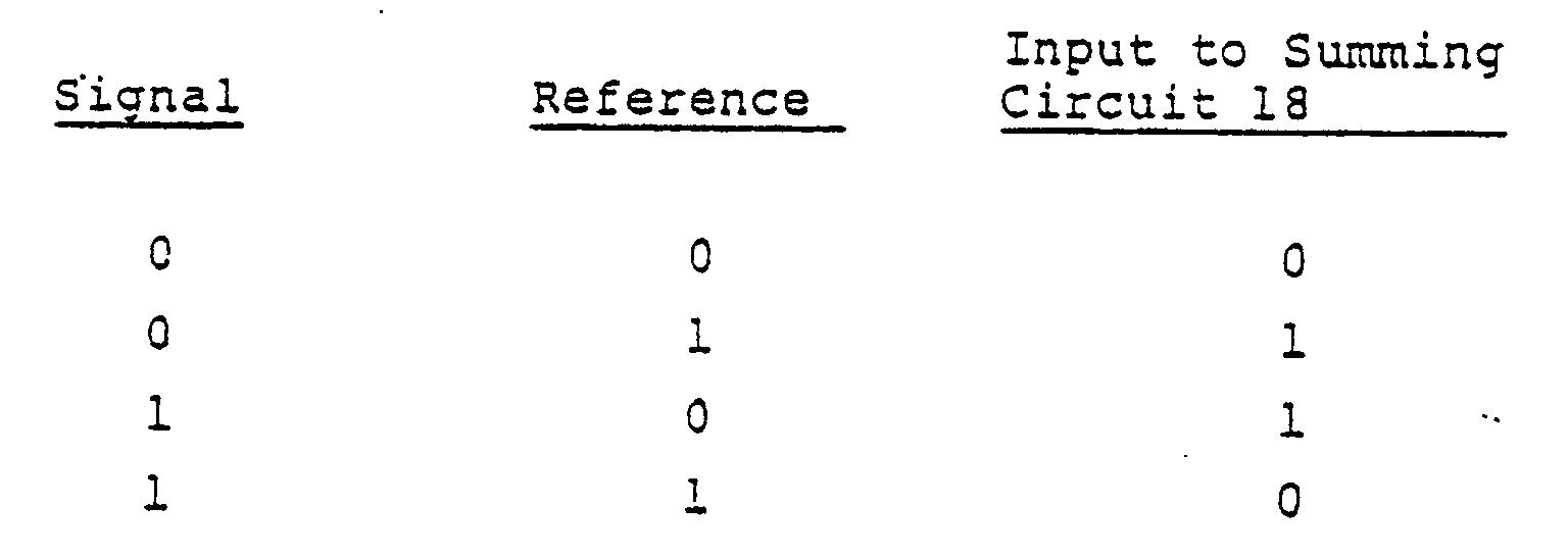
- As will be recognized, this is the truth table for an EXCLUSIVE-OR gate. If, due to logic circuit consideration, it is desired to have an output of logic "1" where the signal and reference bits are the same and to have a logic "0" output when the signal and reference bits are different, the EXCLUSIVE-OR gates could be followed by an inverter or NOT gate.
- Since each of the correlators 10 - 13 are constructed identically and, as a result, each have a summing circuit similar to summing
circuit 18, it would be possible to eliminate this separate summing circuit in the correlators by having a tree-like arrangement insumming circuit 14 wherein the outputs of each correlator are summed and then the resulting sums are further summed to provide the output I of Fig. 2. - The circuit arrangement of Fig. 1 employing the multiple-phase sampling scheme can be used to reduce the sampling losses associated with a discrete-time system mentioned hereinabove
- without any increases of circuitry complexity. It allows the use of slower speed correlator circuitry to be used to achieve a performance of N times the clock rate where N is the number of clock phases employed, which is equal to the number of input signals operated upon by the circuitry of Fig. 1.
- While I have described above the principles of my invention in connection with specific apparatus, it is to be clearly understood that this description is made only by way of example and not as a limitation to the scope of my invention as set forth in the objects thereof and in the accompanying claims.
Claims (13)
- An arrangement to provide an accurate time-of-arrival indication for N-received signals having a given time spacing there-between, where N is an integer greater to one, comprising:N signal channels, each responsive to a different one of said N signals, each of said N channels including:first means (1-9)to sample the associated one of said N signals at a given one of N-phase clocks, each of said N-phase clocks sampling a different one of said N signals at a predetermined different time uniformly spaced over a given time intervalland to delay the samples of the associated one of said N signals according to the given time spacing, andsecond means (10-13) coupled to said first means (1-9) to correlate the delayed samples of the associated one of said N signals the arrangement comprising further with a reference signal;third means (14) coupled to each of the second means (10-13) to integrate the correlated output signals of each of the second means (10-13) to provide said indication of said time-of-arrival of said N signals.
- An arrangement according to claim 1, wherein each of said first means (1, 2, 3, 4) includesa sampling circuit (1-5) to receive the associated one of said N signals and a given one of N- phase clocks, anda delay means (6-9) coupled to said sampling circuit (1-5) to time align the outputs of each of said sampling circuits.
- An arrangement according to claim 1 or 2, wherein each of said second means includesa digital correlator (10-13) coupled to an associated one of said first means (1-9) and clocked by said given one of said N-phase clocks.
- An arrangement according to claim 3, wherein each of said correlators (10-13) includesa first shift register (15) containing therein said reference signal,a second shift register (16) coupled to said associated one of said first means (1, 6), output signals of said associated one of said delay means (6) being clocked into said second shift register (16) by said given one of said N-phase clocks, andcomparison means (17) coupled to each stage of each of said first and second shift registers (15, 16) to compare the contents of associated stages of said first and second shift registers (15, 16) and produce a resultant output signal.
- An arrangement according to claim 4, wherein said comparison means (17, 18) includesa plurality of EXCLUSIVE-OR gates (17) equal in number to said associated stages of said first and second shift registers (15, 16) to enable comparison of the contents thereof, each of said gates producing at least a portion of said resultant output signal.
- An arrangement according to claim 5, wherein said comparison means (17, 18) further includesa first summing circuit (18) coupled to said plurality of EXCLUSIVE-OR gates (17) to provide said resultant output signal.
- An arrangement according to claim 5, wherein said comparison means (17, 18) further includesat least a first portion of said third means (14) coupled to said plurality of EXCLUSIVE-OR gates (17) to sum said portions of said resultant output signal to provide said resultant output signals.
- An arrangement according to claim 7, wherein said third means (14) includes a second portion coupled to each of said first portions to provide said indication of said time-of-arrival of said N signals.
- An arrangement according to claim 8, wherein each of said first portions of said third means (14) and said second portion of said third means (14) is a summing circuit.
- An arrangement according to claim 6, wherein said third means (14) includes a second summing circuit coupled to each of said first summing circuits (18) to provide said indication of said time-of-arrival of said N signals.
- An arrangement according to claim 4, wherein said third means (14) includes a summing circuit coupled to each of said comparison means (17) to sum each of said resultant output signals to provide said indication of said time-of-arrival of said N signals.
- An arrangement according to claim 3, wherein said third means (14) includes a summing circuit coupled to each of said digital correlators (10-13) to provide said indication of said time-of-arrival of said N signals.
- An arrangement according to claim 1 or 2, wherein said third means (14) includes a summing circuit coupled to each of said second means (10-13) to provide said indication of said time-of-arrival of said N signals.
Applications Claiming Priority (2)
| Application Number | Priority Date | Filing Date | Title |
|---|---|---|---|
| US06/512,810 US4559607A (en) | 1983-07-11 | 1983-07-11 | Arrangement to provide an accurate time-of-arrival indication for a plurality of received signals |
| US512810 | 1983-07-11 |
Publications (3)
| Publication Number | Publication Date |
|---|---|
| EP0131262A2 EP0131262A2 (en) | 1985-01-16 |
| EP0131262A3 EP0131262A3 (en) | 1986-12-03 |
| EP0131262B1 true EP0131262B1 (en) | 1991-03-27 |
Family
ID=24040674
Family Applications (1)
| Application Number | Title | Priority Date | Filing Date |
|---|---|---|---|
| EP84107845A Expired EP0131262B1 (en) | 1983-07-11 | 1984-07-05 | An arrangement to provide an accurate time-of-arrival indication for a plurality of received signals |
Country Status (5)
| Country | Link |
|---|---|
| US (1) | US4559607A (en) |
| EP (1) | EP0131262B1 (en) |
| JP (1) | JPS6051339A (en) |
| DE (1) | DE3484327D1 (en) |
| ES (1) | ES534189A0 (en) |
Families Citing this family (12)
| Publication number | Priority date | Publication date | Assignee | Title |
|---|---|---|---|---|
| US4660164A (en) * | 1983-12-05 | 1987-04-21 | The United States Of America As Represented By The Secretary Of The Navy | Multiplexed digital correlator |
| GB8628397D0 (en) * | 1986-11-27 | 1986-12-31 | Secr Defence | Digital correlator/structurator |
| FR2636758B1 (en) * | 1988-09-16 | 1994-09-09 | Platon Jean Pierre | METHOD AND SYSTEM FOR TRANSMITTING SIGNALS OVER THE AIR, IN PARTICULAR FOR A VEHICLE TO KNOW THE DISTANCE SEPARATING IT FROM A POTENTIAL OBSTACLE |
| US5218562A (en) * | 1991-09-30 | 1993-06-08 | American Neuralogix, Inc. | Hamming data correlator having selectable word-length |
| US6175848B1 (en) * | 1996-11-21 | 2001-01-16 | Trimble Navigation Limited | Variable accumulation correlators |
| US6182237B1 (en) | 1998-08-31 | 2001-01-30 | International Business Machines Corporation | System and method for detecting phase errors in asics with multiple clock frequencies |
| EP1282258A1 (en) * | 2001-08-02 | 2003-02-05 | Mitsubishi Electric Information Technology Centre Europe B.V. | Method and apparatus for synchronising receivers |
| EP1496085A1 (en) * | 2003-07-07 | 2005-01-12 | Total Petrochemicals Research Feluy | Heat-sealable and peelable polyethylene films |
| SG137726A1 (en) * | 2006-06-06 | 2007-12-28 | Sony Corp | A method and apparatus for measuring distance between a target and a receiver in a ranging system |
| JP5664869B2 (en) * | 2009-03-31 | 2015-02-04 | 日本電気株式会社 | Measuring apparatus, measuring system, measuring method, and program |
| FR2999298B1 (en) * | 2012-12-10 | 2015-01-09 | Sagem Defense Securite | METHOD AND DEVICE FOR DETERMINING THE TIME OF PROPAGATION OF A SURFACE ACOUSTIC WAVE FILTER |
| US10656244B2 (en) * | 2016-04-08 | 2020-05-19 | General Radar Corp. | Reconfigurable correlator (pulse compression receiver) and beam former based on multi-gigabit serial transceivers (SERDES) |
Family Cites Families (6)
| Publication number | Priority date | Publication date | Assignee | Title |
|---|---|---|---|---|
| US3887918A (en) * | 1973-05-09 | 1975-06-03 | Itt | Multi-level digital coincidence detection |
| US4007331A (en) * | 1975-08-13 | 1977-02-08 | Bunker Ramo Corporation | Apparatus for demodulation of relative phase modulated binary data |
| US4007330A (en) * | 1975-08-13 | 1977-02-08 | Bunker Ramo Corporation | Method and apparatus for demodulation of relative phase modulated binary data |
| US4209835A (en) * | 1978-07-21 | 1980-06-24 | Hughes Aircraft Company | Pulse repetition interval autocorrelator system |
| US4283767A (en) * | 1979-05-03 | 1981-08-11 | Raytheon Company | Multiple correlator reference processor |
| JPS598104B2 (en) * | 1979-08-08 | 1984-02-22 | 富士通株式会社 | Bit phase adjustment circuit |
-
1983
- 1983-07-11 US US06/512,810 patent/US4559607A/en not_active Expired - Lifetime
-
1984
- 1984-07-05 EP EP84107845A patent/EP0131262B1/en not_active Expired
- 1984-07-05 DE DE8484107845T patent/DE3484327D1/en not_active Expired - Lifetime
- 1984-07-10 JP JP59141566A patent/JPS6051339A/en active Granted
- 1984-07-11 ES ES534189A patent/ES534189A0/en active Granted
Also Published As
| Publication number | Publication date |
|---|---|
| ES8601599A1 (en) | 1985-10-16 |
| ES534189A0 (en) | 1985-10-16 |
| US4559607A (en) | 1985-12-17 |
| EP0131262A2 (en) | 1985-01-16 |
| JPS6051339A (en) | 1985-03-22 |
| DE3484327D1 (en) | 1991-05-02 |
| EP0131262A3 (en) | 1986-12-03 |
| JPH0577990B2 (en) | 1993-10-27 |
Similar Documents
| Publication | Publication Date | Title |
|---|---|---|
| US4559606A (en) | Arrangement to provide an accurate time-of-arrival indication for a received signal | |
| US6064688A (en) | CDMA synchronous acquisition circuit | |
| US4943974A (en) | Detection of burst signal transmissions | |
| US4559607A (en) | Arrangement to provide an accurate time-of-arrival indication for a plurality of received signals | |
| KR880004368A (en) | Sample Rate Conversion Circuit for Digital Data | |
| US5448245A (en) | Signal processing apparatus in radar | |
| US6621855B1 (en) | Scalable spread-spectrum signal detection and acquisition processor | |
| US3271742A (en) | Demodulation system | |
| US4259650A (en) | Sidelobe rejection filter | |
| US4722094A (en) | Digital rate detection circuit | |
| RU2165627C1 (en) | Doppler phase-meter of multifrequency signals | |
| US20060159206A1 (en) | Device and method for determining a time of arrival of a receive sequence | |
| RU2166772C1 (en) | Detector-measuring instrument of multifrequency signals | |
| KR940009238B1 (en) | Digital range correlation apparatus and method | |
| US4743969A (en) | Correlator | |
| SU585619A2 (en) | Device for synchronization with m-sequence | |
| US3622886A (en) | Synchronization system | |
| SU1716613A1 (en) | Device for synchronization of periodic code sequences | |
| SU1691938A1 (en) | Pulse sequence discriminator | |
| SU1401630A1 (en) | Phase synchronization device | |
| SU1370596A1 (en) | Device for measuring phase shift | |
| JPH0697775A (en) | Digital matched filter | |
| SU1197102A2 (en) | Autocorrelation meter of parameters of pseudorandom phase=shift keyed signal | |
| SU1137577A1 (en) | Frequency-manipulated signal demodulator | |
| SU1069182A1 (en) | Device for synchronizing correlative type receiver of pseudo-random signals |
Legal Events
| Date | Code | Title | Description |
|---|---|---|---|
| PUAI | Public reference made under article 153(3) epc to a published international application that has entered the european phase |
Free format text: ORIGINAL CODE: 0009012 |
|
| AK | Designated contracting states |
Designated state(s): DE FR GB |
|
| PUAL | Search report despatched |
Free format text: ORIGINAL CODE: 0009013 |
|
| AK | Designated contracting states |
Kind code of ref document: A3 Designated state(s): DE FR GB |
|
| 17P | Request for examination filed |
Effective date: 19870602 |
|
| 17Q | First examination report despatched |
Effective date: 19890208 |
|
| GRAA | (expected) grant |
Free format text: ORIGINAL CODE: 0009210 |
|
| AK | Designated contracting states |
Kind code of ref document: B1 Designated state(s): DE FR GB |
|
| REF | Corresponds to: |
Ref document number: 3484327 Country of ref document: DE Date of ref document: 19910502 |
|
| ET | Fr: translation filed | ||
| PLBE | No opposition filed within time limit |
Free format text: ORIGINAL CODE: 0009261 |
|
| STAA | Information on the status of an ep patent application or granted ep patent |
Free format text: STATUS: NO OPPOSITION FILED WITHIN TIME LIMIT |
|
| 26N | No opposition filed | ||
| REG | Reference to a national code |
Ref country code: GB Ref legal event code: IF02 |
|
| PGFP | Annual fee paid to national office [announced via postgrant information from national office to epo] |
Ref country code: GB Payment date: 20030702 Year of fee payment: 20 |
|
| PGFP | Annual fee paid to national office [announced via postgrant information from national office to epo] |
Ref country code: FR Payment date: 20030718 Year of fee payment: 20 |
|
| PGFP | Annual fee paid to national office [announced via postgrant information from national office to epo] |
Ref country code: DE Payment date: 20030731 Year of fee payment: 20 |
|
| PG25 | Lapsed in a contracting state [announced via postgrant information from national office to epo] |
Ref country code: GB Free format text: LAPSE BECAUSE OF EXPIRATION OF PROTECTION Effective date: 20040704 |
|
| REG | Reference to a national code |
Ref country code: GB Ref legal event code: PE20 |