EP0128412B1 - Anschlagdrucker mit Druckhammerauslösungskompensationsschaltung - Google Patents
Anschlagdrucker mit Druckhammerauslösungskompensationsschaltung Download PDFInfo
- Publication number
- EP0128412B1 EP0128412B1 EP84105834A EP84105834A EP0128412B1 EP 0128412 B1 EP0128412 B1 EP 0128412B1 EP 84105834 A EP84105834 A EP 84105834A EP 84105834 A EP84105834 A EP 84105834A EP 0128412 B1 EP0128412 B1 EP 0128412B1
- Authority
- EP
- European Patent Office
- Prior art keywords
- clock pulses
- circuit
- impact printer
- counter
- subscan
- Prior art date
- Legal status (The legal status is an assumption and is not a legal conclusion. Google has not performed a legal analysis and makes no representation as to the accuracy of the status listed.)
- Expired
Links
- 238000010304 firing Methods 0.000 title claims description 7
- 238000009825 accumulation Methods 0.000 claims description 4
- 230000003111 delayed effect Effects 0.000 claims description 4
- 230000001934 delay Effects 0.000 claims description 3
- 230000004044 response Effects 0.000 claims description 3
- 230000007274 generation of a signal involved in cell-cell signaling Effects 0.000 claims 1
- 230000001143 conditioned effect Effects 0.000 description 5
- 238000012937 correction Methods 0.000 description 4
- 238000010586 diagram Methods 0.000 description 4
- 230000007246 mechanism Effects 0.000 description 4
- 230000035508 accumulation Effects 0.000 description 3
- 230000003213 activating effect Effects 0.000 description 2
- 230000000903 blocking effect Effects 0.000 description 2
- 230000008859 change Effects 0.000 description 2
- 230000003750 conditioning effect Effects 0.000 description 2
- 230000033001 locomotion Effects 0.000 description 2
- 230000009467 reduction Effects 0.000 description 2
- 230000000630 rising effect Effects 0.000 description 2
- 108010076504 Protein Sorting Signals Proteins 0.000 description 1
- 238000003708 edge detection Methods 0.000 description 1
- 238000005259 measurement Methods 0.000 description 1
- 239000002184 metal Substances 0.000 description 1
- 238000000034 method Methods 0.000 description 1
- 230000003287 optical effect Effects 0.000 description 1
- 230000002441 reversible effect Effects 0.000 description 1
- 229910001220 stainless steel Inorganic materials 0.000 description 1
- 239000010935 stainless steel Substances 0.000 description 1
- 230000001360 synchronised effect Effects 0.000 description 1
Images
Classifications
-
- B—PERFORMING OPERATIONS; TRANSPORTING
- B41—PRINTING; LINING MACHINES; TYPEWRITERS; STAMPS
- B41J—TYPEWRITERS; SELECTIVE PRINTING MECHANISMS, i.e. MECHANISMS PRINTING OTHERWISE THAN FROM A FORME; CORRECTION OF TYPOGRAPHICAL ERRORS
- B41J9/00—Hammer-impression mechanisms
- B41J9/44—Control for hammer-impression mechanisms
- B41J9/50—Control for hammer-impression mechanisms for compensating for the variations of printer drive conditions, e.g. for compensating for the variation of temperature or current supply
Definitions
- This invention relates generally to high speed impact printers and, more particularly, to a circuit for varying the hammer firing times to compensate for variations in velocity as a character band moves along its path.
- Another important object of this invention is to provide a circuit that can accommodate both positive and negative changes from the nominal velocity of the moving type carrier and provide the necessary correction for hammer firing to produce improved registration.
- a further object of this invention is to provide a circuit for a printer having a moving type carrier in which changes in hammer firing delays can be determined for variations in nominal carrier velocity and which can be readily adapted to different nominal velocities.
- a still further object of this invention is to provide a circuit for determining delays for print hammers in a printer having a moving type carrier that is simpler, requires fewer components and is less expensive.
- control means enable the counter means for only the latter portion of each emitter or character timing signal period so that smaller counts are accumulated; the accumulated count can represent variations in the nominal type carrier velocity that indicate either a faster or slower velocity; and since the clock pulses are divided in frequency to provide the decrementing pulses, any dividing ratio can be easily preselected to provide the necessary compensation signal for the velocity variation.
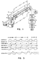
- Mechanism 10 comprises generally a moving metal band or belt 11, typically of stainless steel, having type characters 12 and timing marks 13,14 embossed or etched thereon; the band is supported for rotation about a pair of pulleys 15, 16, one of which is driven by a motor 17. Adjacent one side of band 11 between pulleys 15 and 16 lies a platen 18. Opposite the platen and adjacent the outside surface of band 11 is a horizontally movable ribbon 19 supported on a pair of spools 20, only one of which is shown, and a vertically movable recording medium, such as paper web 21, shown in phantom. Adjacent to the paper web are a plurality of selectively energizable print hammers 22 that can be individually and selectively actuated to impact paper web 21 against ribbon 19 and band 11 and, in turn, against platen 18.
- the impacts of the several hammers create an impression of the selected characters on the recording medium.
- the hammers are energized at appropriate times to produce an impression of the selected character as it comes into position while the band rotates continuously along its path.
- Ribbon 19 is reversible and also moves continuously in one direction or the other during printing.
- the band usually has a plurality of sets of characters formed on its surface and characters are selected for impact by the appropriate hammers by detecting a start or home pulse with transducer 23, which senses timing mark 14, then counting timing or emitter pulses sensed by transducer 24 sensing timing marks 13. This enables the determination of location of each of the band characters at any time.
- Engraved type elements 12 such as alphabetic or numeric characters or other graphic symbols, are uniformally spaced about band 11 but at a pitch which differs from the pitch of hammers 22. Due to this pitch differential, the type characters align as subgroups with subgroups of hammers 22 during band motion in accordance with the plurality of continuously recurring scan and subscan signal sequences.
- the scan/subscan principle of operation is well-known, and further detailed information can be obtained by reference to U.S. Patent 4 275 653, issued 30 June, 1981 to R. D. Bolcavage, et al.
- the print mechanism can have 168 print hammers for 168 print positions of a print line to be recorded on print medium 21 with the printed characters spaced 10 to 25.4mm (1 inch).
- Type band 11 may have 480 type elements 12 spaced at distances of 3.38mm (.133 inches), thereby providing four subscans per print scan. With this arrangement, a complete revolution of band 10 would produce 480 scans and 1 920 subscans.
- Timing marks 13 are equal in number with the type characters and have the same relative, uniform spacing. Therefore, marks 13 are aligned with type characters 12.
- Transducer 24 in sensing marks 13 produces emitter or scan pulses from amplifier 25.
- the scan pulses heretofore have then been directly transmitted to a frequency multiplier circuit such as a phase lock loop oscillator circuit 26 to convert the scan pulses to subscan pulses at a frequency equal to the number of subscan alignments of type elements 12 with hammers 22.
- a frequency multiplier circuit such as a phase lock loop oscillator circuit 26 to convert the scan pulses to subscan pulses at a frequency equal to the number of subscan alignments of type elements 12 with hammers 22.
- the phase lock loop oscillator circuit would generate four subscan pulses for each scan pulse generated by transducer 24 in response to each timing mark 13 sensed on band 11.
- the subscan pulses are combined subsequently with clock pulses to perform readouts from a print line buffer and band image buffer, neither of which is shown. Upon coincidence of values at these two units, an equality signal is effective to energize a corresponding hammer fire circuit to print that character.
- Print hammer selection is explained in greater detail in a European patent application, publication no. 98 375, published after the priority date of the present application.
- the hammer must be fired in advance of its actual impact point with the band because of the flight time required to move from a retracted position to meet the moving type character at the correct location.
- Hammer flight time can usually be relied on as being constant so that the time of release in advance of the impact point can be easily calculated for a predetermined band velocity.
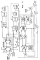
- the circuit represented by box 30 interposed between scan pulse amplifier 24 and the phase lock loop oscillator 26 that generates the subscan pulses. Circuit 30 measures the time elapsing between adjacent emitter pulses from sensed timing marks 13 and varies the time at which the oscillator circuit 26 initiates its series of four subscan pulses.
- Circuit 30 for compensating for variations in the nominal velocity of the band is shown in greater detail in Fig. 2, and related signal waveforms are shown in Fig. 3.
- An edge detector 31 is used for activating and synchronizing the compensating circuit for each emitter or scan pulse from sensor 24 (Fig. 1).
- the emitter pulses are fed to inverter 32, whose output is connected to the clock input for flip-flop 33 that is permanently conditioned to turn on.
- flip-flop 33 When flip-flop 33 turns on at the falling edge of the emitter pulse, it conditions companion flip-flop 34, which is clocked by signals from a continuous fast clock source 29, such as 10 MHz. The occurrence of one of the latter signals turns on flip-flop 34 and both outputs change.
- the on output clears main counter 35 to zero and resets blocking latch 36.
- Invert (Al) 41 resets delay latch 38 through OR Invert (01) 37 and conditions AI gate 40 through 0139. This latter circuit will be described hereinafter.
- the next succeeding clock signal turns flip-flop 34 off conditioning AI gate 41 and the clock signals start advancing main counter 35.
- the emitter pulses from sensor 24 (Fig. 1) are shown in waveform A, and the resulting signals from edge detector 34 are shown in waveform D of Fig. 3.
- Main counter 35 advances with the clock signals at the leading edge of the signal from edge detector 34 and the accumulating count produced by the clock signals is shown by the rising slope in waveform B of Fig. 3.
- Main counter 35 continues accumulating count until decode circuit 42 senses a preset value, at which time an output signal from the decoder occurs through delay 43.
- This delayed decode signal blocks further decoding by setting latch 36, sets delay latch 38, and delay extend latch 44 as seen in waveforms E and F of Fig. 3.
- These two latches when set provide conditioning levels to respective AI gating circuits 45 and 46 which, in turn, respectively enable either the count up or count down inputs of delay counter 47.
- AI gate 41 was conditioned by flip-flop 34, it permitted clock signals to pass through inverter 48 as activating signals to AI gate 45 and slow clock or frequency divider circuit 49. Clock signals from gate 45 are accumulated in delay counter 47.
- an emitter pulse has enabled main counter 35 to accumulate a value which activates a decode circuit to 42 to generate a check start pulse. This, in turn, activates delay latch 38 to enable delay counter 47 to count up for a portion of the emitter pulse period.
- Decode circuit 42 is connected to the stages of main counter 35 to produce its output only after the main counter has accumulated clock signals equal in time to approximately 97% or more of the nominal emitter period. Thereafter, the remainder of the emitter period is accumulated in delay counter 47. It will be seen from the description thus far that the count accumulated in delay counter 47 will reflect any variation in the emitter pulse period and will thus be a measure of the band velocity variation to be compensated.
- delay latch 38 When delay latch 38 is set by the next emitter pulse edge from 01 37, AI gate 45 is blocked and counter 47 is no longer advanced or incremented. However, AI gate 46, already having one input conditioned by delay extend latch 44 being on, has a second input conditioned by latch 38 being set off, and pulses from slow clock 49 begin to decrement or count down the value already accumulated.
- the slow clock is shown as a binary counter operating as a frequency divider. The desired frequency division is set by the connection of decode circuit 52. For example, the amount of delay per clock count can vary depending upon the band velocity. A reduction of 11:1 may be required at a high band velocity, whereas a reduction of 7:1 may be necessary at a slower velocity.
- Each slow clock pulse is delayed slightly at 53 to eliminate a race condition, and each delayed pulse clears the slow clock 49.
- delay counter 47 The decrementing of delay counter 47 is shown in waveform G in Fig. 3 as the downward slope from the peak count accumulation. Each peak value, of course, represents the relative length of the respective emitter period compared to a count representative of a nominal velocity represented by line 50.
- delay extend latch 44 is reset, blocking AI gate 46. This prevents passing further slow clock pulses and issues a signal through 01 39, and AI gate 40, already conditioned by a Not Disable signal to OR gate 55 and the phase lock loop oscillator 26 in Fig. 1. The oscillator will begin the generation of its series of subscan pulses.
- the period of each emitter pulse is measured by a main counter and delay counter acting together.
- the delay counter is effective for only a brief time, and its registered count is representative of the duration of only a brief portion of the emitter period. In the example given, its count may represent variations of up to plus or minus 3% in the nominal velocity of the type band.
- the delay counter is decremented at a slower preset rate of whatever is required to correspond to the nominal band velocity.
- the circuit of Fig. 2 has a precautionary secondary control at delay counter 47 which is decode circuit 56 that issues a signal upon detecting a predetermined high count limit. This limit signal is effective to reset delay latch 38 through 01 37 and allow the slow clock pulses from decoder 52 and delay 53 to begin decrementing the delay counter.
- the compensating circuit just described can be overridden by changing the Not Disable signal to the opposite level to disable decoder 42 and enable AI gate 57 to permit the phase lock loop oscillator to operate directly from the emitter pulses.
- the compensating circuit of the invention has the ability to adjust the timing of the phase lock loop oscillator when the band velocity is either slow or fast with respect to the nominal velocity. It will be seen from the diagrams of Fig. 3 that the terminal portion of each emitter period is represented by the accumulated count in the delay counter47. Count accumulations rising above line 50, representing the correct velocity, will indicate a slow band velocity and require a longer decrementing time to reach zero. Conversely, a count accumulation remaining below line 50 will indicate a band velocity faster than the nominal.
- line 58 from edge detector flip-flop 34 provides a control signal.
- delay extend latch 44 is set on so that its off output at OR Invert 39 has an input level that renders the occurrence of the edge detection signal from flip-flop 34 ineffective. If delay extend latch 44 is off at the occurrence of the pulse from flip-flop 34, then the latter pulse is effective to cause OR Invert 39 to produce a high level signal to AND 40 that provides a high level signal to OR Invert 55 that, in turn, produces a negative-going output to initiate operation of the phase lock loop.
Claims (8)
Applications Claiming Priority (2)
| Application Number | Priority Date | Filing Date | Title |
|---|---|---|---|
| US503915 | 1983-06-13 | ||
| US06/503,915 US4527920A (en) | 1983-06-13 | 1983-06-13 | Print hammer firing compensation circuit for printer velocity variation |
Publications (3)
| Publication Number | Publication Date |
|---|---|
| EP0128412A2 EP0128412A2 (de) | 1984-12-19 |
| EP0128412A3 EP0128412A3 (en) | 1987-10-21 |
| EP0128412B1 true EP0128412B1 (de) | 1991-02-06 |
Family
ID=24004064
Family Applications (1)
| Application Number | Title | Priority Date | Filing Date |
|---|---|---|---|
| EP84105834A Expired EP0128412B1 (de) | 1983-06-13 | 1984-05-23 | Anschlagdrucker mit Druckhammerauslösungskompensationsschaltung |
Country Status (4)
| Country | Link |
|---|---|
| US (1) | US4527920A (de) |
| EP (1) | EP0128412B1 (de) |
| JP (1) | JPS59232885A (de) |
| DE (1) | DE3484075D1 (de) |
Families Citing this family (8)
| Publication number | Priority date | Publication date | Assignee | Title |
|---|---|---|---|---|
| US4627344A (en) * | 1985-04-11 | 1986-12-09 | Centronics Data Computer Corp. | Impact printer with magnetic interaction compensation |
| WO1989000503A1 (en) * | 1987-07-21 | 1989-01-26 | Storage Technology Corporation | Control of printer functions via band id |
| US4854756A (en) * | 1987-08-03 | 1989-08-08 | Printronix, Inc. | Adaptive print hammer timing system |
| US5046413A (en) * | 1990-10-05 | 1991-09-10 | International Business Machines Corp. | Method and apparatus for band printing with automatic home compensation |
| US5547294A (en) * | 1991-12-19 | 1996-08-20 | Seiko Epson Corporation | Method and apparatus for controlling serial printer |
| CN112590402B (zh) * | 2020-12-11 | 2022-02-22 | 南阳柯丽尔科技有限公司 | 热敏打印机控制方法、装置、热敏打印机和介质 |
| CN112590401B (zh) * | 2020-12-11 | 2022-02-22 | 南阳柯丽尔科技有限公司 | 热敏打印机控制方法、装置、热敏打印机和介质 |
| CN112590400B (zh) * | 2020-12-11 | 2022-01-14 | 南阳柯丽尔科技有限公司 | 热敏打印机控制方法、装置、热敏打印机和介质 |
Family Cites Families (8)
| Publication number | Priority date | Publication date | Assignee | Title |
|---|---|---|---|---|
| US3656426A (en) * | 1969-05-08 | 1972-04-18 | Potter Instrument Co Inc | Apparatus for printing alphanumeric and binary code markings and comparison means therefor |
| US3575107A (en) * | 1969-06-02 | 1971-04-13 | Gen Electric | Underspeed and undervoltage protection for printer |
| US3752069A (en) * | 1971-07-01 | 1973-08-14 | Ibm | Back printer print line visibility control |
| FR2205003A5 (de) * | 1972-10-26 | 1974-05-24 | Honeywell Bull Soc Ind | |
| US3974765A (en) * | 1973-09-05 | 1976-08-17 | Compagnie Honeywell Bull (Societe Anonyme) | Apparatus for correcting the way in which print hammers strike |
| US3880075A (en) * | 1973-12-26 | 1975-04-29 | Burroughs Corp | Automatic chain identification method and apparatus |
| US4275653A (en) * | 1980-01-28 | 1981-06-30 | International Business Machines Corporation | Line printer system and method of operation with microprocessor control |
| US4425844A (en) * | 1982-06-23 | 1984-01-17 | International Business Machines Corporation | Home pulse compensation for multiple speed line printer |
-
1983
- 1983-06-13 US US06/503,915 patent/US4527920A/en not_active Expired - Fee Related
-
1984
- 1984-02-16 JP JP59026219A patent/JPS59232885A/ja active Granted
- 1984-05-23 DE DE8484105834T patent/DE3484075D1/de not_active Expired - Fee Related
- 1984-05-23 EP EP84105834A patent/EP0128412B1/de not_active Expired
Also Published As
| Publication number | Publication date |
|---|---|
| JPS59232885A (ja) | 1984-12-27 |
| DE3484075D1 (de) | 1991-03-14 |
| EP0128412A2 (de) | 1984-12-19 |
| JPH0448630B2 (de) | 1992-08-07 |
| EP0128412A3 (en) | 1987-10-21 |
| US4527920A (en) | 1985-07-09 |
Similar Documents
| Publication | Publication Date | Title |
|---|---|---|
| US6109721A (en) | Alignment system and process of automatically controlling bidirectional printing position of printhead in a serial printer | |
| US4220084A (en) | Document endorser apparatus | |
| EP0128412B1 (de) | Anschlagdrucker mit Druckhammerauslösungskompensationsschaltung | |
| JPH06320797A (ja) | 印刷方法 | |
| EP0026387B1 (de) | Verfahren zum Betrieb eines Anschlagdruckers mit einem Flugzeit- und Geschwindigkeitsdetektor | |
| JPH06344618A (ja) | 印刷方法 | |
| CA1110494A (en) | Printhead compensation arrangement for printer | |
| US4169991A (en) | Variable print speed control | |
| EP0659572B1 (de) | Drucker und Verfahren zur Steuerung desselben | |
| CA1189598A (en) | Printer | |
| US4167014A (en) | Circuitry for perfecting ink drop printing at varying carrier velocity | |
| US5803628A (en) | Printing apparatus including encoder pending | |
| US4522517A (en) | Encoder system for dot matrix line printer | |
| US4425844A (en) | Home pulse compensation for multiple speed line printer | |
| US4031992A (en) | Printing device | |
| US4167013A (en) | Circuitry for perfecting ink drop printing at nonlinear carrier velocity | |
| JPH06320762A (ja) | 印刷方法 | |
| US4185930A (en) | Print position control in a printer including a printer head mounted on a traveling carriage | |
| US3974765A (en) | Apparatus for correcting the way in which print hammers strike | |
| US6857799B2 (en) | Motor control method and apparatus, time recorder having same and impact type printing apparatus | |
| JPH0474192B2 (de) | ||
| US4328505A (en) | Ink jet printing apparatus | |
| JPS6134990B2 (de) | ||
| JP2674111B2 (ja) | 画像記録装置 | |
| JP2005178319A (ja) | 記録装置 |
Legal Events
| Date | Code | Title | Description |
|---|---|---|---|
| PUAI | Public reference made under article 153(3) epc to a published international application that has entered the european phase |
Free format text: ORIGINAL CODE: 0009012 |
|
| AK | Designated contracting states |
Designated state(s): DE FR GB |
|
| 17P | Request for examination filed |
Effective date: 19841123 |
|
| PUAL | Search report despatched |
Free format text: ORIGINAL CODE: 0009013 |
|
| AK | Designated contracting states |
Kind code of ref document: A3 Designated state(s): DE FR GB |
|
| 17Q | First examination report despatched |
Effective date: 19881230 |
|
| GRAA | (expected) grant |
Free format text: ORIGINAL CODE: 0009210 |
|
| AK | Designated contracting states |
Kind code of ref document: B1 Designated state(s): DE FR GB |
|
| REF | Corresponds to: |
Ref document number: 3484075 Country of ref document: DE Date of ref document: 19910314 |
|
| ET | Fr: translation filed | ||
| PLBE | No opposition filed within time limit |
Free format text: ORIGINAL CODE: 0009261 |
|
| STAA | Information on the status of an ep patent application or granted ep patent |
Free format text: STATUS: NO OPPOSITION FILED WITHIN TIME LIMIT |
|
| 26N | No opposition filed | ||
| PGFP | Annual fee paid to national office [announced via postgrant information from national office to epo] |
Ref country code: FR Payment date: 19940427 Year of fee payment: 11 |
|
| PGFP | Annual fee paid to national office [announced via postgrant information from national office to epo] |
Ref country code: DE Payment date: 19940513 Year of fee payment: 11 |
|
| PGFP | Annual fee paid to national office [announced via postgrant information from national office to epo] |
Ref country code: GB Payment date: 19951013 Year of fee payment: 12 |
|
| PG25 | Lapsed in a contracting state [announced via postgrant information from national office to epo] |
Ref country code: DE Effective date: 19960201 |
|
| PG25 | Lapsed in a contracting state [announced via postgrant information from national office to epo] |
Ref country code: FR Effective date: 19960229 |
|
| REG | Reference to a national code |
Ref country code: FR Ref legal event code: ST |
|
| REG | Reference to a national code |
Ref country code: FR Ref legal event code: ST |
|
| PG25 | Lapsed in a contracting state [announced via postgrant information from national office to epo] |
Ref country code: GB Effective date: 19960523 |
|
| GBPC | Gb: european patent ceased through non-payment of renewal fee |
Effective date: 19960523 |