EP0127892B1 - Verfahren und Einrichtung zur durch Grundperiode gesteuerten Sprachsignalverarbeitung - Google Patents
Verfahren und Einrichtung zur durch Grundperiode gesteuerten Sprachsignalverarbeitung Download PDFInfo
- Publication number
- EP0127892B1 EP0127892B1 EP84106307A EP84106307A EP0127892B1 EP 0127892 B1 EP0127892 B1 EP 0127892B1 EP 84106307 A EP84106307 A EP 84106307A EP 84106307 A EP84106307 A EP 84106307A EP 0127892 B1 EP0127892 B1 EP 0127892B1
- Authority
- EP
- European Patent Office
- Prior art keywords
- pitch
- memory
- read
- rate
- samples
- Prior art date
- Legal status (The legal status is an assumption and is not a legal conclusion. Google has not performed a legal analysis and makes no representation as to the accuracy of the status listed.)
- Expired
Links
- 238000000034 method Methods 0.000 title claims description 54
- 238000012545 processing Methods 0.000 title abstract description 12
- 230000015654 memory Effects 0.000 claims abstract description 59
- 230000008859 change Effects 0.000 claims abstract description 12
- 230000005236 sound signal Effects 0.000 claims description 19
- 230000006870 function Effects 0.000 claims description 11
- 238000013459 approach Methods 0.000 claims description 8
- 238000006243 chemical reaction Methods 0.000 claims description 7
- 238000000926 separation method Methods 0.000 claims description 5
- 238000005070 sampling Methods 0.000 claims description 4
- 230000004075 alteration Effects 0.000 claims 1
- 238000012544 monitoring process Methods 0.000 claims 1
- 230000006835 compression Effects 0.000 abstract description 35
- 238000007906 compression Methods 0.000 abstract description 35
- 230000008569 process Effects 0.000 description 48
- 239000000872 buffer Substances 0.000 description 28
- VLCQZHSMCYCDJL-UHFFFAOYSA-N tribenuron methyl Chemical compound COC(=O)C1=CC=CC=C1S(=O)(=O)NC(=O)N(C)C1=NC(C)=NC(OC)=N1 VLCQZHSMCYCDJL-UHFFFAOYSA-N 0.000 description 23
- 238000012986 modification Methods 0.000 description 12
- 230000004048 modification Effects 0.000 description 12
- 240000007320 Pinus strobus Species 0.000 description 11
- 239000011159 matrix material Substances 0.000 description 9
- 238000012546 transfer Methods 0.000 description 7
- 230000001360 synchronised effect Effects 0.000 description 6
- 238000007792 addition Methods 0.000 description 5
- 238000010586 diagram Methods 0.000 description 5
- 238000012360 testing method Methods 0.000 description 5
- 238000012217 deletion Methods 0.000 description 4
- 230000037430 deletion Effects 0.000 description 4
- 238000001514 detection method Methods 0.000 description 4
- 230000006872 improvement Effects 0.000 description 4
- 230000009191 jumping Effects 0.000 description 3
- 230000007704 transition Effects 0.000 description 3
- 238000013461 design Methods 0.000 description 2
- 230000000694 effects Effects 0.000 description 2
- 238000011156 evaluation Methods 0.000 description 2
- 238000005259 measurement Methods 0.000 description 2
- 230000003252 repetitive effect Effects 0.000 description 2
- 238000012552 review Methods 0.000 description 2
- 206010000210 abortion Diseases 0.000 description 1
- 230000003044 adaptive effect Effects 0.000 description 1
- 230000006399 behavior Effects 0.000 description 1
- 230000002457 bidirectional effect Effects 0.000 description 1
- 238000004364 calculation method Methods 0.000 description 1
- 230000001143 conditioned effect Effects 0.000 description 1
- 238000009795 derivation Methods 0.000 description 1
- 238000002955 isolation Methods 0.000 description 1
- 239000000463 material Substances 0.000 description 1
- 230000007246 mechanism Effects 0.000 description 1
- 238000007431 microscopic evaluation Methods 0.000 description 1
- 230000000737 periodic effect Effects 0.000 description 1
- 238000011160 research Methods 0.000 description 1
- 230000004044 response Effects 0.000 description 1
- 230000000717 retained effect Effects 0.000 description 1
- 230000000630 rising effect Effects 0.000 description 1
- 230000006403 short-term memory Effects 0.000 description 1
Images


Classifications
-
- G—PHYSICS
- G10—MUSICAL INSTRUMENTS; ACOUSTICS
- G10L—SPEECH ANALYSIS TECHNIQUES OR SPEECH SYNTHESIS; SPEECH RECOGNITION; SPEECH OR VOICE PROCESSING TECHNIQUES; SPEECH OR AUDIO CODING OR DECODING
- G10L21/00—Speech or voice signal processing techniques to produce another audible or non-audible signal, e.g. visual or tactile, in order to modify its quality or its intelligibility
- G10L21/04—Time compression or expansion
Definitions
- This invention relates to digital voice signa) processing to obtain pitch changing which processing is controlled by the pitch period of the voice signal being processed.
- the jump of the read pointer to its new address in memory is preselcted to utilize substantially all of the memory capacity that the initial differential between the write and read pointers is constant except for the small variation occasioned by the microscopic examination and adjustment made to provide a signal level match.
- Neuburg J. Acoustical Society of America, 63(2), Febr. 1978, pp. 624, 625) has suggested a new version of the original cut and splice method. Neuburg has proposed that for pitch lowering, the deletion (or in the case of pitch- raising, the repetition) of segments equal in length to an epoch, but regardless of where they started or ended, would produce good results.
- GB-A-2 098 032 discloses a pitch changer with glitch minimizer, in which a splice is made at a point of high auto-correlation, which by definition is at a point of high periodicity.
- the present invention solves the problem of providing an improved version of the pitch change cut and splice systems in which the discard intervals orthe repetition intervals for gap filling in compression and expansion respectively are controlled in accordance with a glottal pulse signal derived from the actual speech signal such that the benefits of the natural splicing of epochs can be realized in a system which can process tape recorded material at selectable playback speeds or in a system for real-time pitch shifting and which can be readily produced in high volume at low cost.
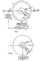
- a random access memory RAM 17 which receives the digitized samples of the audio input signal from an analog to digital converter 12 which digital words are written in memory sequentially by a write pointer 1.
- the memory is read out in the same sequence by a read pointer 2 and such digital words read from memory are converted in a digital to analog converter 16 to provide the audio output.
- the memory is under control of an address register 3 which is operated by control logic 4.
- Control logic 4 supplies a read rate signal f r which is fixed and write rate siganl f w which is equal to cf, where c is the compression ratio defined as unity for no pitch change and reproduction at the recorded rate and as a quantity greater than 1 for compression and less than 1 but greater than zero for expansion.
- the present addresses of the write and read pointers are used by control logic 4 to develop the operational control of the system.
- the difference between the present address locations indicated by the quantities F r (t) and F w (t) represents the angle 8, which in the representation of Fig. 1 is the angular spacing between the write and the read pointers 1 and 2.
- Also indicated in Fig. 1 are the quantities ⁇ min and 8 max defining a sector on opposite sides of the write pointer 1.
- the jump distance for the read pointer in accordance with the invention is always an integral number of pitch periods, but not pitch period synchronous.
- the jump does not need to be synchronized atthe glottal pulse but the period between glottal pulses is necessary to determine the magnitude of the jump along with other significant factors which determine the number of pulse periods the jump should be.
- a glottal pulse detector 32 develops a pulse signal output that is supplied to control logic 4 for this purpose.
- FIG. 2 the arrangement of Fig. 1 has been modified by adding a second read pointer 5 which moves at the speed of write pointer 1 with a fixed spacing therefrom represented by the angle ⁇ .
- the other modification shown in Fig. 2 is thatthe source of the audio signal is derived from the digitized audio input signal at the location of the second read pointer 5. This feature, as will be described, assures that a current value of glottal pulse period will be utilized by the system.
- FIG. 3A, 3B and 3C the architectural overview of a specific preferred embodiment digital system will be first described.
- the structure of this embodiment is divided into five functional blocks: Data Control, Address Generator, Access Control Processor, Jump Control, and Pitch Period Processor. These five elements, working in concert, control the data flow in a conventional digital Random Access Memory (RAM) 17, which is addressed sequentially in a continuous loop, and which provides the necessary short-term memory.
- RAM digital Random Access Memory
- Data Control is a straight-forward treatment for handling sampled data.
- the digitized data word has been established at 8-bits per sample, however the AID converter 12 and a digital to analog converter 16 are not necessarily restricted to be of the linear type, and may embody companding techniques to maximize the dynamic range of the established 8-bit data path.
- An Input Buffer 14 is for the general case of an analog-to-digital conversion that consumes a considerable portion of the available processing time. This element comprises a "mail-box" so that Data Control and Access Control need not wait upon one another. The Input Buffer 14 may not be required if the A/D converter is sufficiently fast to be idle when Access Control requires new data.
- an INPUT STROBE and an OUTPUT STROBE from Access Control operate buffers 14 and 15 but need not be necessarily regular. But in order to ensure regular sampling, the input sample should be in a fixed phase relationship with the WRITE CLOCK. Likewise, the output sample should be allowed to change only in a fixed phase relationship with the READ CLOCK.
- the Input Buffer 14 and the Output Buffer 15 provide this function.
- the depth of RAM 17 has been established at 512, 8-bit samples. Thus, a 9-bit address is required for each access to the RAM.
- a 9-bit sequential counter provides the RAM WRITE ADDRESS for the input sample.
- the counter is advanced under command of the signal WCNT, which may be the last item in the WRITE process flowchart (Fig. 4A), allowing nearly the full period of the WRITE CLOCK for its next address to settle.
- a 9-bit presettable counter 19 provides the READ ADDRESS and the non-sequential "intelligent" access to the output sample. It is under command of a combination of timing signals from Access Control and Jump Control.
- Either one of these two counter outputs is routed at different times to the RAM through the 9-bit parallel multiplexer called POINTER MUX 18.
- This functional block provides the detailed timing and decision logic for any and all access to data in the RAM 17. It is a single processor controlled by a processor clock 25 and time- shared by the two asynchronous processes READ and WRITE. Its function and its structure are not unlike the interrupt mechanism of a mini/ microcomputer.
- the idle state of the ACCESS CONTROL processor is denoted by the terminator WAIT 2.
- the processor is awaiting a service request from either the READ CLOCK or the WRITE CLOCK, or both simultaneously.
- a hardware flip/flop 23 is set to the appropriate condition corresponding to the process to be serviced, either READ or WRITE.
- TICK REGISTERS 21 and 22 and may be realized by almost any simple one-bit memory device. Their function is to provide one and only one service request for each period of the CLOCK (WRITE or READ) with which they are associated. Because they have memory, they also serve as a "mail-box" between their CLOCK and the ACCESS CONTROL PROCESSOR. Thus if ACCESS CONTROL is busy with a WRITE process when READ CLOCK requests new service, that request will still be waiting when the processor returns to "WAIT".
- JUMP CONTROL is not a separate processor. It is a collection of combinational logic that provides the arithmetic computation for producing a non-sequential (JUMP) next address or output access. It is under control of the ACCESS CONTROL processor and contains a minimum of control memory for coordinating its function under the two processes of READ and WRITE.
- the W/AP MUX 31 (called “MUX” in the FLOWCHART) is set to "W” and (+/-) is set (-). This permits the signed adder 26 to make a comparison of the WRITE POINTER and the READ POINTER. If logic decides to make a JUMP the READ pointer is moved (forward or back) by n ⁇ P where AP is the pitch period and n is an integer.
- ALERT DETECTION 27 examines the output of the signed adder and saves the decision in a JUMP Flip/Flop 29.
- the JUMP decision is different depending upon whether the system is set for COMPRESSION or EXPANSION. The details are shown in the FLOWCHART. The case of COMPRESSION or EXPANSION is determined by the +/- FLIP FLOP 28 which compares the sign of the difference quantity R-W. This evaluation is equivalent to determining whether to WRITE pointer has moved to within 8 mjn or 8 max of the READ pointer.
- This module measures the glottal pulse period and provides a constant access value of nAP for the magnitude of the jump.
- the central memory is a RAM 17, and the RAM requires an address and it delivers data, or it accepts data.
- Data Control treats the data, either in or out depending on whether it is writing or reading. Writing is at a certain address, which is provided by the write counter, and reading is from a read address.
- the two addresses have to be combined in a multiplexer POINTER MUX 18 in order to deliver a single address to the RAM because the program can only access the RAM, either read or write, but not both at the same time.
- An access control process coordinates the reading and the writing so that they are distinct. That processor is driven by asynchronous signals, i.e. the write clock and the read clock do not have to have any phase fixed relationship whatsoever.
- the selection of write or read is made by a flip flop 23's being held in an undefined state, where both its outputs are not distinct.
- the flip flop 23 is released to flop into one of its defined states to select one or the other, read or write.
- the WRITE and READ clocks are periodic.
- the leading edge of the write clock is detected by flip flop 21 and the leading edge of the read clock is being detected by flip flop 22 (TICK REGISTERS).
- Their Q outputs feed the set/reset inputs of a WRITE/READ flip flop 23, so the rising edge of clock will trigger the flip flop to make an decision to go to read or write.
- the input flip flops (the tick registers) are reset, so that there is a low on the set side and a low on the reset side of the read/write flip flop 23, and it is in a condition of so-called undefined state of its outputs, it really has not made a decision, as soon as either one or the other of the sets is released, then it will take up one or the other of the defined states. That causes it to select either the READ or the WRITE.
- This is like the so-called "fielder's choice", where the READ/WRITE flip flop is the fielder and has to serve both processes, the WRITE process and the READ process. If both come in at the same time it makes a fielder's choice. The process is so short that as soon as one is completed the other process will be acknowledged and serviced.
- PCSM PROCESSOR CLOCK STATE MACHINE
- the PCSM 25 provides a three-step function. It provides an initial delay, so that any process that had preceded the new process will have time to settle out. Then it allows one 4-bit nibble to happen, and finally a second 4-bit nibble which completes the process. Sometime during that process, because the access control processor knows what function it is performing-i.e. either read or write, but never the two simultaneously-it acknowledges the one that it is doing. It resets either 21 if 21 started it or 22 if 22 started it, but it does not acknowledge the other one. In short, when it has finished an operation, it acknowledges the one it did. If the operation that it was not doing is set in the meantime, it is immediately ready to perform that, immediately after the preceding one.
- the PCSM 25 has an asynchronous clock that can be started by either the write clock or the read clock transition of flip flops 21 or 22. When both are finished, the PCSM is set into its idle condition and no longer clocks. For each write clock transition and for each read clock transition there is guaranteed to be one and only one cycle of the PCSM.
- the 9-bit ripple counter 20 is maintaining the write address in a simple sequential fashion, one address after another, and after 512 addresses it returns to address 0. There is no reset for that counter. It simply produces a 9-bit address that rolls over by itself.
- the read counter 19 is a presettable counter which can be commanded to assume any desired preset number. That number is obtained from JUMP CONTROL as R ⁇ n ⁇ P, a 9-bit address for the preset of counter 19.
- the command to accept that preset is recognized by counter 19 when the LOAD CONTROL 30 is asserted and R counter RCNT has a leading edge.
- the load control in JUMP CONTROL provides the steering signal for counter 19 and is part of the read write/timing provided by the ACCESS CONTROL PROCESSOR. If the signal PRESET LOAD is asserted prior to an R count, the R ⁇ n ⁇ P preset is loaded into the presettable counter 19. That constitutes a jump.
- the 9- bit presettable counter is operated in very much the same manner as the counter 20. It runs under command of the R count signal RCNT which comes from the access control processor, so that prior to any read the counter 19 is incremented one address location.
- the ACCESS CONTROL PROCESSOR provides as its first order of business a delay time to allow the 9-bit presettable counter 19 time for its addresses to settle, and they must settle through the pointer MUX 18 into the RAM 17 prior to the data being strobed according.to the DATA CONTROL TIMING.
- the RAM output is allowed to assume its new analog value only on the leading edge of the signal from read clock number 11, so an output buffer 15 is provided that buffers during the time while the RAM is read out and during the time while that data has to be delivered to the output.
- the JUMP CONTROL determines the interval as an integral number of Pitch periods, nAP.
- the PITCH PERIOD PROCESSOR in a manner which will be described later, determines what that number is, and puts it on a bus we calls the nAP bus.
- a 9-bit number is thus continuously available on the nAP bus to determine the magnitude of the jump whenever a jump is needed. In the case of compression it must be a jump ahead into higher memory, in the case of expansion it must be a jump back into earlier memory, so the case of R+nAP and R-nAP provide respectively for compression and expansion.
- a 9-bit signed adder 26 adds the current address from the presettable counter 19 to the nAP number and provides a new address number at the R ⁇ n ⁇ P bus, for use when a jump is required.
- a multiplexer 31 w/AP MUX allows same 9-bit signed adder to be used not only to produce the new (after jump) address, but also to compare the current read address R with the current write address W, to determine when it is necessary to make a jump.
- Adder 26 continuously monitors each write address as it increments to compare that new write address to the current value of the read address.
- a signal from jump flip flop 29 is ordinarily in a relaxed condition (the W/AP MUX is normally set up to the W position) so that ALERT DETECTOR 27 can continually compare W against read R.
- W/AP MUX is normally set up to the W position
- ALERT DETECTOR 27 can continually compare W against read R.
- different algorithms are used to determine when it is necessary to jump.
- a single condition will allow determination of when it is necessary to jump but also of whether the mode is expansion or compression.
- Alert detector 27 monitors the output of adder 26 to determine when this alert condition has happened and when a jump must occur in order to avoid a discontinuity of the signal which would occur if write pointer coincided with the read pointer.
- load control 30 is signalled and it combines the read write timing signals R/W TIMING so that it asserts the load signale once, and once only, just ahead of the R count signal, so that only one jump is made at each time a jump requirement is detected.
- a plus minus flip flop 28 monitors the condition of the alert detector and thereby determines whether operation is in expansion or compression. For expansion it is necessary to assert the signal carry CY (which also feels the exclusive OR which is part of the 9-bit signed adder 26) to cause the 9-bit signed adder 26 now to assume the sign of a negative. In other words, it subtracts to produce R-nAP. That same flip flop 28 is commanded by ALERT DETECTOR 27 when it is necessary to be in the minus condition for a comparison between the read and the write addresses in order to assert jump flip flop 29.
- the amount of the jump, nAP is determined by the pitch period processor.
- This circuit is a combination of analog circuits and digital circuits.
- the input audio signal is applied to a glottal pulse detector 32.
- Detector 32 is a device that is predominantly a filter that tracks the incoming audio at varying speed according the value of C provided. If, as in a tape recorder application, there are variations in the playback speed, detector 32 tracks these, so that the parameters are normalized against the original recorded frequencies. It monitors the audio peaks to detect those peaks and advises the START/STOP transfer logic 36 that it has found each new peak.
- a 9-bit ripple counter block 33 is continuously counting at the write clock, WCNT. It transfers its latest count into 9-bit latch 34 and start counting again on receipt of each signal from START/STOP 36.
- the START/STOP transfer logic 36 receives another input called UPDATE INHIBIT out of the jump flip flop 29 that is necessary to keep the nAP number from changing simultaneously at the very time it is used to make the jump. In that event the transfer of the 9-bit ripple counter which is asynchronous with the W count would be held long enough so that it will not disturb the 9-bit latch 34 during the time of the read cycle when data must be available. After that, the update occurs.
- a limits detector 35 monitors the current value of the 9-bit ripple counter 33 as it counts up until it reaches a certain minimum number.
- This interval for a valid glottal pulse period corresponds to a pitch (i.e. fundamental frequency) range of 50 Hz and 100 Hz.
- the detected nAP will be close to the minimum limit (i.e. 10 ms) because of the high frequency of the detected peaks coming out of detector 32. That is, as soon as the limits detector 34 reaches that minimum number it is likely that a peak will come along and START/STOP 36 will load that number close to 10 ms into the 9-bit latch 34 and then start another cycle.
- a minimum number will be accumulated in 9-bit latch 34.
- a minimum value significantly less than 10 ms would result in a needlessly high processing rate, while increasing the maximum value is limited by the size of the memory. In this embodiment, the maximum was chosen to be half the memory size, which makes it convenient to determine the sign of the number out of the 9- bit signed adder 26.
- the system operates by program control as shown in Fig. 4A and 4B to make the jump as the write pointer approaches the read pointer.
- the flow chart is written as having two processors working on the blocks of WAIT 1 and WAIT 2.
- WAIT 1 stands for processor 1 and WAIT 2 for processor 2.
- the system has separate hardware. elements that are working in concert at the same time, so there is not a single processor. Their operation is described as distinct by using the processor notation WAIT 1 and WAIT 2 to show that there are processes that are going on simultaneously.
- the ACCESS CONTROL PROCESSOR of Fig. 3C is programmed as flow charted under WAIT 2. There are two competing processes, a write clock process (Fig. 4B) and a read clock process (Fig. 4A) that are waiting for processor number 2. Processor number 2 is devoted to doing the business of the random access memory which cannot read and write simultaneously.
- the decision block called ANY TICK? is a waiting loop used while the ACCESS CONTROL PROCESSOR is waiting for something to happen.
- ACCESS CONTROL has two tick registers 21, 22. When either tick register is set the tick decision block exits on the YES side into FLIP FLOP TO ONE ONLY, READ ELSE WRITE (corresponding to flip flop 23).
- the program signals the analog digital converter 12 to stay out of the input buffer Fig. 4B (BUFFER BUSY?). Then after a delay, it permits that buffer to clear had it been busy. This operation is CLEAR THE WRITE PROCESS TICK REGISTER. It can be done any time in this flow, but it is convenient to do it here.
- the input buffer is transferred to the random access memory. (In Fig. 3A the input buffer 14 is strobed by the input strobe and data is written in through the bidirectional I/0 line into RAM 17). Then the analog to digital converter, if it happens to be converting at that particular time, is cleared. The next step is to check POINTER ALERT.
- the output of the jump control 9-bit signed adder 26 is used to compare the read address against the write address to find out if the separation of the two pointers is collapsing. Most of the time the program will find that the pointers are not collapsing so the NO exit is taken. Then the only remaining order of business in the write process is to advance the write pointer, that is to incre- ' ment the 9-bit ripple counter 20. Then the program goes to WAIT 2. Now because the write process tick register was cleared, when the program comes back up to WAIT 2 it will hit the interrogation block ANY TICK? and there will not be a tick coming from the write clock. But a tick might have been recognised from the read clock. In that case ANY TICK YES goes to ONLY READ ELSE WRITE and selects READ because WRITE has been satisfied.
- the program strobes that output buffer to the DAC latch. This is shown in the upper right hand portion of the flow chart. The strobe occurs always on the leading edge of , the read clock. The last value that was resident in the buffer, when last read, is then transferred to the latch half of the digital analog converter 16. Because that read clock also triggers the tick register there will not be a read cycle that's occupying that buffer at the same time.
- the program After satisfying the read process the program will not do another read until the clock RCNT has gone low and then again high. If after the read process the write clock had left something in the tick register the program again would immediately follow through and do the write cycle.
- the pointer alert that is doing a comparison using the 9-bit signed adder 26 with the W/ ⁇ P MUX in the W position which it ordinairly is in, compares the read address with this latest write address. If the POINTER ALERT has signalled yes, (there is an impending collision of the two pointers), then alert detector 27 will have a signal asserted, and it will be used to set the jump flip flop 28.
- the way to determine the polarity is to examine the output of the 9-bit signed adder to determine the sign of R-W. All of the bits out of the 9-bit signed adder are examined to determine whether they are positive or negative. If they are small and positive then it must be because the pointers are collapsing in that particular direction-i.e. the case of compression. If they are small and negative, it must be because the pointers are collapsing in a direction that means to expansion. Even though the sign is determined, there is no jump because the program is in the write process. The program sets the jump flip flop and goes over to the read process toward the condition block to interrogate in the read process whether the JUMP flip flop is set.
- the program interrogates the jump flip flop and since it is set, it takes the branch. This will jump the read pointer which takes R to R+ or -nAP, the plus or minus being determined by the plus or minus flip flop block 28, which had been set in compression during the write process. Making the jump clears the jump flip flop to acknowledge the fact that the write process had called for a jump which was executed. Thus the program jumps only once, until the condition happens again.
- the W/AP MUX 31 is returned to its normal condition in the write position, and the plus minus flip flop 28 is cleared to its normal condition, being minus.
- the two conditions of being in the minus position and being in the W position are always needed to compare W against R to determine if a jump is required.
- the last order of business in Fig. 4A is to steer the pointer MUX to its normal position, i.e. WRITE.
- the program for analog to digital converter 12 is shown under WAIT 1 in Fig. 4B.
- the tick register 21 monitors the write clock. If the write clock leading edge happens at this time, this processor can recognize it in the same manner that WAIT 2 did. The first thing it does is clear this tick register and that causes the conversion from analog to digital. To determine where to store that data it must examine whether or not input buffer 14 is busy, because the process of WAIR 2 could be accessing it at the same time. If buffer 14 is free to be used then BUFFER BUSY? is NO. This takes the conversion from the analog to digital converter 12 and puts it into the input buffer 14. The program immediately goes back and starts another conversion unless WAIT 2 process signals it to stay out of buffer.
- That same audio analog signal that is about to be converted to digital is being used by the analog pitch period detector 32 to decide whether or not there is a start of a pitch period, by detecting a glottal pulse.
- WAIT 3 another process (which is nothing more than a counter and a few gates) is counting the interval between glottal pulses of the audio input.
- the program disables a peak or "P" counter (comprised of a 9- bit RIPPLE counter 33, START/STOP TRANSFER LOGIC 36 and LIMITS DETECTOR 35) to stop the input pulses and set the count to zero, and then it waits for a new glottal pulse to appear.
- the counter 33 is reset to a starting condition of zero.
- the last value of the pitch period that was counted is not lost because it can be resident in 9- bit latch 34.
- the program exits the START OF PITCH PERIOD in the yes branch and enables the peak counter. Enabling the peak counter allows the W counts WCNT to come in on the right hand side of the 9-bit ripple counter 33.
- the system monitors the glottal pulses and each count advances the counter, P becomes P+1.
- the limit detector 35 checks whether or not the high limit count is overrun, that is, if the count is greater than 384 which is about 3/4 the size of the memory and equivalent to roughly 20 ms.
- the program asks whether or not the end of pitch period has happened. If there is a glottal pulse, the count is stopped and the program exits via the yes branch and then examines the number in the P counter to see if it is greater than 95. This is an arbitrary limit that is set, equivalent to the 10 ms minimum limit. If the number is greater than that very small minimum then it is called a good pitch period because it had to be less than or equal to 384 and it had to be greater than 95 which constitutes good pitch period (i.e. a voiced pitch). Then the program asks if the jupm flip flop is set. If the jump flip flop is set latch 34 is not changed because the read cycle may be using it at the same time.
- the read cycle is not about to use the nAP that is resident in the 9-bit latch 34 so ⁇ P BUFFER is updated. In that case the number from the 9-bit ripple counter 33 is transferred to the 9-bit holding latch 34 and that ends that cycle.
- the program continues to loop and increment the P counter on each new write count.
- the program counts the number of write cycles between glottal pulses, and this interval when found is loaded into the 9-bit latch 34.
- FIG. 5 shows only enough of Fig. 3 to illustrate the changes made for this improvement.
- This embodiment addresses the problem of the large time delay between the detection of glottal pulses and the use of this information for the Read Pointer jumps. It improves operation by providing an auxiliary Read Pointer in fixed relative position to the write pointer and used solely for the purpose of providing data to the glottal Pulse Detector 32.
- This data from read pointer R2 is read out of memory through an additional DAC 37, buffered by an additional output buffer 36. It should be noted that depending upon the speed capabilities of a typical DAC, a single DAC may serve in a multiplexed capacity to provide the secondary "R2 Analog Data".
- an additional strobe timing signal is required from the Access Control Processor.
- This signal called R2 Strobe is generated by Access Control Processor in response to a request for Access to the RAM derived from WRITE CLOCK ODD.
- WRITE CLOCK 10 is necessarily doubled in frequency for this refinement.
- a divide-by-two flip/flop 38 delivers two alternating signals. One of them, WRITE CLOCK EVEN, is used to signal the input A/D converter 12 in the same manner and at the same frequency as was used for the system of Fig. 3. Access to the RAM for writing the digital data into memory is synchronized from this signal in a manner similar to the basic system.
- the new signal WRITE CLOCK ODD gains access to the RAM by way of the Access Control Processor to cause a READ Process to occur in between each WRITE process, and so this new READ process occurs at the same controlled rate as the WRITE processing.
- the WRITE aspect of WRITE Processing is the same as in the basic system, however a new READ aspect is added so that the Audio Input signal can effectively be shifted along the time-axis before being applied to the Glottal Pulse Detector 32.
- an additional DAC function is needed for this refinement.
- Such additional function may be provided explicitly in the additional DAC 37 or it may be derived implicitly by suitable multiplexing of DAC 16 of Fig. 3 with subsequent analog demultiplexing.
- the 9-bit RIPPLE COUNTER 20 is the same Write Pointer Counter as in the basic system.
- a new offset structure comprised of a 4-bit Adder 39 and W/R2 Selection Multiplexer 40 provides for the time-axis shift.
- an "offset code" of 128 is shown as an input to the 4-bit Adder 39.
- This number may be any number that can be represented with the upper 4-bits of a 9-bit code, 128 happesn to represent one-quarter of the 512 possible WRITE addresses.
- the smallest possible number for a 4- bit offset code is 32, representing 6-1/4% of the depth of the data memory. Other codes in incre- . ments of 6-1/4% are possible.
- the secondary R2 Analog Data may be selected to be read out of memory either ahead of the WRITE Pointer or behind the WRITE Pointer depending upon the phase relationship of timing signals OFFSET SELECT and WRITE CLOCK EVEN. If OFFSET SELECT is asserted to select the 4-bits, from 4-bit Adder 39 at the same time as WRITE EVEN causes data to be written into memory, while READ Aspect R-2 Strobe occurs when OFFSET SELECT is unasserted to select the 4-bits directly from counter 20, then the R2 Analog Data will lag behind the Audio INput by the amount of OFFSET CODE.
- COMPRESSION/EXPANSION DISCRIMINATOR 45 This lock block compares the writing rate against the reading rate and so is able to assert a logic signal "COMP" when the writing rate exceeds the reading rate. ACCESS CONTROL PROCESSOR is thus able to make use of this information in deciding which phase relationship to apply to OFFSET SELECT.
- addresses derived from counter 20 are efefctively the same for WRITE CLOCK EVEN and WRITE CLOCK ODD, providing a condition of zero offset regardless of the value of "OFFSET CODE". It is this condition of zero offset that is desirable for the case of Expansion, wherein the READ Pointer jumps backward away from the WRITE Pointer, jumping over data that has just been evaluated for its pitch-period.
- the READ Pointer tends to lag behind the WRITE Pointer and this lag becomes progressively greater until it becomes necessary to jump ahead because the full size of the circular store is filled and the WRITE Pointer will soon overrun the READ Pointer resulting in an uncontrolled "jump” and a consequential indeterminate splice of the output data. Accordingly, when a jump is taken just slightly before this overrun condition and it is taken only by the amount of "nAP", the resulting READ Pointer will still likely be deep into data memory. In fact, with this "Jump-On-Necessity" Logic, the READ Pointer manages to just stay ahead of the WRITE Pointer in the circular store.
- An embodiment of the invention affords two distinct features either for the Basic System of Fig. 3 or for a Basic System refined according to R2 (W) as in Fig. 5.
- the modifications of Fig. 3 used to implement these features are shown in Fig. 6.
- the first feature affords a means to obtain a multiplicative value for nAP, wherein AP comes from a measurement between exactly two glottal pulses and "n" is derived from the second feature.
- the second feature affords a means to control the "keep interval", the interval between jumps which becomes more important at higher values of compression "C" when the WRITE POINTER speeds away from the READ POINTER so fast that jumps are necessary so often that the READ POINTER is never able to deliver a contiguous segment that is long enough to guarantee that it contains at least one glottal pulse.
- Such higher compression ratios dictate the use of larger discard segments to insure that the keep segments will be of adequate length; however, at lower compression ratios, shorter discard segments may be preferable.
- Matrix ROM (Read-Only-Memory) 42 provides a means to adapt a large memory for purposeful full exploitation for large C and for purposeful partial exploitation for C more nearly unity.
- the absolute value of jump equivalent to the discard segment can be the design objective, because "AP" is part of the Matrix input.
- READ/WRITE FREQUENCY DISCRIMINATOR 44 compares the writing rate against the Reading rate and provides a 3-bit binary measure of compression "C". Thus C 2 output represents compression, C O - 5 represents expansion and C 1 is normal playback with no pitch change.
- a "AP" counter provides a frequently updated 9-bit binary number representing the interval of address locations between glottal pulses. Together these 12-bits provide a look-up address for Matrix ROM 42.
- Combinational Logic on the 12-bit addresses AP and C can be used to reduce this memory requirement.
- AP Counter stores its most recent measurement in 9-bit ⁇ P BUFFER 46, and each time it does so it signals successive ADDITION SEQUENCER 41 that new data is available.
- the successive ADDITION SEQUENCER receives a synchronizing start signal END OF READ CYCLE. If new data is available from the ⁇ P counter, the SUCCESSIVE ADDITION SEQUENCER will begin to perform "n” successive additions and will complete its operations before the next READ-CYCLE when "nAP" may be required.
- a RESET signal is first sent to a 9- bit nAP store 43 to clear it to zero. This zero appears on a 9-bit adder 40 together with the new ⁇ P from the ⁇ P counter.
- a strobe signal is then issued to nAP STORE 43 from the sequencer 41 so that it takes the sum of ⁇ P and zero.
- n(P, C) ⁇ 2 successive strobes are issued, with only a short settling time required between strobes.
- the architecture for this refinement is the same architecture as that of Figs. 3 and 4, the only modification's necessary are contained in the timing signals that are generated by the ACCESS CONTROL PROCESSOR.
- the modification may be thought of as producing a "trial jump" between each and every READ ACCESS, so that a second virtual ALERT POINTER is created, running at the READ rate but running ahead of the READ POINTER by an amount nAP. Then the ALERT DETECTOR 27 instead of operating on the quantity "R-W”, operates on the quantity "R+nAP-W”.
- the criteria for ALERT (when a jump is to be taken) then becomes not a JUMP-OF-NECESSITY but rather a JUMP-ON-OPPORTUNITY.
- the modification need only apply to the case of compression.
- the case of Expansion remains unchanged, its ALERT Logic is still the Jump-of-Necessity but because its READ rate tends to overtake the WRITE POINTER, the two pointers tend to maintain a close separation with the READ POINTER only in shallow memory.
- the Pitch-Period information obtained from the Audio INput (essentially equivalent to the information being written into the memory by the WRITE POINTER) can be used for determining the jump distance without introducing an error due to spatial separation in the memory.
- the Pitch-Period being extracted from the AUDIO INput is that corresponding to the signal information stored in shallow memory. This is generally a desirable feature because it means that when the Pitch-Period changes the speech waveform that belongs to that change is in recent memory. If a jump is taken over that same waveform it will produce a good splice, since the Pitch-Period information used is that of the signal actually jumped over. But if the READ POINTER is allowed to sink deep into memory the waveforms that it jumps over have been measured for Pitch-Period at a much earlier time and if the Pitch-Period is changing and is being continuously updated, the appropriate nAP for the jump is no longer available.
- the READ Access of Fig. 3 is left unmodified, however the WRITE Access is expanded to perform the Trial Jump and the ALERT testing.
- WRITE Access not only is data written into memory but a Trial Jump is commanded of the READ address counter.
- the W/ ⁇ P Multiplexer 31 is reset to "W" and "+/-" to "-" so that a comparison can be made between the trial jump and the current WRITE Address counter, which is the ALERT test.
- the result of the test determines whether or not the trial jump will be retained as an actual jump.
- the READ Address Counter is either commanded to return to its original value or simply left in the "R+n ⁇ P" condition, thus constituting a jump.
- the ALERT test indicates that the Trial Jump should be reneged, so a second command is issued after having returned the W/AP Multiplexer 31 to ⁇ P.
- the last item of business in the expanded WRITE Access is to update the NAP Counter. It is important to note that the nAP that is used ifor the Trial Jump is not changed before it will again be used to renege the jump.
- the criteria for the ALERT Test to decide to retain the Trial Jump is simply that there is "room” to Jump. If the Trial Jump causes the ALERT POINTER (R+N P) to exceed the WRITE POINTER then it is not yet time to retain the jump, and the Trial Jump is reneged. This strategy ensures that the READ POINTER sinks no deeper into memory that it has to. As soon as it has sunk back far enough that it can jump forward by n P without overtaking the WRITE POINTER, it does so. The result is that the READ POINTER operates in the same shallow memory for both the case of Expansion and now also for the case of compression.
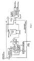
- FIG. 7 An alternate to the embodiment of Fig. 6 is shown in Fig. 7.
- the system of Fig. 7 provides all of the features of Fig. 6 and adds the additional ability to provide predetermined default constants for nAP under certain specified conditions.
- the values tabled in the MATRIX ROM (50) are simply AP multiplied by the most advantageous integer n for the C rate. Thus the multiplication is already taken care of when the Matrix 50 is consulted in real time.
- the values tabled can be "default" values that have been determined to be most appropriate for the particular C rate.
Landscapes
- Engineering & Computer Science (AREA)
- Computational Linguistics (AREA)
- Quality & Reliability (AREA)
- Signal Processing (AREA)
- Health & Medical Sciences (AREA)
- Audiology, Speech & Language Pathology (AREA)
- Human Computer Interaction (AREA)
- Physics & Mathematics (AREA)
- Acoustics & Sound (AREA)
- Multimedia (AREA)
- Analogue/Digital Conversion (AREA)
- Reduction Or Emphasis Of Bandwidth Of Signals (AREA)
- Selective Calling Equipment (AREA)
- Compression, Expansion, Code Conversion, And Decoders (AREA)
- Signal Processing For Digital Recording And Reproducing (AREA)
- Input Circuits Of Receivers And Coupling Of Receivers And Audio Equipment (AREA)
Claims (19)
Priority Applications (1)
| Application Number | Priority Date | Filing Date | Title |
|---|---|---|---|
| AT84106307T ATE48714T1 (de) | 1983-06-03 | 1984-06-01 | Verfahren und einrichtung zur durch grundperiode gesteuerten sprachsignalverarbeitung. |
Applications Claiming Priority (2)
| Application Number | Priority Date | Filing Date | Title |
|---|---|---|---|
| US50063283A | 1983-06-03 | 1983-06-03 | |
| US500632 | 1983-06-03 |
Publications (2)
| Publication Number | Publication Date |
|---|---|
| EP0127892A1 EP0127892A1 (de) | 1984-12-12 |
| EP0127892B1 true EP0127892B1 (de) | 1989-12-13 |
Family
ID=23990269
Family Applications (1)
| Application Number | Title | Priority Date | Filing Date |
|---|---|---|---|
| EP84106307A Expired EP0127892B1 (de) | 1983-06-03 | 1984-06-01 | Verfahren und Einrichtung zur durch Grundperiode gesteuerten Sprachsignalverarbeitung |
Country Status (7)
| Country | Link |
|---|---|
| EP (1) | EP0127892B1 (de) |
| JP (1) | JPS60501477A (de) |
| AT (1) | ATE48714T1 (de) |
| AU (1) | AU3063584A (de) |
| CA (1) | CA1211569A (de) |
| DE (1) | DE3480748D1 (de) |
| WO (1) | WO1984004989A1 (de) |
Families Citing this family (4)
| Publication number | Priority date | Publication date | Assignee | Title |
|---|---|---|---|---|
| GB2191916A (en) * | 1986-06-10 | 1987-12-23 | Alan Wyn Davies | Sound processing and reproduction system |
| GB2229068A (en) * | 1989-02-28 | 1990-09-12 | Univ Open | Playing back recorded speech at faster rate with pitch reduction |
| DE4425767C2 (de) * | 1994-07-21 | 1997-05-28 | Rainer Dipl Ing Hettrich | Verfahren zur Wiedergabe von Signalen mit veränderter Geschwindigkeit |
| US6584437B2 (en) | 2001-06-11 | 2003-06-24 | Nokia Mobile Phones Ltd. | Method and apparatus for coding successive pitch periods in speech signal |
Family Cites Families (11)
| Publication number | Priority date | Publication date | Assignee | Title |
|---|---|---|---|---|
| US3104284A (en) * | 1961-12-29 | 1963-09-17 | Ibm | Time duration modification of audio waveforms |
| FR1415553A (fr) * | 1964-05-26 | 1965-10-29 | Ibm France | Perfectionnements aux systèmes d'analyse de la voix |
| US3949175A (en) * | 1973-09-28 | 1976-04-06 | Hitachi, Ltd. | Audio signal time-duration converter |
| US3872503A (en) * | 1974-01-23 | 1975-03-18 | Westinghouse Electric Corp | Elimination of transients in processing segments of audio information |
| US4020291A (en) * | 1974-08-23 | 1977-04-26 | Victor Company Of Japan, Limited | System for time compression and expansion of audio signals |
| JPS5126507A (de) * | 1974-08-30 | 1976-03-04 | Victor Company Of Japan | |
| US3950617A (en) * | 1974-09-09 | 1976-04-13 | The United States Of America As Represented By The Secretary Of The Navy | Helium speech unscrambler with pitch synchronization |
| US4121058A (en) * | 1976-12-13 | 1978-10-17 | E-Systems, Inc. | Voice processor |
| JPS56126898A (en) * | 1980-03-12 | 1981-10-05 | Sony Corp | Voice pitch converter |
| JPS57135408A (en) * | 1981-02-16 | 1982-08-21 | Matsushita Electric Ind Co Ltd | Time base converter of sound signal |
| US4464784A (en) * | 1981-04-30 | 1984-08-07 | Eventide Clockworks, Inc. | Pitch changer with glitch minimizer |
-
1984
- 1984-05-30 WO PCT/US1984/000848 patent/WO1984004989A1/en not_active Ceased
- 1984-05-30 AU AU30635/84A patent/AU3063584A/en not_active Abandoned
- 1984-05-30 JP JP59502358A patent/JPS60501477A/ja active Pending
- 1984-06-01 AT AT84106307T patent/ATE48714T1/de not_active IP Right Cessation
- 1984-06-01 DE DE8484106307T patent/DE3480748D1/de not_active Expired - Fee Related
- 1984-06-01 EP EP84106307A patent/EP0127892B1/de not_active Expired
- 1984-06-01 CA CA000455659A patent/CA1211569A/en not_active Expired
Also Published As
| Publication number | Publication date |
|---|---|
| CA1211569A (en) | 1986-09-16 |
| JPS60501477A (ja) | 1985-09-05 |
| ATE48714T1 (de) | 1989-12-15 |
| AU3063584A (en) | 1985-01-04 |
| EP0127892A1 (de) | 1984-12-12 |
| WO1984004989A1 (en) | 1984-12-20 |
| DE3480748D1 (de) | 1990-01-18 |
Similar Documents
| Publication | Publication Date | Title |
|---|---|---|
| US4700391A (en) | Method and apparatus for pitch controlled voice signal processing | |
| US4121058A (en) | Voice processor | |
| US4375083A (en) | Signal sequence editing method and apparatus with automatic time fitting of edited segments | |
| US3803363A (en) | Apparatus for the modification of the time duration of waveforms | |
| US5386493A (en) | Apparatus and method for playing back audio at faster or slower rates without pitch distortion | |
| US4486900A (en) | Real time pitch detection by stream processing | |
| US5216744A (en) | Time scale modification of speech signals | |
| US4792975A (en) | Digital speech signal processing for pitch change with jump control in accordance with pitch period | |
| US4586027A (en) | Method and system for data compression and restoration | |
| EP0714089B1 (de) | CELP-Koder und -Dekoder und Verfahren dazu | |
| EP0127892A1 (de) | Verfahren und Einrichtung zur durch Grundperiode gesteuerten Sprachsignalverarbeitung | |
| Rosenthal et al. | A multiline computer voice response system utilizing ADPCM coded speech | |
| US5218640A (en) | Voice recording and reproducing apparatus | |
| US4813075A (en) | Method for determining the variation with time of a speech parameter and arrangement for carryin out the method | |
| CA2134308C (en) | Audio synthesizer time-sharing its first memory unit between two processors | |
| KR100236686B1 (ko) | 데이터 샘플열 액세스 장치 | |
| US5710386A (en) | Method and apparatus for efficiently controlling access to stored operation control data and tone forming data | |
| US4301333A (en) | Speech compression | |
| EP0376342B1 (de) | Datenverarbeitungsvorrichtung für ein elektronisches Musikinstrument | |
| JP2700937B2 (ja) | 早聞き装置 | |
| US7274967B2 (en) | Support of a wavetable based sound synthesis in a multiprocessor environment | |
| US4620316A (en) | Speech recognition system | |
| JP2576615B2 (ja) | 処理装置 | |
| JPS62994A (ja) | Pcm音声信号記憶装置 | |
| JPH04361296A (ja) | 波形データ圧縮方法及び装置ならびに再生装置 |
Legal Events
| Date | Code | Title | Description |
|---|---|---|---|
| PUAI | Public reference made under article 153(3) epc to a published international application that has entered the european phase |
Free format text: ORIGINAL CODE: 0009012 |
|
| AK | Designated contracting states |
Designated state(s): AT BE CH DE FR GB IT LI LU NL SE |
|
| 17P | Request for examination filed |
Effective date: 19850524 |
|
| 17Q | First examination report despatched |
Effective date: 19861125 |
|
| GRAA | (expected) grant |
Free format text: ORIGINAL CODE: 0009210 |
|
| AK | Designated contracting states |
Kind code of ref document: B1 Designated state(s): AT BE CH DE FR GB IT LI LU NL SE |
|
| PG25 | Lapsed in a contracting state [announced via postgrant information from national office to epo] |
Ref country code: SE Effective date: 19891213 Ref country code: LI Effective date: 19891213 Ref country code: IT Free format text: LAPSE BECAUSE OF FAILURE TO SUBMIT A TRANSLATION OF THE DESCRIPTION OR TO PAY THE FEE WITHIN THE PRESCRIBED TIME-LIMIT;WARNING: LAPSES OF ITALIAN PATENTS WITH EFFECTIVE DATE BEFORE 2007 MAY HAVE OCCURRED AT ANY TIME BEFORE 2007. THE CORRECT EFFECTIVE DATE MAY BE DIFFERENT FROM THE ONE RECORDED. Effective date: 19891213 Ref country code: CH Effective date: 19891213 Ref country code: AT Effective date: 19891213 |
|
| REF | Corresponds to: |
Ref document number: 48714 Country of ref document: AT Date of ref document: 19891215 Kind code of ref document: T |
|
| REF | Corresponds to: |
Ref document number: 3480748 Country of ref document: DE Date of ref document: 19900118 |
|
| REG | Reference to a national code |
Ref country code: CH Ref legal event code: PL |
|
| ET | Fr: translation filed | ||
| PG25 | Lapsed in a contracting state [announced via postgrant information from national office to epo] |
Ref country code: GB Effective date: 19900601 |
|
| PG25 | Lapsed in a contracting state [announced via postgrant information from national office to epo] |
Ref country code: LU Free format text: LAPSE BECAUSE OF NON-PAYMENT OF DUE FEES Effective date: 19900630 |
|
| PLBE | No opposition filed within time limit |
Free format text: ORIGINAL CODE: 0009261 |
|
| STAA | Information on the status of an ep patent application or granted ep patent |
Free format text: STATUS: NO OPPOSITION FILED WITHIN TIME LIMIT |
|
| 26N | No opposition filed | ||
| GBPC | Gb: european patent ceased through non-payment of renewal fee | ||
| PGFP | Annual fee paid to national office [announced via postgrant information from national office to epo] |
Ref country code: NL Payment date: 19920630 Year of fee payment: 9 |
|
| PGFP | Annual fee paid to national office [announced via postgrant information from national office to epo] |
Ref country code: FR Payment date: 19920907 Year of fee payment: 9 |
|
| PGFP | Annual fee paid to national office [announced via postgrant information from national office to epo] |
Ref country code: DE Payment date: 19920919 Year of fee payment: 9 |
|
| PGFP | Annual fee paid to national office [announced via postgrant information from national office to epo] |
Ref country code: BE Payment date: 19920924 Year of fee payment: 9 |
|
| PG25 | Lapsed in a contracting state [announced via postgrant information from national office to epo] |
Ref country code: BE Effective date: 19930630 |
|
| BERE | Be: lapsed |
Owner name: THE VARIABLE SPEECH CONTROL CY VSC Effective date: 19930630 |
|
| PG25 | Lapsed in a contracting state [announced via postgrant information from national office to epo] |
Ref country code: NL Effective date: 19940101 |
|
| NLV4 | Nl: lapsed or anulled due to non-payment of the annual fee | ||
| PG25 | Lapsed in a contracting state [announced via postgrant information from national office to epo] |
Ref country code: FR Effective date: 19940228 |
|
| PG25 | Lapsed in a contracting state [announced via postgrant information from national office to epo] |
Ref country code: DE Effective date: 19940301 |
|
| REG | Reference to a national code |
Ref country code: FR Ref legal event code: ST |