EP0127350B1 - Magnetic bubble memory device - Google Patents
Magnetic bubble memory device Download PDFInfo
- Publication number
- EP0127350B1 EP0127350B1 EP84303045A EP84303045A EP0127350B1 EP 0127350 B1 EP0127350 B1 EP 0127350B1 EP 84303045 A EP84303045 A EP 84303045A EP 84303045 A EP84303045 A EP 84303045A EP 0127350 B1 EP0127350 B1 EP 0127350B1
- Authority
- EP
- European Patent Office
- Prior art keywords
- loop
- data
- boot
- faulty
- minor
- Prior art date
- Legal status (The legal status is an assumption and is not a legal conclusion. Google has not performed a legal analysis and makes no representation as to the accuracy of the status listed.)
- Expired
Links
- 238000013500 data storage Methods 0.000 claims description 4
- 238000001514 detection method Methods 0.000 description 18
- 239000003550 marker Substances 0.000 description 17
- 238000000034 method Methods 0.000 description 14
- 230000007547 defect Effects 0.000 description 5
- 239000004020 conductor Substances 0.000 description 3
- 238000004519 manufacturing process Methods 0.000 description 2
- 238000004364 calculation method Methods 0.000 description 1
- 239000013078 crystal Substances 0.000 description 1
- 230000002950 deficient Effects 0.000 description 1
- 230000007613 environmental effect Effects 0.000 description 1
- 230000006870 function Effects 0.000 description 1
- 230000035939 shock Effects 0.000 description 1
- 239000007787 solid Substances 0.000 description 1
Images


Classifications
-
- G—PHYSICS
- G06—COMPUTING; CALCULATING OR COUNTING
- G06F—ELECTRIC DIGITAL DATA PROCESSING
- G06F11/00—Error detection; Error correction; Monitoring
- G06F11/07—Responding to the occurrence of a fault, e.g. fault tolerance
- G06F11/08—Error detection or correction by redundancy in data representation, e.g. by using checking codes
- G06F11/10—Adding special bits or symbols to the coded information, e.g. parity check, casting out 9's or 11's
- G06F11/1008—Adding special bits or symbols to the coded information, e.g. parity check, casting out 9's or 11's in individual solid state devices
-
- G—PHYSICS
- G06—COMPUTING; CALCULATING OR COUNTING
- G06F—ELECTRIC DIGITAL DATA PROCESSING
- G06F11/00—Error detection; Error correction; Monitoring
-
- G—PHYSICS
- G06—COMPUTING; CALCULATING OR COUNTING
- G06F—ELECTRIC DIGITAL DATA PROCESSING
- G06F11/00—Error detection; Error correction; Monitoring
- G06F11/07—Responding to the occurrence of a fault, e.g. fault tolerance
- G06F11/08—Error detection or correction by redundancy in data representation, e.g. by using checking codes
- G06F11/10—Adding special bits or symbols to the coded information, e.g. parity check, casting out 9's or 11's
- G06F11/1076—Parity data used in redundant arrays of independent storages, e.g. in RAID systems
-
- G—PHYSICS
- G11—INFORMATION STORAGE
- G11C—STATIC STORES
- G11C19/00—Digital stores in which the information is moved stepwise, e.g. shift registers
- G11C19/02—Digital stores in which the information is moved stepwise, e.g. shift registers using magnetic elements
- G11C19/08—Digital stores in which the information is moved stepwise, e.g. shift registers using magnetic elements using thin films in plane structure
- G11C19/0875—Organisation of a plurality of magnetic shift registers
Definitions
- the present invention relates to a magnetic bubble memory device, more particularly, to a magnetic bubble memory device wherein the storage arrangement of data for faulty minor loops is improved.
- a magnetic bubble memory device is a solid state memory device having many advantages, for example, non-volatility, easy rewriting, high reliability through the absence of mechanical moving portions, high resistance to environmental changes, high-speed access, and the like. These advantages, together with a tendency to be little affected by vibration and shock, have led to the use of this device as a small file memory in a terminal apparatus.
- Currently, such a device having a memory capacity of one mega-bit is under mass-production and, in the near future, a device having a memory capacity of four mega-bits will be commercially produced.
- An object of the present invention is to provide a magnetic bubble memory device applicable to a device of more than 4 mega-bits, having a high production yield, and a high-speed detection time for the detection of faulty loop data.
- JP-A-58/41482 describes a magnetic bubble memory device comprising a major line, a bubble detector, minor loops for data storage, and at least one boot loop for storing at least one item of header data to designate a predetermined page and hence a predetermined minor loop of the stored data to enable reading control of data memorized in magnetic bubble form in the minor loops to be performed independently of one another; the magnetic bubble memory also storing data indicating a faulty minor loop.
- the boot loop stores the faulty loop data and to obtain the header and faulty loop data from the boot loop the memory device must be stepped through a number of steps corresponding to the string of header data and faulty loop data stored in the boot loop.
- such a magnetic bubble memory device is characterised in that the faulty loop data is stored in the minor loops at a position a predetermined number of bits apart from a page position in the boot loop in which the last header data corresponding to that minor loop is stored, the predetermined number corresponding to the distance on the major line between the boot loop and the detector so that just after the header data stored in the boot loop is read out, the faulty loop data is transferred out to the major line from the minor loop.
- the device includes a plurality of major lines, a plurality of bubble detectors and a plurality of groups of minor loops.
- Figure 1 shows the constitution of a magnetic bubble memory device.
- This device comprises a magnetic bubble memory chip 1, coils 2 for generating a rotary magnetic field, permanent magnets 3 of bias magnetic field, a shield case 4, and the like.
- a magnetic bubble memory device comprises major/minor loops having major lines and a plurality of minor loops, in which data are stored.
- Devices having a major/minor loop constitution have a problem, in that faulty minor loops due to crystal defects or to pattern defects occur at a certain rate. The inclusion of a faulty minor loop at less than a predetermined rate is generally allowable.
- Data relating to the faulty minor loop is usually stored in the bubble memory device and read out by request when the power is switched on.
- a controller for the magnetic bubble memory device controls the device in accordance with the faulty loop data, to prevent write-in of data in the faulty loops.
- Figure 2 shows the constitution of a device having a capacity of one mega-bit.
- the device comprises a detector 11, minor loops 12, a generator 13, a read-out major line 14, and a write-in major line 15.
- the device has approximately 600 minor loops and each minor loop can store data of approximately 2000 bits.
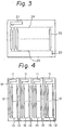
- Figure 3 shows the constitution of a device having a capacity of four mega-bits similar to the device in Fig. 2.
- This device comprises a detector 21, minor loops 22, a generator 23, a read-out major line 24, and a write-in major line 25.
- the device has approximately 2400 minor loops, and each minor loop can store data of approximately 2000 bits.
- Figure 4 shows the constitution of a device consisting of four blocks, each of which is a device of one mega-bit. Each block is the same as the device in Fig. 2.
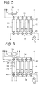
- Figures 5 and 6 show the constitutions of conventional magnetic bubble memory devices, explaining the data storage of the faulty loops.
- the device shown in Fig. 5 uses a marker loop method or a boot-page method.
- the device shown in Fig. 6 uses a boot-loop method. Both devices comprise minor loops (No.1 - No. 4) 41, a write-in major line 33, a read-out major line 34, a detector (D) 39, replicators (R) 42, swap gates (S) 43, a generator (G) 40, and conductors (broken line).
- Only the device shown in Fig. 5 comprises a marker loop 31, and only the device shown in Fig. 6 comprises a boot loop 32, a boot replicator (BR) 44, and a boot swap gate (BS) 45.
- the devices have five minor loops, respectively, as a matter of convenience, although they actually include more than several hundred such loops.
- the device shown in Fig. 5 using the marker loop method uses one of a plurality of minor loops, for example, that nearest to the detector 39, as a marker loop 31. Only one bubble 36 is written-in to the marker loop 31 as a marker. At the bit positions corresponding to the marker bit position in the minor loops No.1 - No. 4, when the minor loop is fault-free, data "1" is written, and when the minor loop is faulty, data "0" is written. As it is assumed in the figure that the minor loop No. 3 is a faulty loop, a bubble is not written at the bit position corresponding to the marker bit position in the minor loop No. 3. The corresponding bit positions in each minor loop are called a page.
- a power source is applied to the device, a controller (not shown) generates a rotating magnetic field for driving, bubbles in the marker loop 31 and the minor loops 41 are moved and, at the same time, replicator pulses are generated continuously at a predetermined time interval, and the marker bubble is detected.
- the number of bits between the outlet of the marker loop 31 and the detector 39 is N bits
- the bubble detected at the Nth period after the replicator pulse is generated is the marker.
- Data series of one page continuing to the marker is faulty loop data. In this operation, at worst, the marker is not detected until all the pages in the marker loop are read.
- the effective access time is increased. For example, when one minor loop has a capacity of 2000 bits, the 1 mega-bit device has 600 minor loops, and the drive signal is 100 kHz, the required time for detecting the marker is at most 12 seconds.
- the device has a boot loop 32 independent of the minor loops No.1 - No. 4.
- This boot loop 32 is connected to the major lines 33 and 34 through the boot swap gate 45 and the boot replicator 44, respectively, and the swap gate 45 and replicator 44 have conductors independent of the other minor loops. This makes possible the exclusive access to the boot loop 32.
- the special data known as header data 37 is written-in. Following the write-in of the header data 37, the faulty loop data 38 is stored.
- the controlle.r when the power source is applied, the controlle.r generates the rotating magnetic field for driving and, at the same time, operates the boot replicator 44 continuously, and the data in the boot loop 32 is read out.
- the controller searches for the header data 37, and the data following the header data 37 is obtained as faulty loop data 38.
- the effective access time is considerably reduced, when compared with the above-mentioned marker loop method.
- the boot loop method is effective in the device having a capacity of only 1 mega-bit, however, where a high density device has a capacity of more than 4 mega-bits, this method has a remarkable defect. Namely, as shown in Fig. 3, since the 4 mega-bits device must perform a high density memory while maintaining the performance of the 1 mega-bit device, the same stored number of bits in one loop in the 4 mega-bits device is selected as for that of the 1 mega-bit device, and the number of the minor loops is four times larger. Therefore, the 4 mega-bits device includes 2400 minor loops, each having a storage capacity of 2000 bits. This means that the faulty loop data cannot be stored in one boot loop.
- the 4 mega-bits device consists of four 1 mega-bit devices and also has four boot loops.
- Figure 7 is a plan view of a magnetic bubble memory device showing the portions of minor loops and gates.
- the reference numerals 71, 72, 73, 74, and 75 are a write-in major line, a swap gate, a replicate gate, a read-out major line, and a soft magnetic pattern, respectively.
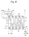
- Figures 8 and 9 show the constitution of a magnetic bubble memory device according to a first embodiment of the present invention, explaining the storage of faulty loop data.
- the device comprises minor loops (No. 1 - No. 4) 61, a boot loop 50, a write-in major line 51, a read-out major line 52, a detector (D) 59, replicators (R) 62, swap gates (S) 63, a boot replicator (BR) 64, a boot swap gate (BS) 65, a generator (G) 60, and conductors (shown by broken lines).
- Header data 53 is stored in the boot loop 50 and faulty loop data 54 is stored in the minor loops 61.
- the faulty loop data 54 is stored at a page n1 bits apart from the page of the last bit of the header data 53.
- the magnetic bubbles are transferred the distance of n1 bits (number of bits) during an n1 times drive period.
- a controller (not shown) generates a rotating magnetic field, continuously operates the boot replicator 64, and searches the header data 53.
- the page in which the faulty loop data is stored is positioned just before the replicator 62, as shown in Fig. 9. Consequently, when the controller generates the replicator pulse, the faulty loop data 54 is reproduced through the replicator 62, and the reproduced bubbles are then transferred on the read-out major line 52. After an (n1 + n2) times drive period from this time, the bubble data detected from the detector 59 is the faulty loop data.
- the storage of the header data 53 can be processed with only one boot loop.
- the time required for detecting the header data 53 is the same as for a conventional device using the boot loop method, therefore, at most, the detection time is 20 mS.
- the time needed until the controller obtains all the faulty loop data becomes longer than for the conventional device using a boot loop method, by 10 uS x (n1 + n2), where 10 pS is a drive period.
- the values n1 and n2 are approximately 100 and 2, respectively, therefore, the excess time is about 1 mS, which is negligible.
- Fig. 10 the above-mentioned time relationship between the detection signal for the header data and the detection signal for the faulty loop data is shown.
- the description (n1 + n2) in the figure signifies that this interval is (drive period) x (n1 + n2).
- Figure 11 shows a constitution of a magnetic bubble memory device according to a second embodiment of the present invention.
- the same elements as in Fig. 8 are referred to by the same reference numerals.
- the device of the second embodiment is different from the first embodiment, in that a plurality of headers 53 and addresses 56-1 and 56-2 to distinguish the headers are written in the boot loop 50. Similar to the first embodiment, the faulty loop data 54-1 (corresponding to the address 56-1) and 54-2 (corresponding to the address 56-2) is written in at a page apart by the predetermined number of bits (or distance) from each header 53.
- the boot replicator 64 is operated continuously and the header data 53 is searched.
- the plurality of headers 53 are memorized, (in the example shown in the figure, two headers 53 are memorized)
- the addresses 56-1 and 56-2 following the header data 53 designate which of the headers is detected.
- the effective access time for obtaining the faulty loop data is at longest one tenth of the access time of the conventional device, namely about 2 mS. This results in a considerable reduction of the access time.
- Figure 12 shows a time relationship among a header detection signal, an address detection signal, and a faulty loop data detection signal which are detected by the detector 59.
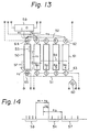
- Figure 13 shows a constitution of a magnetic bubble memory device according to a third embodiment of the present invention.
- the same elements as in Fig. 8 are referred to by the same reference numerals.
- the header data 53 is stored in the boot loop 50 and the faulty loop data 54 is stored at a page apart from the header 53 by the predetermined number of bits.
- an error correction code (ECC) 57 is stored in the boot loop 50 following at a position apart by another predetermined number of bits (n3) from the page in which the faulty loop data are stored.
- the ECC 57 is used to detect the error and error correction.
- the ECC is obtained as a excess value gained by dividing the binary coded faulty loop data by a specific binary function determined by the kind of code.
- the ECC used in this device can be any code, as long as it can be used to correct the error of the faulty loop data.
- the controller searches the header data 53. As soon as the header data 53, is detected the replicator pulse is applied to the replicator 62. After the predetermined number of bits the faulty loop data 54 is detected. Up to this point, the processes are the same as for the first embodiment. Additional in this embodiment, the replicator pulse is generated. After an n3 drive period, the boot replicator 64 is again operated continuously. The number of bits n3 is set so that the detector 59 detects the ECC 57 in series just after the last of the faulty loop data 54.
- a time relationship among a header detection signal, a faulty loop data detection signal, and the ECC detection signal is shown.
- the error of the faulty loop data can be corrected by the ECC.
- the ECC is at most less than 30 bits, and if the plurality of headers as shown in Fig. 11 and a plurality of ECC are stored in the boot loop, the boot loop cannot overflow.
- the present invention applies to a single magnetic bubble memory device, however, this invention can be applied to a magnetic bubble memory device assembly (e.g., Fig. 4) which comprises a plurality of magnetic bubble memory devices.
- a magnetic bubble memory device assembly e.g., Fig. 4
- the header data and the like is stored in a boot loop of at least one of the devices, and the other devices are controlled synchronously by a controller identical to that of the device having the boot loop.
- the faulty loop data stored in the minor loops of each device is processed, in the same way as in a single device.
- the advantages of this invention are applicable in the assembly, as for the single device. As mentioned above, the capacity of the device according to the present invention can be extended over a wide range.
Landscapes
- Engineering & Computer Science (AREA)
- Theoretical Computer Science (AREA)
- Quality & Reliability (AREA)
- Physics & Mathematics (AREA)
- General Engineering & Computer Science (AREA)
- General Physics & Mathematics (AREA)
- Techniques For Improving Reliability Of Storages (AREA)
Description
- The present invention relates to a magnetic bubble memory device, more particularly, to a magnetic bubble memory device wherein the storage arrangement of data for faulty minor loops is improved.
- A magnetic bubble memory device is a solid state memory device having many advantages, for example, non-volatility, easy rewriting, high reliability through the absence of mechanical moving portions, high resistance to environmental changes, high-speed access, and the like. These advantages, together with a tendency to be little affected by vibration and shock, have led to the use of this device as a small file memory in a terminal apparatus. Currently, such a device having a memory capacity of one mega-bit is under mass-production and, in the near future, a device having a memory capacity of four mega-bits will be commercially produced.
- An object of the present invention is to provide a magnetic bubble memory device applicable to a device of more than 4 mega-bits, having a high production yield, and a high-speed detection time for the detection of faulty loop data.
- JP-A-58/41482 describes a magnetic bubble memory device comprising a major line, a bubble detector, minor loops for data storage, and at least one boot loop for storing at least one item of header data to designate a predetermined page and hence a predetermined minor loop of the stored data to enable reading control of data memorized in magnetic bubble form in the minor loops to be performed independently of one another; the magnetic bubble memory also storing data indicating a faulty minor loop. In this arrangement the boot loop stores the faulty loop data and to obtain the header and faulty loop data from the boot loop the memory device must be stepped through a number of steps corresponding to the string of header data and faulty loop data stored in the boot loop.
- According to this invention such a magnetic bubble memory device is characterised in that the faulty loop data is stored in the minor loops at a position a predetermined number of bits apart from a page position in the boot loop in which the last header data corresponding to that minor loop is stored, the predetermined number corresponding to the distance on the major line between the boot loop and the detector so that just after the header data stored in the boot loop is read out, the faulty loop data is transferred out to the major line from the minor loop.
- Preferably the device includes a plurality of major lines, a plurality of bubble detectors and a plurality of groups of minor loops.
- In order that the invention may be better understood, known forms of magnetic bubble memory device will now be described with reference to Figures 1 to 7 and the embodiments of the invention will be described with reference to . Figures 8-13. In the drawings:-
- Figure 1 is an exploded perspective view of a magnetic bubble memory device illustrating the background of the present invention;
- Figures 2, 3 and 4 show constitutions of magnetic bubble memory devices as the background of the present invention;
- Figure 5 explains the storage of faulty loop data in a conventional magnetic bubble memory device using a boot-page method;
- Figure 6 explains the storage of faulty loop data in a conventional magnetic bubble memory device using a boot loop method;
- Figure 7 is a plan view of a chip of a magnetic bubble memory device explaining the background of the present invention;
- Figures 8 and 9 explain the storage of faulty loop data in a magnetic bubble memory device according to a first embodiment of the present invention;
- Figure 10 explains the time relationship between a header detection signal and a detection signal for faulty loop data in the device shown in Figure 8;
- Figure 11 explains the storage of faulty loop data in a magnetic bubble memory device according to a second embodiment of the present invention;
- Figure 12 explains the time relationship between a header detection signal and a detection signal for faulty loop data in the device shown in Figure 11;
- Figure 13 explains the storage of faulty loop data in a magnetic bubble memory device according to a third embodiment of the present invention; and
- Figure 14 explains the time relationship among a header detection signal, a detection signal for faulty loop data, and an error-correction code detection signal.
- To enable the advantages of the present invention to be more fully appreciated, it is necessary to first give a detailed description of the state of the prior art, with reference to the drawings.
- Figure 1 shows the constitution of a magnetic bubble memory device. This device comprises a magnetic
bubble memory chip 1,coils 2 for generating a rotary magnetic field,permanent magnets 3 of bias magnetic field, ashield case 4, and the like. - Usually, a magnetic bubble memory device comprises major/minor loops having major lines and a plurality of minor loops, in which data are stored. Devices having a major/minor loop constitution have a problem, in that faulty minor loops due to crystal defects or to pattern defects occur at a certain rate. The inclusion of a faulty minor loop at less than a predetermined rate is generally allowable. Data relating to the faulty minor loop is usually stored in the bubble memory device and read out by request when the power is switched on. A controller for the magnetic bubble memory device controls the device in accordance with the faulty loop data, to prevent write-in of data in the faulty loops.
- Figure 2 shows the constitution of a device having a capacity of one mega-bit. The device comprises a
detector 11,minor loops 12, agenerator 13, a read-outmajor line 14, and a write-inmajor line 15. The device has approximately 600 minor loops and each minor loop can store data of approximately 2000 bits. - Figure 3 shows the constitution of a device having a capacity of four mega-bits similar to the device in Fig. 2. This device comprises a
detector 21,minor loops 22, agenerator 23, a read-outmajor line 24, and a write-inmajor line 25. The device has approximately 2400 minor loops, and each minor loop can store data of approximately 2000 bits. - Figure 4 shows the constitution of a device consisting of four blocks, each of which is a device of one mega-bit. Each block is the same as the device in Fig. 2.
- Figures 5 and 6 show the constitutions of conventional magnetic bubble memory devices, explaining the data storage of the faulty loops. The device shown in Fig. 5 uses a marker loop method or a boot-page method. The device shown in Fig. 6 uses a boot-loop method. Both devices comprise minor loops (No.1 - No. 4) 41, a write-in
major line 33, a read-outmajor line 34, a detector (D) 39, replicators (R) 42, swap gates (S) 43, a generator (G) 40, and conductors (broken line). Only the device shown in Fig. 5 comprises amarker loop 31, and only the device shown in Fig. 6 comprises aboot loop 32, a boot replicator (BR) 44, and a boot swap gate (BS) 45. In the above description the devices have five minor loops, respectively, as a matter of convenience, although they actually include more than several hundred such loops. - The device shown in Fig. 5 using the marker loop method, uses one of a plurality of minor loops, for example, that nearest to the
detector 39, as amarker loop 31. Only onebubble 36 is written-in to themarker loop 31 as a marker. At the bit positions corresponding to the marker bit position in the minor loops No.1 - No. 4, when the minor loop is fault-free, data "1" is written, and when the minor loop is faulty, data "0" is written. As it is assumed in the figure that the minor loop No. 3 is a faulty loop, a bubble is not written at the bit position corresponding to the marker bit position in the minor loop No. 3. The corresponding bit positions in each minor loop are called a page. - After the above-mentioned storage of faulty loop data has been made, a power source is applied to the device, a controller (not shown) generates a rotating magnetic field for driving, bubbles in the
marker loop 31 and theminor loops 41 are moved and, at the same time, replicator pulses are generated continuously at a predetermined time interval, and the marker bubble is detected. Assuming that the number of bits between the outlet of themarker loop 31 and thedetector 39 is N bits, the bubble detected at the Nth period after the replicator pulse is generated is the marker. Data series of one page continuing to the marker is faulty loop data. In this operation, at worst, the marker is not detected until all the pages in the marker loop are read. Thus the effective access time is increased. For example, when one minor loop has a capacity of 2000 bits, the 1 mega-bit device has 600 minor loops, and the drive signal is 100 kHz, the required time for detecting the marker is at most 12 seconds. - In the device shown in Fig. 6 using the boot loop method, the device has a
boot loop 32 independent of the minor loops No.1 - No. 4. Thisboot loop 32 is connected to themajor lines boot swap gate 45 and theboot replicator 44, respectively, and theswap gate 45 andreplicator 44 have conductors independent of the other minor loops. This makes possible the exclusive access to theboot loop 32. In theboot loop 32 of the device, the special data known asheader data 37 is written-in. Following the write-in of theheader data 37, thefaulty loop data 38 is stored. In this state, when the power source is applied, the controlle.r generates the rotating magnetic field for driving and, at the same time, operates theboot replicator 44 continuously, and the data in theboot loop 32 is read out. The controller searches for theheader data 37, and the data following theheader data 37 is obtained asfaulty loop data 38. In this case, assuming that one loop includes 2000 bits and the 1 mega-bit device having 600 minor loops is operated by the drive signal of 100 kHz, the longest time needed for detecting the header is 2000 x 10 ps = 20 mS. Thus the effective access time is considerably reduced, when compared with the above-mentioned marker loop method. - The boot loop method is effective in the device having a capacity of only 1 mega-bit, however, where a high density device has a capacity of more than 4 mega-bits, this method has a remarkable defect. Namely, as shown in Fig. 3, since the 4 mega-bits device must perform a high density memory while maintaining the performance of the 1 mega-bit device, the same stored number of bits in one loop in the 4 mega-bits device is selected as for that of the 1 mega-bit device, and the number of the minor loops is four times larger. Therefore, the 4 mega-bits device includes 2400 minor loops, each having a storage capacity of 2000 bits. This means that the faulty loop data cannot be stored in one boot loop.
- In an attempt to avoid this defect, the idea shown in Fig. 4 has been tried, in which the 4 mega-bits device consists of four 1 mega-bit devices and also has four boot loops. In this device, the four boot loops must be fault-free, and faulty loops are included at a certain probability ratio. Therefore, in these boot loops, faulty loops are produced at the same probability. That is, assuming that in a 1 mega-bit device one chip in ten has a faulty boot loop, the probability of all four boot loops being fault-free is (9/10)'* = 0.66. As can be understood from this calculation, approximately one-third of the chips become defective and cannot be used for a magnetic bubble memory device. This is a considerable defect.
- Figure 7 is a plan view of a magnetic bubble memory device showing the portions of minor loops and gates. In the figure the
reference numerals - Now, embodiments of the present invention will be explained, with reference to the drawings.
- Figures 8 and 9 show the constitution of a magnetic bubble memory device according to a first embodiment of the present invention, explaining the storage of faulty loop data. In the drawings, the device comprises minor loops (No. 1 - No. 4) 61, a
boot loop 50, a write-inmajor line 51, a read-outmajor line 52, a detector (D) 59, replicators (R) 62, swap gates (S) 63, a boot replicator (BR) 64, a boot swap gate (BS) 65, a generator (G) 60, and conductors (shown by broken lines).Header data 53 is stored in theboot loop 50 andfaulty loop data 54 is stored in theminor loops 61. - In this embodiment, if the distance between the
boot replicator 64 and thedetector 59 is n1 bits, and the distance between theboot replicator 64 and the minor loop No. 1 is n2 bits, thefaulty loop data 54 is stored at a page n1 bits apart from the page of the last bit of theheader data 53. The magnetic bubbles are transferred the distance of n1 bits (number of bits) during an n1 times drive period. - In this state, when the power source is supplied, a controller (not shown) generates a rotating magnetic field, continuously operates the
boot replicator 64, and searches theheader data 53. When the last bit of theheader data 53 passes through thedetector 59, namely, when theheader data 53 has been detected, the page in which the faulty loop data is stored is positioned just before thereplicator 62, as shown in Fig. 9. Consequently, when the controller generates the replicator pulse, thefaulty loop data 54 is reproduced through thereplicator 62, and the reproduced bubbles are then transferred on the read-outmajor line 52. After an (n1 + n2) times drive period from this time, the bubble data detected from thedetector 59 is the faulty loop data. - According to this embodiment, since only the
header data 53 is stored in theboot loop 50, even when applying a device having more minor loops than there are bit numbers of the boot loop, wherein, in the conventional boot loop method, faulty loop data storage cannot be performed, the storage of theheader data 53 can be processed with only one boot loop. - The time required for detecting the
header data 53 is the same as for a conventional device using the boot loop method, therefore, at most, the detection time is 20 mS. The time needed until the controller obtains all the faulty loop data becomes longer than for the conventional device using a boot loop method, by 10 uS x (n1 + n2), where 10 pS is a drive period. However, the values n1 and n2 are approximately 100 and 2, respectively, therefore, the excess time is about 1 mS, which is negligible. - In Fig. 10, the above-mentioned time relationship between the detection signal for the header data and the detection signal for the faulty loop data is shown. The description (n1 + n2) in the figure signifies that this interval is (drive period) x (n1 + n2).
- Figure 11 shows a constitution of a magnetic bubble memory device according to a second embodiment of the present invention. In the figure, the same elements as in Fig. 8 are referred to by the same reference numerals.
- The device of the second embodiment is different from the first embodiment, in that a plurality of
headers 53 and addresses 56-1 and 56-2 to distinguish the headers are written in theboot loop 50. Similar to the first embodiment, the faulty loop data 54-1 (corresponding to the address 56-1) and 54-2 (corresponding to the address 56-2) is written in at a page apart by the predetermined number of bits (or distance) from eachheader 53. When the power source is switched on, similar to the first embodiment, theboot replicator 64 is operated continuously and theheader data 53 is searched. In this case, since the plurality ofheaders 53 are memorized, (in the example shown in the figure, twoheaders 53 are memorized), compared with the device having only one header, only half the time, at longest, is required to detect theheader data 53. The addresses 56-1 and 56-2 following theheader data 53 designate which of the headers is detected. - In the device of the second embodiment, only the headers and the addresses are stored. The sum of the bit of a header and an address is at most several ten bits, therefore, more than ten headers can be stored in the boot loop having a capacity of 2000 bits. In the case of storing ten headers, the effective access time for obtaining the faulty loop data is at longest one tenth of the access time of the conventional device, namely about 2 mS. This results in a considerable reduction of the access time.
- Figure 12 shows a time relationship among a header detection signal, an address detection signal, and a faulty loop data detection signal which are detected by the
detector 59. - Figure 13 shows a constitution of a magnetic bubble memory device according to a third embodiment of the present invention. In the figure, the same elements as in Fig. 8 are referred to by the same reference numerals.
- In the device of the third embodiment, similar to the first embodiment, the
header data 53 is stored in theboot loop 50 and thefaulty loop data 54 is stored at a page apart from theheader 53 by the predetermined number of bits. However, different from the first embodiment, an error correction code (ECC) 57 is stored in theboot loop 50 following at a position apart by another predetermined number of bits (n3) from the page in which the faulty loop data are stored. - The
ECC 57 is used to detect the error and error correction. For example, the ECC is obtained as a excess value gained by dividing the binary coded faulty loop data by a specific binary function determined by the kind of code. The ECC used in this device can be any code, as long as it can be used to correct the error of the faulty loop data. - When the power source is switched on, the controller searches the
header data 53. As soon as theheader data 53, is detected the replicator pulse is applied to thereplicator 62. After the predetermined number of bits thefaulty loop data 54 is detected. Up to this point, the processes are the same as for the first embodiment. Additional in this embodiment, the replicator pulse is generated. After an n3 drive period, theboot replicator 64 is again operated continuously. The number of bits n3 is set so that thedetector 59 detects theECC 57 in series just after the last of thefaulty loop data 54. - In Fig. 14, a time relationship among a header detection signal, a faulty loop data detection signal, and the ECC detection signal is shown.
- Using the device of this embodiment, the error of the faulty loop data can be corrected by the ECC. Thus, the reliability of the device can be considerably increased. The ECC is at most less than 30 bits, and if the plurality of headers as shown in Fig. 11 and a plurality of ECC are stored in the boot loop, the boot loop cannot overflow.
- In the above-mentioned embodiments, the present invention applies to a single magnetic bubble memory device, however, this invention can be applied to a magnetic bubble memory device assembly (e.g., Fig. 4) which comprises a plurality of magnetic bubble memory devices. In this case, the header data and the like is stored in a boot loop of at least one of the devices, and the other devices are controlled synchronously by a controller identical to that of the device having the boot loop. In this way, in the assembly, the faulty loop data stored in the minor loops of each device is processed, in the same way as in a single device. The advantages of this invention are applicable in the assembly, as for the single device. As mentioned above, the capacity of the device according to the present invention can be extended over a wide range.
Claims (4)
characterized in that the faulty loop data is stored in the minor loops (61) at a position a predetermined number (n1) of bits apart from a page position in the boot loop (50) in which the last header data corresponding to that minor loop
Applications Claiming Priority (2)
| Application Number | Priority Date | Filing Date | Title |
|---|---|---|---|
| JP58094961A JPS59221886A (en) | 1983-05-31 | 1983-05-31 | Defective loop information storing system of magnetic bubble memory element |
| JP94961/83 | 1983-05-31 |
Publications (3)
| Publication Number | Publication Date |
|---|---|
| EP0127350A2 EP0127350A2 (en) | 1984-12-05 |
| EP0127350A3 EP0127350A3 (en) | 1987-03-04 |
| EP0127350B1 true EP0127350B1 (en) | 1990-01-31 |
Family
ID=14124524
Family Applications (1)
| Application Number | Title | Priority Date | Filing Date |
|---|---|---|---|
| EP84303045A Expired EP0127350B1 (en) | 1983-05-31 | 1984-05-04 | Magnetic bubble memory device |
Country Status (5)
| Country | Link |
|---|---|
| US (1) | US4590587A (en) |
| EP (1) | EP0127350B1 (en) |
| JP (1) | JPS59221886A (en) |
| CA (1) | CA1217860A (en) |
| DE (1) | DE3481243D1 (en) |
Family Cites Families (7)
| Publication number | Priority date | Publication date | Assignee | Title |
|---|---|---|---|---|
| US4159412A (en) * | 1977-02-11 | 1979-06-26 | Texas Instruments Incorporated | Magnetic bubble memory chip synchronization and redundancy |
| US4090251A (en) * | 1977-06-09 | 1978-05-16 | Texas Instruments Incorporated | Bubble memory redundancy storage |
| JPS5925307B2 (en) * | 1978-02-17 | 1984-06-16 | 株式会社日立製作所 | Storage device |
| JPS5613580A (en) * | 1979-07-13 | 1981-02-09 | Nec Corp | Magnetic bubble memory unit |
| JPS57113478A (en) * | 1980-12-29 | 1982-07-14 | Fujitsu Ltd | Magnetic bubble memory controlling system |
| JPS5841482A (en) * | 1981-09-03 | 1983-03-10 | Nec Corp | Magnetic bubble memory chip |
| JPS58141493A (en) * | 1982-02-16 | 1983-08-22 | Nec Corp | Magnetic bubble storage element |
-
1983
- 1983-05-31 JP JP58094961A patent/JPS59221886A/en active Granted
-
1984
- 1984-05-01 CA CA000453251A patent/CA1217860A/en not_active Expired
- 1984-05-02 US US06/606,407 patent/US4590587A/en not_active Expired - Fee Related
- 1984-05-04 DE DE8484303045T patent/DE3481243D1/en not_active Expired - Fee Related
- 1984-05-04 EP EP84303045A patent/EP0127350B1/en not_active Expired
Also Published As
| Publication number | Publication date |
|---|---|
| JPS623510B2 (en) | 1987-01-26 |
| JPS59221886A (en) | 1984-12-13 |
| CA1217860A (en) | 1987-02-10 |
| US4590587A (en) | 1986-05-20 |
| DE3481243D1 (en) | 1990-03-08 |
| EP0127350A2 (en) | 1984-12-05 |
| EP0127350A3 (en) | 1987-03-04 |
Similar Documents
| Publication | Publication Date | Title |
|---|---|---|
| EP0274817B1 (en) | Data storage system | |
| US5438573A (en) | Flash EEPROM array data and header file structure | |
| KR960001948B1 (en) | Method and apparatus for programmable memory control with | |
| EP0185924A3 (en) | Buffer system with detection of read or write circuits' failures | |
| US5490264A (en) | Generally-diagonal mapping of address space for row/column organizer memories | |
| US4878220A (en) | Semiconductor memory device | |
| US5432802A (en) | Information processing device having electrically erasable programmable read only memory with error check and correction circuit | |
| US4891811A (en) | Efficient address test for large memories | |
| US4926426A (en) | Error correction check during write cycles | |
| JPS6042560B2 (en) | semiconductor storage device | |
| EP0090219B1 (en) | Memory system restructured by deterministic permutation algorithm | |
| EP0614193A2 (en) | Method and apparatus for detecting retention faults in memories | |
| US4354253A (en) | Bubble redundancy map storage using non-volatile semiconductor memory | |
| US4027283A (en) | Resynchronizable bubble memory | |
| US4073012A (en) | Fault-tolerant memory organization | |
| US4453248A (en) | Fault alignment exclusion method to prevent realignment of previously paired memory defects | |
| CN107025937B (en) | Reading method of memory and memory device | |
| EP0127350B1 (en) | Magnetic bubble memory device | |
| US5392294A (en) | Diagnostic tool and method for locating the origin of parasitic bit faults in a memory array | |
| EP1001432A1 (en) | Method of testing random-access memory | |
| EP0011717B1 (en) | A magnetic bubble domain memory system | |
| US4592016A (en) | Magnetic bubble memory device | |
| JPS6161288A (en) | Magnetic bubble memory | |
| EP0115144A2 (en) | Method of testing bubble memory devices | |
| US4139886A (en) | Fault tolerant system for bubble memories |
Legal Events
| Date | Code | Title | Description |
|---|---|---|---|
| PUAI | Public reference made under article 153(3) epc to a published international application that has entered the european phase |
Free format text: ORIGINAL CODE: 0009012 |
|
| AK | Designated contracting states |
Designated state(s): DE FR GB NL |
|
| PUAL | Search report despatched |
Free format text: ORIGINAL CODE: 0009013 |
|
| AK | Designated contracting states |
Kind code of ref document: A3 Designated state(s): DE FR GB NL |
|
| 17P | Request for examination filed |
Effective date: 19870821 |
|
| 17Q | First examination report despatched |
Effective date: 19880708 |
|
| GRAA | (expected) grant |
Free format text: ORIGINAL CODE: 0009210 |
|
| AK | Designated contracting states |
Kind code of ref document: B1 Designated state(s): DE FR GB NL |
|
| ET | Fr: translation filed | ||
| REF | Corresponds to: |
Ref document number: 3481243 Country of ref document: DE Date of ref document: 19900308 |
|
| PLBE | No opposition filed within time limit |
Free format text: ORIGINAL CODE: 0009261 |
|
| STAA | Information on the status of an ep patent application or granted ep patent |
Free format text: STATUS: NO OPPOSITION FILED WITHIN TIME LIMIT |
|
| 26N | No opposition filed | ||
| PGFP | Annual fee paid to national office [announced via postgrant information from national office to epo] |
Ref country code: GB Payment date: 19920424 Year of fee payment: 9 |
|
| PGFP | Annual fee paid to national office [announced via postgrant information from national office to epo] |
Ref country code: FR Payment date: 19920527 Year of fee payment: 9 |
|
| PGFP | Annual fee paid to national office [announced via postgrant information from national office to epo] |
Ref country code: NL Payment date: 19920531 Year of fee payment: 9 |
|
| PGFP | Annual fee paid to national office [announced via postgrant information from national office to epo] |
Ref country code: DE Payment date: 19920727 Year of fee payment: 9 |
|
| PG25 | Lapsed in a contracting state [announced via postgrant information from national office to epo] |
Ref country code: GB Effective date: 19930504 |
|
| PG25 | Lapsed in a contracting state [announced via postgrant information from national office to epo] |
Ref country code: NL Effective date: 19931201 |
|
| GBPC | Gb: european patent ceased through non-payment of renewal fee |
Effective date: 19930504 |
|
| NLV4 | Nl: lapsed or anulled due to non-payment of the annual fee | ||
| PG25 | Lapsed in a contracting state [announced via postgrant information from national office to epo] |
Ref country code: FR Effective date: 19940131 |
|
| PG25 | Lapsed in a contracting state [announced via postgrant information from national office to epo] |
Ref country code: DE Effective date: 19940201 |
|
| REG | Reference to a national code |
Ref country code: FR Ref legal event code: ST |