EP0125805A2 - Bit-Fehler Detektionsschaltung für eine PSK-modulierte Trägerwelle - Google Patents
Bit-Fehler Detektionsschaltung für eine PSK-modulierte Trägerwelle Download PDFInfo
- Publication number
- EP0125805A2 EP0125805A2 EP84302609A EP84302609A EP0125805A2 EP 0125805 A2 EP0125805 A2 EP 0125805A2 EP 84302609 A EP84302609 A EP 84302609A EP 84302609 A EP84302609 A EP 84302609A EP 0125805 A2 EP0125805 A2 EP 0125805A2
- Authority
- EP
- European Patent Office
- Prior art keywords
- carrier wave
- signal
- phase
- output
- circuit
- Prior art date
- Legal status (The legal status is an assumption and is not a legal conclusion. Google has not performed a legal analysis and makes no representation as to the accuracy of the status listed.)
- Granted
Links
- 238000001514 detection method Methods 0.000 title claims abstract description 21
- 238000011084 recovery Methods 0.000 claims abstract description 21
- 230000005540 biological transmission Effects 0.000 description 10
- 238000010586 diagram Methods 0.000 description 9
- 238000004891 communication Methods 0.000 description 7
- 238000010276 construction Methods 0.000 description 2
- 238000001228 spectrum Methods 0.000 description 2
- 238000000411 transmission spectrum Methods 0.000 description 2
- 238000006243 chemical reaction Methods 0.000 description 1
- 230000006866 deterioration Effects 0.000 description 1
- 238000000034 method Methods 0.000 description 1
- 238000012544 monitoring process Methods 0.000 description 1
- 230000010363 phase shift Effects 0.000 description 1
- 238000005070 sampling Methods 0.000 description 1
- 238000007493 shaping process Methods 0.000 description 1
- 230000001360 synchronised effect Effects 0.000 description 1
Images


Classifications
-
- H—ELECTRICITY
- H04—ELECTRIC COMMUNICATION TECHNIQUE
- H04L—TRANSMISSION OF DIGITAL INFORMATION, e.g. TELEGRAPHIC COMMUNICATION
- H04L27/00—Modulated-carrier systems
- H04L27/18—Phase-modulated carrier systems, i.e. using phase-shift keying
- H04L27/22—Demodulator circuits; Receiver circuits
- H04L27/227—Demodulator circuits; Receiver circuits using coherent demodulation
- H04L27/2275—Demodulator circuits; Receiver circuits using coherent demodulation wherein the carrier recovery circuit uses the received modulated signals
-
- H—ELECTRICITY
- H04—ELECTRIC COMMUNICATION TECHNIQUE
- H04L—TRANSMISSION OF DIGITAL INFORMATION, e.g. TELEGRAPHIC COMMUNICATION
- H04L1/00—Arrangements for detecting or preventing errors in the information received
- H04L1/24—Testing correct operation
- H04L1/241—Testing correct operation using pseudo-errors
Definitions
- the present invention relates to a bit error detection circuit for use in a digital communication system such as TD MA (Time Division Multiplex Access)communication system, which checks the quality of a transmission line.
- TD MA Time Division Multiplex Access
- bit error rate BER
- directly determining a BER from a received signal is in many cases impossible because transmitted data is unknown. More accepted, therefore, is a method which predicts a BER of a received signal from information provided by comparing a main reproduced signal with a signal having a falsely deteriorated characteristic.
- a prior art bit error detection circuit of the type described comprises, for example, first and second discriminator circuits adapted to discriminate an output of a phase demodulator with respect to first and second different reference voltages respectively, and a circuit for measuring a false BER by comparing an output of the second discriminator circuit with an output of the second discriminator circuit.
- a problem encountered with such a circuit construction is that in the TDMA communication of a burst PSK (phase Shift Keying) modulated carrier wave for example, the burst carrier wave level and, therefore, the predicted BER differs from one station to another.
- PSK phase Shift Keying
- Another prior art bit error detection circuit comprises first and second discriminator circuits adapted to discriminate the output of a phase demodulator at a time corresponding to the center ⁇ 0 of data (bit) and a time deviated by a phase ⁇ 1 from the center e 0 respectively, and a circuit for measuring a pseudo BER by comparing the output of the second discriminator circuit with the output of the first discriminator circuit.
- This is not acceptable in the case of a transmission line which includes a high power amplifier or like non-linear element because, as will be described in detail, the operating point of a non-linear element changes depending upon the operation mode, i.e. linear mode or non-linear mode. Such is presumably attributable to a change in the amount of variation in intersymbol interference from the phase point ⁇ 0 to the phase point ⁇ 1 .
- a bit error detection circuit comprising first demodulator means supplied with a reference carrier wave for phase-demodulating an input PSK modulated carrier wave into a first demodulated signal; carrier wave recovery means for providing the reference carrier wave in response to the input PSK modulated carrier wave or the first demodulated signal; clock signal recovery means for providing a clock signal in response to the input PSK modulated carrier wave or the first demodulated signal; oscillator means; modulator means for phase-modulating the reference carrier wave with the output of the oscillator means; second demodulator means supplied with the output of said modulator means for phase-demodulating the input PSK modulated carrier wave into a second demodulated signal; first discriminator means for discriminating the first demodulated signal into a first digital signal in response to the clock signal; second discriminator means for discriminating the second demodulated signal into a second digital signal in response to the clock signal; and comparator means for comparing the first digital signal with the second digital signal to provide a bit error detection signal.
- the bit error detection circuit comprises a modulated carrier wave input terminal 101, a recovered carrier wave input terminal 102, a 2-phase phase demodulator 103, a first discriminator circuit 104, a second discriminator circuit 105, a comparator circuit or an Exclusive-OR circuit 106, a pseudo error output terminal 107, a carrier recovery circuit 108 and a clock signal recovery circuit 109.
- a 2-phase PSK modulated carrier wave coming in through the terminal 101 is applied to the demodulator 103, the carrier wave recovery circuit 108 and the clock signal recovery circuit 109.
- the demodulator 103 demodulates the modulated carrier wave with a recovered carrier wave supplied from the circuit 108 (comprising a frequency multiplier, a filter and a frequency divider, for example).
- the demodulator output has an eye pattern shown in Fig. 2.
- Each of the discriminator 104 and 105 comprises a voltage comparator and a sampler.
- the output of the discriminator 105 is larger in bit error rate than the output of the discriminator 104. Therefore, the psuedo BER of the output of the discriminator 105 can be measured by comparing the output of the discriminator 105 with the output of the discriminator 104 at the comparator 106.
- the received burst signal level differs from one station to another as represented by those of stations A and B in Fig. 3. Because the threshold level assigned to the discriminator 105 is V bolt which is constant, a presumed BER for the station A is different from one for the station B. For this reason, although the prior art circuit of F ig. 1 may solve the above problem by employing an automatic gain control (AGC) circuit at a stage ahead of the demodulator in the case of a continuous signal, it is ineffective for a system in which the received signal level changes between bursts. For details of such a circuit, reference may be made to U.S. Patent 4,188,615 issued February 2, 1980 and assigned to NEC Corporation.
- AGC automatic gain control
- the bit error detection circuit comprises a modulated wave input terminal 201, a recovered carrier wave input terminal 202, a clock signal input terminal 203, a phase demodulator circuit 204, a first discriminator 205, a second discriminator 206, a comparator circuit 207, a phase shifter circuit 208, a pseudo error output terminal 209, a clock signal recovery circuit 210, and a carrier wave recovery circuit 211.
- a PSK modulated carrier wave arriving at the terminal 201 is phase-demodulated with the recovered carrier wave supplied to the phase demodulator 204 as reference.
- the output of the demodulator 204 is supplied to the discriminators 205 and 206.
- a clock signal is supplied to the terminal 203 from the clock signal recovery circuit 210 and is synchonous with the PSK modulated carrier wave.
- the clock signal is applied to the first discriminator 205 which then discriminates the demodulator-output with respect to a phase 9 0 of the center of an eye pattern or the center of each bit shown in Fig. 5.
- the clock signal is also supplied to the phase shifter 208 to be thereby phase-shifted by ⁇ 1 .
- the output of the phase shifter 208 is fed to the discriminator 206 which then discriminates the demodulator output with respect to a phase point ⁇ 1 shown in Fig. 5.
- the result of discrimination at the phase point e 1 involves a greater error than the result of discrimination at the phase point ⁇ 0 .
- the output of the discriminator 206 is compared with the output of the discriminator 205, so that a true BER of the output signal of the discriminator 205 (or the output appearing at the pseudo error output terminal 209).
- Each of the discriminators may comprise a voltage comparator and a sampler, or a flip-flop.
- the clock signal recovery circuit may provide a clock signal in response to the output of the phase demodulator.
- the carrier wave recovery circuit may comprise an error signal generating circuit responsive to the output of the phase demodulator, a lowpass filter responsive to the output of the generating circuit, and a voltage controlled oscillator response to the output of the lowpass filter for providing a carrier wave.
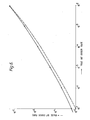
- FIG. 7 A model transmission line with a non-linear element is shown in a block diagram in Fig. 7. There are shown in Fig. 7 a transmitter section 301, a high power amplifier (HPA) 302, a satellite repeater 303 including an amplifier (TWTA), and a receiving filter 304. In this drawing, both the TWTA and HPA comprise non-linear elements. Shown in Fig. 6 is a graph representative of a relationship between a false BER and a true BER in the bit error detection circuit of Fig.
- the circuit comprises an input terminal 401, a carrier wave recovery circuit 403, first and second phase demodulators 405 and 406, a phase modulator 407, an oscillator 408, a comparator circuit 409, an output terminal 410, a clock signal recovery circuit 411, and discriminator circuits 412 and 413 having a common discrimination level.
- the carrier wave recovery circuit 403 comprises a frequency multiplier for multiplying, for example, an N-phase phase modulated carrier wave by "N", a filter for picking up the N-multiplied freauency and a divider for dividing the output of the filter by "N".
- the clock recovery circuit 411 is made up of a delay circuit for delaying a demodulated signal by half a bit, a multiplier for multiplying the demodulator output and the output of the delay circuit, a tuning circuit synchronous to a clock component of the output of the multiplier, and a circuit for wave-shaping the output of the tuning circuit to provide recovered clock pulse. It is also possible to extract the clock signal out of the input modulated carrier ware, as shown in Fig. 1 or 4.
- an input PSK modulated carrier wave coming in through the input terminal 401 is supplied to the phase demodulators 405 and 406 and the carrier recovery circuit 403.
- the recovered carrier wave from the circuit 403 is applied to the phase demodulator 405 in which the PSK modulated carrier wave is phase-demodulated.
- the recovered carrier wave is applied to the phase modulator 407 to be thereby phase-modulated in response to the output signal of the oscillator 408.
- the output of the phase modulator 407 is delivered to the phase demodulator 406 which then phase-demodulates the modulated carrier wave.
- each of the discriminator circuits 412 and 413 discriminates the output of the demodulator associated therewith at the center of the bit.
- the outputs of the circuits 412 and 413 are commonly delivered to the comparator 409 whose output appears at the terminal 410 as a pseudo error signal.
- the signal incoming at the input terminal 401 is a 4-phase PSK modulated carrier wave a (t) sin ⁇ c t + b(t)cos ⁇ c t, and the recovered carrier wave output from the carrier wave recovery circuit 403 is sin ⁇ Then, the first phase demodulator 405 develops output signals a(t) and b(t).
- the second phase demodulator 406 develops an output signal a(t) cos ⁇ (t) - b(t) sin 0(t) and a(t) sin 9 (t) + b (t) cos ⁇ (t)-Outputs of the first and second phase demodulators 405 and 406 are shown in eye patterns in Figs. 9A and 9B.
- the pseudo BER allows a true BER of an output of the demodulator 405 to be predicted. Such comparison effected at the same time instant will cause hardly any deterioration to characteristics even if the operating point of a non-linear element on the transmission line is changed.
- Fig. 10 is a graph showing a relationship between a false BER and a true BER of a PSK modulated carrier wave passed through the transmission line of Fig. 7, attained by calculation with the bit error detector shown in Fig. 8.
- the circuitry in accordance with the present invention is advantageous over the prior art circuitry shown in Fig. 4 in that it is capable of predicting a true BER more correctly despite the change in the operating point of a non-linear element. Furthermore, the prediction is free from the influence of the change in input level because the threshold level is set at the center of an eye pattern.
- the present invention provides a bit error detection circuit which is effective to reduce an error in the prediction of a true BER of a received and reproduced signal relative to a false B E R due to the fluctuation in the level of an input signal or that in the operating point of a non-linear element.
Landscapes
- Engineering & Computer Science (AREA)
- Computer Networks & Wireless Communication (AREA)
- Signal Processing (AREA)
- Digital Transmission Methods That Use Modulated Carrier Waves (AREA)
- Detection And Prevention Of Errors In Transmission (AREA)
- Dc Digital Transmission (AREA)
Applications Claiming Priority (2)
| Application Number | Priority Date | Filing Date | Title |
|---|---|---|---|
| JP58067024A JPS59193658A (ja) | 1983-04-18 | 1983-04-18 | 擬似誤り検出回路 |
| JP67024/83 | 1983-04-18 |
Publications (3)
| Publication Number | Publication Date |
|---|---|
| EP0125805A2 true EP0125805A2 (de) | 1984-11-21 |
| EP0125805A3 EP0125805A3 (en) | 1986-07-30 |
| EP0125805B1 EP0125805B1 (de) | 1989-07-12 |
Family
ID=13332904
Family Applications (1)
| Application Number | Title | Priority Date | Filing Date |
|---|---|---|---|
| EP84302609A Expired EP0125805B1 (de) | 1983-04-18 | 1984-04-17 | Bit-Fehler Detektionsschaltung für eine PSK-modulierte Trägerwelle |
Country Status (5)
| Country | Link |
|---|---|
| US (1) | US4628507A (de) |
| EP (1) | EP0125805B1 (de) |
| JP (1) | JPS59193658A (de) |
| CA (1) | CA1231388A (de) |
| DE (1) | DE3478982D1 (de) |
Families Citing this family (34)
| Publication number | Priority date | Publication date | Assignee | Title |
|---|---|---|---|---|
| US4920537A (en) * | 1988-07-05 | 1990-04-24 | Darling Andrew S | Method and apparatus for non-intrusive bit error rate testing |
| US5036515A (en) * | 1989-05-30 | 1991-07-30 | Motorola, Inc. | Bit error rate detection |
| US4987386A (en) * | 1989-10-03 | 1991-01-22 | Communications Satellite Corporation | Coherent phase and frequency recovery method and circuit |
| US5220581A (en) * | 1991-03-28 | 1993-06-15 | International Business Machines Corporation | Digital data link performance monitor |
| FR2694855B1 (fr) * | 1992-08-14 | 1994-09-30 | Alcatel Espace | Dispositif de commutation transparente, notamment pour le domaine spatial, architectures de charge utile utilisant un tel dispositif, et procédés de mise en Óoeuvre du dispositif et des architectures. |
| US5418789A (en) * | 1992-10-14 | 1995-05-23 | International Business Machines Corporation | Fast communication link bit error rate estimator |
| KR100415993B1 (ko) * | 2000-05-15 | 2004-01-24 | 마쯔시다덴기산교 가부시키가이샤 | 디지털 복조장치 |
| US6650711B1 (en) * | 2000-06-02 | 2003-11-18 | Tropian, Inc. | Quadrature modulation with reduced phase-error distortion |
| US7502430B2 (en) | 2001-04-27 | 2009-03-10 | The Directv Group, Inc. | Coherent averaging for measuring traveling wave tube amplifier nonlinearity |
| US7151807B2 (en) * | 2001-04-27 | 2006-12-19 | The Directv Group, Inc. | Fast acquisition of timing and carrier frequency from received signal |
| US7639759B2 (en) | 2001-04-27 | 2009-12-29 | The Directv Group, Inc. | Carrier to noise ratio estimations from a received signal |
| US7822154B2 (en) | 2001-04-27 | 2010-10-26 | The Directv Group, Inc. | Signal, interference and noise power measurement |
| US7173981B1 (en) | 2001-04-27 | 2007-02-06 | The Directv Group, Inc. | Dual layer signal processing in a layered modulation digital signal system |
| US7209524B2 (en) | 2001-04-27 | 2007-04-24 | The Directv Group, Inc. | Layered modulation for digital signals |
| US7184473B2 (en) | 2001-04-27 | 2007-02-27 | The Directv Group, Inc. | Equalizers for layered modulated and other signals |
| US8005035B2 (en) | 2001-04-27 | 2011-08-23 | The Directv Group, Inc. | Online output multiplexer filter measurement |
| US7423987B2 (en) | 2001-04-27 | 2008-09-09 | The Directv Group, Inc. | Feeder link configurations to support layered modulation for digital signals |
| US7184489B2 (en) | 2001-04-27 | 2007-02-27 | The Directv Group, Inc. | Optimization technique for layered modulation |
| US7583728B2 (en) | 2002-10-25 | 2009-09-01 | The Directv Group, Inc. | Equalizers for layered modulated and other signals |
| US7483505B2 (en) | 2001-04-27 | 2009-01-27 | The Directv Group, Inc. | Unblind equalizer architecture for digital communication systems |
| US7471735B2 (en) | 2001-04-27 | 2008-12-30 | The Directv Group, Inc. | Maximizing power and spectral efficiencies for layered and conventional modulations |
| US7245671B1 (en) | 2001-04-27 | 2007-07-17 | The Directv Group, Inc. | Preprocessing signal layers in a layered modulation digital signal system to use legacy receivers |
| CA2489569C (en) | 2002-07-01 | 2012-05-22 | The Directv Group, Inc. | Improving hierarchical 8psk performance |
| TWI279113B (en) | 2002-07-03 | 2007-04-11 | Hughes Electronics Corp | Method and apparatus for layered modulation |
| US7230480B2 (en) | 2002-10-25 | 2007-06-12 | The Directv Group, Inc. | Estimating the operating point on a non-linear traveling wave tube amplifier |
| US7463676B2 (en) | 2002-10-25 | 2008-12-09 | The Directv Group, Inc. | On-line phase noise measurement for layered modulation |
| US7474710B2 (en) | 2002-10-25 | 2009-01-06 | The Directv Group, Inc. | Amplitude and phase matching for layered modulation reception |
| ES2398213T3 (es) | 2002-10-25 | 2013-03-14 | The Directv Group, Inc. | Procesador de señal de modulación en capas de baja complejidad |
| US7529312B2 (en) | 2002-10-25 | 2009-05-05 | The Directv Group, Inc. | Layered modulation for terrestrial ATSC applications |
| US7173977B2 (en) | 2002-10-25 | 2007-02-06 | The Directv Group, Inc. | Method and apparatus for tailoring carrier power requirements according to availability in layered modulation systems |
| US7502429B2 (en) | 2003-10-10 | 2009-03-10 | The Directv Group, Inc. | Equalization for traveling wave tube amplifier nonlinearity measurements |
| US7298788B2 (en) * | 2003-10-27 | 2007-11-20 | Ge Medical Systems Information Technologies, Inc. | Wireless communication system and method |
| JP6052598B2 (ja) | 2012-01-30 | 2016-12-27 | 株式会社リコー | 定着装置および画像形成装置 |
| DE102013220156B4 (de) * | 2012-10-05 | 2017-03-23 | Infineon Technologies Ag | Testschaltkreis |
Citations (1)
| Publication number | Priority date | Publication date | Assignee | Title |
|---|---|---|---|---|
| GB2072997A (en) * | 1980-03-29 | 1981-10-07 | Licentia Gmbh | Method of determining the bit error rate in a digital signnal transmission |
Family Cites Families (7)
| Publication number | Priority date | Publication date | Assignee | Title |
|---|---|---|---|---|
| IT1041378B (it) * | 1975-06-10 | 1980-01-10 | Cselt Centro Studi Lab Telecom | Dispositivo per il rilevamento della qualita di trasmissione nei ricevitori di segnali numerici |
| FR2390052B1 (de) * | 1977-05-06 | 1981-07-03 | Poitevin Jean Pierre | |
| JPS5431212A (en) * | 1977-08-15 | 1979-03-08 | Nec Corp | Monitor circuit for digital signal transmission line |
| JPS5469311A (en) * | 1977-11-15 | 1979-06-04 | Fujitsu Ltd | Supervisory unit for error ratio of n-phase psk digital modulation system |
| JPS54152802A (en) * | 1978-05-23 | 1979-12-01 | Fujitsu Ltd | Error rate supervisory system |
| US4218771A (en) * | 1978-12-04 | 1980-08-19 | Rockwell International Corporation | Automatic clock positioning circuit for a digital data transmission system |
| US4375099A (en) * | 1980-04-08 | 1983-02-22 | Harris Corporation | Link performance indicator with alternate data sampling and error indication generation |
-
1983
- 1983-04-18 JP JP58067024A patent/JPS59193658A/ja active Granted
-
1984
- 1984-04-12 US US06/599,362 patent/US4628507A/en not_active Expired - Fee Related
- 1984-04-16 CA CA000452082A patent/CA1231388A/en not_active Expired
- 1984-04-17 EP EP84302609A patent/EP0125805B1/de not_active Expired
- 1984-04-17 DE DE8484302609T patent/DE3478982D1/de not_active Expired
Patent Citations (1)
| Publication number | Priority date | Publication date | Assignee | Title |
|---|---|---|---|---|
| GB2072997A (en) * | 1980-03-29 | 1981-10-07 | Licentia Gmbh | Method of determining the bit error rate in a digital signnal transmission |
Non-Patent Citations (2)
| Title |
|---|
| NTC73 - PROCEEDINGS OF THE IEEE NATIONAL TELECOMMUNICATIONS CONFERENCE, Atlanta, Georgia, US, 26th - 28th November 1973, pages 4C-1 - 4C-8, IEEE, New York, US; J.L. HAMMOND et al.: "Extrapolation monitors for digital PSK links" * |
| PROCEEDINGS OF THE EUROPEAN CONFERENCE ON OPTICAL COMMUNICATION, Cannes, FR, 21st - 24th September 1982, pages 395-399, Comité de C.E.C.O., Cannes, FR: R.J.S. BATES et al.: "A simple performance monitoring scheme for lightwave regenerators" * |
Also Published As
| Publication number | Publication date |
|---|---|
| JPH0588584B2 (de) | 1993-12-22 |
| EP0125805A3 (en) | 1986-07-30 |
| JPS59193658A (ja) | 1984-11-02 |
| DE3478982D1 (en) | 1989-08-17 |
| EP0125805B1 (de) | 1989-07-12 |
| US4628507A (en) | 1986-12-09 |
| CA1231388A (en) | 1988-01-12 |
Similar Documents
| Publication | Publication Date | Title |
|---|---|---|
| EP0125805B1 (de) | Bit-Fehler Detektionsschaltung für eine PSK-modulierte Trägerwelle | |
| US4566100A (en) | Bit error rate measuring system | |
| CA2169551C (en) | Apparatus and method for maximizing frequency offset tracking performance in a digital receiver | |
| US4580263A (en) | Signal quality monitoring device | |
| EP0506803B1 (de) | Verfahren und anordnung zur synchronisierung einer basisstation und einer mobilen station bei einem digitalen übertragungssystem | |
| US4457005A (en) | Digital coherent PSK demodulator and detector | |
| US4458356A (en) | Carrier recovery circuit | |
| US4651104A (en) | Frequency converter with automatic frequency control | |
| US3777062A (en) | Transmission system for a time-divisional multiplex psk signal | |
| US5812614A (en) | Apparatus and method for maximizing frequency offset tracking performance in a digital receiver | |
| US5694440A (en) | Data synchronizer lock detector and method of operation thereof | |
| US4575684A (en) | Differential phase shift keying receiver | |
| EP0593015A1 (de) | Trägerphasenverriegelungsdetektor für PSK-Satellitensysteme | |
| EP0065805A1 (de) | Empfänger für winkelmodulierte Trägersignale | |
| EP0259867B1 (de) | Demodulator für PSK-modulierte Signale | |
| US5793250A (en) | Phase demodulator selectively using a first or a second detector | |
| KR19990030056A (ko) | 디지털 전송 신호 수신기용 샘플링 제어 루프 | |
| US4569061A (en) | Phase distortion adaptive detector of minimum shift keying data | |
| US5949829A (en) | Central error detecting circuit for FSK receiver | |
| US5608762A (en) | Apparatus and method for automatic discriminator compensation in a FSK receiver | |
| US5541966A (en) | System and circuit for estimating the carrier frequency of a PSK numeric signal | |
| US7289589B2 (en) | Maximum likelihood bit synchronizer and data detector | |
| CA1210460A (en) | Coherent phase shift keyed demodulator with improved sampling apparatus and method | |
| EP0257301B1 (de) | PSK-System und -Modem | |
| US4520492A (en) | Method for determining the optimum sampling times for a QPSK or QAM received signal |
Legal Events
| Date | Code | Title | Description |
|---|---|---|---|
| PUAI | Public reference made under article 153(3) epc to a published international application that has entered the european phase |
Free format text: ORIGINAL CODE: 0009012 |
|
| 17P | Request for examination filed |
Effective date: 19840511 |
|
| AK | Designated contracting states |
Designated state(s): DE FR GB IT |
|
| PUAL | Search report despatched |
Free format text: ORIGINAL CODE: 0009013 |
|
| AK | Designated contracting states |
Kind code of ref document: A3 Designated state(s): DE FR GB IT |
|
| 17Q | First examination report despatched |
Effective date: 19871209 |
|
| GRAA | (expected) grant |
Free format text: ORIGINAL CODE: 0009210 |
|
| AK | Designated contracting states |
Kind code of ref document: B1 Designated state(s): DE FR GB IT |
|
| REF | Corresponds to: |
Ref document number: 3478982 Country of ref document: DE Date of ref document: 19890817 |
|
| ET | Fr: translation filed | ||
| ITF | It: translation for a ep patent filed |
Owner name: MODIANO & ASSOCIATI S.R.L. |
|
| PLBE | No opposition filed within time limit |
Free format text: ORIGINAL CODE: 0009261 |
|
| STAA | Information on the status of an ep patent application or granted ep patent |
Free format text: STATUS: NO OPPOSITION FILED WITHIN TIME LIMIT |
|
| 26N | No opposition filed | ||
| ITTA | It: last paid annual fee | ||
| PGFP | Annual fee paid to national office [announced via postgrant information from national office to epo] |
Ref country code: GB Payment date: 19960404 Year of fee payment: 13 |
|
| PGFP | Annual fee paid to national office [announced via postgrant information from national office to epo] |
Ref country code: FR Payment date: 19960423 Year of fee payment: 13 |
|
| PGFP | Annual fee paid to national office [announced via postgrant information from national office to epo] |
Ref country code: DE Payment date: 19960627 Year of fee payment: 13 |
|
| PG25 | Lapsed in a contracting state [announced via postgrant information from national office to epo] |
Ref country code: GB Effective date: 19970417 |
|
| GBPC | Gb: european patent ceased through non-payment of renewal fee |
Effective date: 19970417 |
|
| PG25 | Lapsed in a contracting state [announced via postgrant information from national office to epo] |
Ref country code: FR Free format text: LAPSE BECAUSE OF NON-PAYMENT OF DUE FEES Effective date: 19971231 |
|
| PG25 | Lapsed in a contracting state [announced via postgrant information from national office to epo] |
Ref country code: DE Free format text: LAPSE BECAUSE OF NON-PAYMENT OF DUE FEES Effective date: 19980101 |
|
| REG | Reference to a national code |
Ref country code: FR Ref legal event code: ST |