EP0125797B1 - Interrupt signal handling apparatus - Google Patents
Interrupt signal handling apparatus Download PDFInfo
- Publication number
- EP0125797B1 EP0125797B1 EP84302530A EP84302530A EP0125797B1 EP 0125797 B1 EP0125797 B1 EP 0125797B1 EP 84302530 A EP84302530 A EP 84302530A EP 84302530 A EP84302530 A EP 84302530A EP 0125797 B1 EP0125797 B1 EP 0125797B1
- Authority
- EP
- European Patent Office
- Prior art keywords
- interrupt
- interrupt signal
- signals
- units
- signal
- Prior art date
- Legal status (The legal status is an assumption and is not a legal conclusion. Google has not performed a legal analysis and makes no representation as to the accuracy of the status listed.)
- Expired
Links
Images

Classifications
-
- G—PHYSICS
- G06—COMPUTING OR CALCULATING; COUNTING
- G06F—ELECTRIC DIGITAL DATA PROCESSING
- G06F13/00—Interconnection of, or transfer of information or other signals between, memories, input/output devices or central processing units
- G06F13/14—Handling requests for interconnection or transfer
- G06F13/20—Handling requests for interconnection or transfer for access to input/output bus
- G06F13/24—Handling requests for interconnection or transfer for access to input/output bus using interrupt
Definitions
- An object of the present invention is to provide interrupt signal handling apparatus which has a higher level of security compared with the above- mentioned known apparatus.
- each of said interrupt signal units may have a plurality of outputs each of which is arranged for connection to a respective one of a plurality of data processors, the control means being presettable to select to which of the data processors the interrupt signals are transferred.
- an interrupt logic unit 1 handles interrupt signals generated by telephone exchange apparatus for example (not shown) which signals are received by way of a number of inputs 20 to 2x.
- the interrupt signals are stored by the interrupt logic unit 1 and forwarded to one of N data processors 30 to 3N either immediately (immediate interrupt) or subsequently (non-immediate interrupt).
- each interrupt received as a signal on one of the inputs 20 to 2x is latched in an interrupt store 2 and is passed to control logic 3 (which may be a microprocessor) by way of a data highway 4.
- the control logic 3 is arranged to be pre-programmed by the operating system of the multiple data processor arrangement (30 to 3N) with data defining which interrupts are enabled and which of the interrupts should give rise to an immediate interruption of the software running in one of the data processors.
- the aforementioned operating system also designates which of the N data processors will next handle interrupts.
- control logic 3 forwards an immediate interrupt signal to the previously designated one of the data processors 30 to 3N on a respective one of the leads 60 to 6N.
- the data processor selected (say) 30 stops running its present program and calls an interrupt handling program.
- the interrupt handling program initiates a read function which causes data to be transferred from the interrupt store 2 to the read register 5 and latches the data in the read register 5 to prevent alteration of the data while the data processor is performing the read which causes the contents of the register to be transferred over the data bus 9 which is an input/output bus of the data processor system.
- the data set in the interrupt store 2 is cleared.
- control logic disables the AND gates 80 to 8x and removes the latching signal from the read register 5. Further interrupt signals received at the inputs 20 to 2x are now similarly handled.
- the two logic units 1 are interconnected with two respective additional leads 11, 12 which are used in the following manner; when the working logic unit 1 generates an interrupt on one of the leads 60 to 6N it will forward a signal on the lead 11 and when the logic unit 1 detects that the read register (5 of Figure 1) has been read it forwards a signal on the lead 12.
- the signal on the lead 11 is detected by the interrupt logic unit 1' which then cancels the timeout.
- the interrupt logic unit 1' now starts a further timeout and monitors the lead 12.
- the interrupt logic unit 1 detects that the interrupted data processor say, 30 has read the interrupt data from the register 5 it forwards a signal on the lead 12 which is detected by the interrupt logic unit 1' which then cancels the second timeout thus completing the monitoring sequence.
- the interrupt logic unit 1' will generate an interrupt itself and will cause an additional interrupt flag indicating the failure of the "working" interrupt logic unit 1.
- the control logic 3 of the interrupt logic units 1 are arranged to receive a periodic 'refresh' signal by way of the data bus 9. This periodic refresh signal which should be provided by the multiple data processor operating system is used to reset a timeout in the control logic 3. If such a signal is not received prior to the expiry of the timeout the control logic generates an immediate interrupt.
- the interrupt logic unit 1 may also be arranged to cause a hardware alarm system (not shown) to operate.
- interrupt logic units 1, 1' are periodically reversed by the multiple data processor operating system to ensure that each is fully functional should one be required to act as the sole interrupt logic unit if the other is temporarily unavailable.
Landscapes
- Engineering & Computer Science (AREA)
- Theoretical Computer Science (AREA)
- Physics & Mathematics (AREA)
- General Engineering & Computer Science (AREA)
- General Physics & Mathematics (AREA)
- Bus Control (AREA)
- Hardware Redundancy (AREA)
Description
- The present invention relates to interrupt signal handling apparatus for controlling the transfer of interrupt signals to a data processor.
- It is common practice to provide apparatus connected to. a data processor with the ability to signal to the data processor a change of its status which requires the running of a special program. Such signals presented to the data processor are usually referred to as "interrupts". Such interrupts are graded according to their urgency and in particular may be categorised as "immediate" - that is requiring urgent attention, and "non-immediate" - that is requiring handling by a special program but not likely to result in a serious malfunction if the handling of it is delayed.
- On receipt of an interrupt the data processor hardware forces the data processor software program currently running to be "nested" (stored in a recoverable state) and causes an interrupt handling program to run to deal with the interrupt.
- Such action may occur unnecessarily on numerous occasions if the number of non-immediate interrupts to be handled is high in comparison to the number of immediate interrupts. Such unnecessary actions impede the efficient running of the data processor and, particularly when the data processor is required to operate in real-time, reduce the loading which may be placed thereon.
- In US-A-3895353 (Dalton) there is disclosed interrupt signal handling apparatus for controlling the transfer of interrupt signals to a data processor, said apparatus having two interrupt signal units each of which has a plurality of inputs arranged for connection to a respective source of interrupt signals, an output for connection to a data processor, a data store which stores each interrupt signal received on one of said inputs and control means which compares each interrupt signal so received and stored with presettable criteria which determine whether the received signal is an immediate interrupt signal.
- In this known apparatus, in normal use the contents of the duplicate interrupt stores are compared, and when there is a disparity this is detected by the processor which proceeds to test the storage elements of both interrupt stores, to lock out any storage element which may be faulty, and then to proceed by receiving interrupts from those storage elements of either store which have not been locked out.
- An object of the present invention is to provide interrupt signal handling apparatus which has a higher level of security compared with the above- mentioned known apparatus.
- According to the present invention, there is provided interrupt signal handling apparatus as described in the first part of
claim 1, characterised in that one of said units is selected as an active interrupt signal unit and the other of said units is selected as a monitoring interrupt signal unit, the active interrupt signal unit on determining that a received interrupt signal is an immediate interrupt signal causes all said interrupt signals currently stored to be passed to its respective output and the subsequent erasure of those interrupt signals whereby all interrupt signals received and stored as aforesaid are transferred to a data processor when connected to the apparatus, on occurrence of an immediate interrupt signal the monitoring interrupt signal unit monitors an output of the active interrupt signal unit to determine whether that unit has acted to transfer interrupt signals in the manner aforesaid and if so erases corresponding interrupt signals from its respective data store and if not causes those corresponding interrupt signals to be transferred to its respective output such that the interrupt signals for transfer to a data processor when connected to the apparatus are not lost if one of the interrupt signal units fails, and the selection of one of the units as active and the other as monitoring is effected by the control means of the two units and is reversible from time-to-time responsive to action of a data processor when connected to the apparatus. - AFIPS Conference Proceedings, 1981 National Computer Conference, 4th-7th May 1981, at pages 27-40 (Avizienis) discusses methods of increasing the reliability of an existing computer system by employing a separate monitor computer. The monitor computer may be a duplicate computer or a distinct (general purpose or custom) computer. For real time applications the duplicate computer approach is preferred in which monitoring is by direct comparison of variables. Instead of duplication, only certain key events can be monitored. A dedicated channel can be used for the transmission of monitored data.
- Automatic Control, December 1959, at pages 46-52 (Chao and Rocheleau) discusses how two duplicate computers can be used to process the same problem and check on each other's progress as they proceed. In a possible real time application one computer (the stand-by processor) periodically checks whether the other computer (the working processor) has come to a halt, deduces whether that halt is due to an error, and if so the stand-by processor automatically takes over the real time computation from the working processor.
- In apparatus according to the present invention each of said interrupt signal units may have a plurality of outputs each of which is arranged for connection to a respective one of a plurality of data processors, the control means being presettable to select to which of the data processors the interrupt signals are transferred.
- The control means of each of said interrupt signal units may be arranged to monitor periodic timing signals from a data processor when connected thereto and arranged to provide an alarm signal should any such timing signal be missed.
- Monitoring of periodic timing signals is known per se from US-A-4330826.
- In apparatus according to the present invention each interrupt signal unit may have a temporary data store interposed between said data store and said output, the control means being arranged on detection of an immediate interrupt signal to cause the interrupt signals to be transferred to said temporary data store for presentation to the output. Furthermore, interrupt signals presented at the output by the temporary data store may be passed to the data store, said data store being arranged to erase only such interrupt signals as have been presented at the output.
- Erasure of transferred interrupt signals is known per se from US-A-3716837.
- Interrupt signal handling apparatus in accordance with the invention will now be described by way of example only with reference to the accompanying drawings of which:-
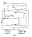
- Figure 1 is a block schematic diagram of one unit of the apparatus in use with multiple data processors; and
- Figure 2 is a connection diagram showing the interconnection of the two units of the apparatus to multiple data processors.
- Referring to Figure 1 the apparatus referred to hereinafter as an
interrupt logic unit 1 handles interrupt signals generated by telephone exchange apparatus for example (not shown) which signals are received by way of a number of inputs 20 to 2x. The interrupt signals are stored by theinterrupt logic unit 1 and forwarded to one ofN data processors 30 to 3N either immediately (immediate interrupt) or subsequently (non-immediate interrupt). - To this end each interrupt received as a signal on one of the inputs 20 to 2x is latched in an
interrupt store 2 and is passed to control logic 3 (which may be a microprocessor) by way of a data highway 4. Thecontrol logic 3 is arranged to be pre-programmed by the operating system of the multiple data processor arrangement (30 to 3N) with data defining which interrupts are enabled and which of the interrupts should give rise to an immediate interruption of the software running in one of the data processors. The aforementioned operating system also designates which of the N data processors will next handle interrupts. - Thus interrupts which are received by the
interrupt logic 1 unit are latched into theinterrupt store 2 and are compared by thecontrol logic 3 with the above criteria. An interrupt which is not enabled as aforesaid is handled by thecontrol logic 3 as a non-immediate interrupt. This facility permits unused ones of the inputs 20 to 2x to be left for future expansion, and unconnected, any such apparent interrupt signal being due possibly to "noise". - Some of the inputs 20 to 2x may also be programmed as not enabled when for example apparatus to which they are connected has been removed for servicing. However, if on comparison in the
control logic 3 the particular interrupt is determined as enabled a further comparison is carried out to determine if the input is an immediate interrupt. If the interrupt is non-immediate no further action is taken by thecontrol logic 3 for the time being. - If now a signal received on one of the inputs 20 to 2x is determined as being an immediate interrupt the
control logic 3 forwards an immediate interrupt signal to the previously designated one of thedata processors 30 to 3N on a respective one of theleads 60 to 6N. - On receipt of an interrupt signal the data processor selected (say) 30 stops running its present program and calls an interrupt handling program. The interrupt handling program initiates a read function which causes data to be transferred from the
interrupt store 2 to theread register 5 and latches the data in theread register 5 to prevent alteration of the data while the data processor is performing the read which causes the contents of the register to be transferred over the data bus 9 which is an input/output bus of the data processor system. On completion of the read function the data set in theinterrupt store 2 is cleared. - It is here noted that if the number of interrupt inputs 20 to 2x is greater than the number of highways in the data bus 9 a number of
read registers 5 may be provided and each may be addressed in turn by the interrupt handling program of thedata processor 30. - When the
register 5 is read the signals therefrom pass by way of theAND gates 80 to 8x which are held enabled by the signal on the lead 7 from thecontrol logic 3 and are fed back to theinterrupt store 2 as latch resetting signals. Thus only those interrupt signals which have been successfully transferred are cancelled in theinterrupt store 2, such signals arriving after latching of the readregister 5 being retained for comparison in the control logic. - Once the interrupts have been transferred from the
interrupt logic 1 the control logic disables theAND gates 80 to 8x and removes the latching signal from theread register 5. Further interrupt signals received at the inputs 20 to 2x are now similarly handled. - In normal operation, once one of the
data processors 30 to 3N has been interrupted, the multiple data processor operating system will access thecontrol logic 3 by way of the data bus 9 and change the data which designates the data processor to be interrupted. - As a further safeguard the
control logic 3 may be arranged to commence a timeout once it has applied an interrupt signal on one of theleads 60 to 6N. If theread register 5 has not been addressed before expiry of the timeout then thecontrol logic 3 is arranged to attempt to interrupt all of thedata processors 30 to 3N in turn until a response is received. It is here noted that the timeout may be pre-set in thecontrol logic 3 by the operating system by way of the data bus 9. It should also be noted that if the timeout above expires thecontrol logic 3 will generate interrupt data of its own into the interrupt store which the data processor successfully interrupted will read as part of its read function and which will cause an indication of the failure if required. - Turning now to Figure 2 for security purposes the
interrupt logic unit 1 of Figure 1 is duplicated, each of the logic units having the ability to interrupt any of thedata processors 30 to 3N by way of respective interrupt leads 60 to 6N. For the purposes of description the interrupt logic unit on the left of Figure 2 and its associated interrupts are designated as for Figure 1 whilst their equivalents on the right of Figure 2 are similarly designated with the addition of a prime ('). - Each of the
interrupt logic units 1 operates in an identical manner as far as determining the validity and status of an input signal received on one of the inputs 20 to 2x is concerned. In the case of Figure 2 however, one of the logic units, say, 1 is designated by the multiple data processor operating system as the "working" unit whilst the other logic unit 1' is designated as the "stand-by" unit. - The two
logic units 1 are interconnected with two respectiveadditional leads working logic unit 1 generates an interrupt on one of theleads 60 to 6N it will forward a signal on thelead 11 and when thelogic unit 1 detects that the read register (5 of Figure 1) has been read it forwards a signal on thelead 12. - On receipt of an immediate interrupt the standby interrupt logic unit 1' commences a timeout and monitors the
lead 11. This timeout may be preset by the operating system as previously described. Theinterrupt logic unit 1 having received the same immediate interrupt will proceed to pass a signal to one of theleads 60 to 6N and at the same time signals thelead 11. - The signal on the
lead 11 is detected by the interrupt logic unit 1' which then cancels the timeout. The interrupt logic unit 1' now starts a further timeout and monitors thelead 12. When theinterrupt logic unit 1 detects that the interrupted data processor say, 30 has read the interrupt data from theregister 5 it forwards a signal on thelead 12 which is detected by the interrupt logic unit 1' which then cancels the second timeout thus completing the monitoring sequence. - If either of the timeouts expires without receipt of the respective signals on the
leads interrupt logic unit 1. - It is here noted that if whilst a first immediate interrupt and accumulated non-immediate interrupts are being transferred, a second immediate interrupt is received, the interrupt
logic units 1, 1' will handle it on clearance of the read register. Thus if an immediate interrupt is received whilst the standby interrupt logic unit is monitoring thelead 12, the first monitoring timeout is also reset on detection of a signal on that lead. - The
control logic 3 of the interruptlogic units 1 are arranged to receive a periodic 'refresh' signal by way of the data bus 9. This periodic refresh signal which should be provided by the multiple data processor operating system is used to reset a timeout in thecontrol logic 3. If such a signal is not received prior to the expiry of the timeout the control logic generates an immediate interrupt. The interruptlogic unit 1 may also be arranged to cause a hardware alarm system (not shown) to operate. - The designation of the interrupt
logic units 1, 1' as "working" and "standby" respectively is periodically reversed by the multiple data processor operating system to ensure that each is fully functional should one be required to act as the sole interrupt logic unit if the other is temporarily unavailable.
Claims (8)
Applications Claiming Priority (2)
| Application Number | Priority Date | Filing Date | Title |
|---|---|---|---|
| GB8310003 | 1983-04-13 | ||
| GB838310003A GB8310003D0 (en) | 1983-04-13 | 1983-04-13 | Input signal handling apparatus |
Publications (2)
| Publication Number | Publication Date |
|---|---|
| EP0125797A1 EP0125797A1 (en) | 1984-11-21 |
| EP0125797B1 true EP0125797B1 (en) | 1987-10-14 |
Family
ID=10541038
Family Applications (1)
| Application Number | Title | Priority Date | Filing Date |
|---|---|---|---|
| EP84302530A Expired EP0125797B1 (en) | 1983-04-13 | 1984-04-13 | Interrupt signal handling apparatus |
Country Status (8)
| Country | Link |
|---|---|
| US (1) | US4638432A (en) |
| EP (1) | EP0125797B1 (en) |
| AU (1) | AU562586B2 (en) |
| CA (1) | CA1212478A (en) |
| DE (1) | DE3466813D1 (en) |
| GB (2) | GB8310003D0 (en) |
| NZ (1) | NZ207809A (en) |
| ZA (1) | ZA842713B (en) |
Families Citing this family (11)
| Publication number | Priority date | Publication date | Assignee | Title |
|---|---|---|---|---|
| CH670714A5 (en) * | 1986-10-22 | 1989-06-30 | Bbc Brown Boveri & Cie | |
| US4816990A (en) * | 1986-11-05 | 1989-03-28 | Stratus Computer, Inc. | Method and apparatus for fault-tolerant computer system having expandable processor section |
| US4959781A (en) * | 1988-05-16 | 1990-09-25 | Stardent Computer, Inc. | System for assigning interrupts to least busy processor that already loaded same class of interrupt routines |
| US5247685A (en) * | 1989-11-03 | 1993-09-21 | Compaq Computer Corp. | Interrupt handling in an asymmetric multiprocessor computer system |
| CA2026770A1 (en) * | 1989-11-03 | 1991-05-04 | John A. Landry | Multiprocessor interrupt control |
| US5291608A (en) * | 1990-02-13 | 1994-03-01 | International Business Machines Corporation | Display adapter event handler with rendering context manager |
| US5517624A (en) * | 1992-10-02 | 1996-05-14 | Compaq Computer Corporation | Multiplexed communication protocol between central and distributed peripherals in multiprocessor computer systems |
| US5435001A (en) * | 1993-07-06 | 1995-07-18 | Tandem Computers Incorporated | Method of state determination in lock-stepped processors |
| US6816934B2 (en) | 2000-12-22 | 2004-11-09 | Hewlett-Packard Development Company, L.P. | Computer system with registered peripheral component interconnect device for processing extended commands and attributes according to a registered peripheral component interconnect protocol |
| US6971043B2 (en) * | 2001-04-11 | 2005-11-29 | Stratus Technologies Bermuda Ltd | Apparatus and method for accessing a mass storage device in a fault-tolerant server |
| JP4182948B2 (en) * | 2004-12-21 | 2008-11-19 | 日本電気株式会社 | Fault tolerant computer system and interrupt control method therefor |
Family Cites Families (8)
| Publication number | Priority date | Publication date | Assignee | Title |
|---|---|---|---|---|
| US3716837A (en) * | 1971-04-22 | 1973-02-13 | Ibm | Interrupt handling |
| GB1425173A (en) * | 1972-05-03 | 1976-02-18 | Gen Electric Co Ltd | Data processing systems |
| US3908099A (en) * | 1974-09-27 | 1975-09-23 | Gte Automatic Electric Lab Inc | Fault detection system for a telephone exchange |
| US4270168A (en) * | 1978-08-31 | 1981-05-26 | United Technologies Corporation | Selective disablement in fail-operational, fail-safe multi-computer control system |
| JPS5537641A (en) * | 1978-09-08 | 1980-03-15 | Fujitsu Ltd | Synchronization system for doubled processor |
| US4268906A (en) * | 1978-12-22 | 1981-05-19 | International Business Machines Corporation | Data processor input/output controller |
| US4330826A (en) * | 1980-02-05 | 1982-05-18 | The Bendix Corporation | Synchronizer and synchronization system for a multiple computer system |
| US4371754A (en) * | 1980-11-19 | 1983-02-01 | Rockwell International Corporation | Automatic fault recovery system for a multiple processor telecommunications switching control |
-
1983
- 1983-04-13 GB GB838310003A patent/GB8310003D0/en active Pending
-
1984
- 1984-04-09 US US06/598,469 patent/US4638432A/en not_active Expired - Fee Related
- 1984-04-11 NZ NZ207809A patent/NZ207809A/en unknown
- 1984-04-12 AU AU26765/84A patent/AU562586B2/en not_active Ceased
- 1984-04-12 CA CA000451839A patent/CA1212478A/en not_active Expired
- 1984-04-12 ZA ZA842713A patent/ZA842713B/en unknown
- 1984-04-13 EP EP84302530A patent/EP0125797B1/en not_active Expired
- 1984-04-13 GB GB08409719A patent/GB2139786B/en not_active Expired
- 1984-04-13 DE DE8484302530T patent/DE3466813D1/en not_active Expired
Non-Patent Citations (1)
| Title |
|---|
| Automatic Control, December 1959, pages 46-52 * |
Also Published As
| Publication number | Publication date |
|---|---|
| ZA842713B (en) | 1984-12-24 |
| CA1212478A (en) | 1986-10-07 |
| DE3466813D1 (en) | 1987-11-19 |
| AU562586B2 (en) | 1987-06-11 |
| GB8310003D0 (en) | 1983-05-18 |
| US4638432A (en) | 1987-01-20 |
| GB8409719D0 (en) | 1984-05-23 |
| GB2139786B (en) | 1986-09-24 |
| NZ207809A (en) | 1988-02-29 |
| GB2139786A (en) | 1984-11-14 |
| AU2676584A (en) | 1984-10-18 |
| EP0125797A1 (en) | 1984-11-21 |
Similar Documents
| Publication | Publication Date | Title |
|---|---|---|
| EP0479230B1 (en) | Recovery method and apparatus for a pipelined processing unit of a multiprocessor system | |
| US4351023A (en) | Process control system with improved system security features | |
| EP0505706B1 (en) | Alternate processor continuation of the task of a failed processor | |
| KR920003497B1 (en) | Access loss processing system and its protection method | |
| US5948112A (en) | Method and apparatus for recovering from software faults | |
| EP0664511A2 (en) | Microprocessor fault log | |
| JPH0652506B2 (en) | Checkpoint retry mechanism | |
| JPH04338849A (en) | Excessive error correction method | |
| US4045661A (en) | Apparatus for detecting and processing errors | |
| JP3481737B2 (en) | Dump collection device and dump collection method | |
| JPH05225067A (en) | Important-memory-information protecting device | |
| US4638432A (en) | Apparatus for controlling the transfer of interrupt signals in data processors | |
| JP2956849B2 (en) | Data processing system | |
| EP0509479B1 (en) | Multiprocessor system | |
| CA1316608C (en) | Arrangement for error recovery in a self-guarding data processing system | |
| JP2937857B2 (en) | Lock flag release method and method for common storage | |
| JP2870202B2 (en) | Method and apparatus for mutual monitoring between processors | |
| JPH06214831A (en) | Abnormality detector for central processing unit | |
| KR19990057809A (en) | Error prevention system | |
| JP2776815B2 (en) | Failure recovery method for multiprocessor system | |
| JPS5827538B2 (en) | Mutual monitoring method | |
| JPH0695974A (en) | Memory protection method | |
| JP3110124B2 (en) | Failure detection method in multi-computer system | |
| JPH07117902B2 (en) | Rebooting device for information processing equipment | |
| JPH0713792A (en) | Error control system in hot standby system |
Legal Events
| Date | Code | Title | Description |
|---|---|---|---|
| PUAI | Public reference made under article 153(3) epc to a published international application that has entered the european phase |
Free format text: ORIGINAL CODE: 0009012 |
|
| AK | Designated contracting states |
Designated state(s): DE FR NL SE |
|
| 17P | Request for examination filed |
Effective date: 19841205 |
|
| GRAA | (expected) grant |
Free format text: ORIGINAL CODE: 0009210 |
|
| AK | Designated contracting states |
Kind code of ref document: B1 Designated state(s): DE FR NL SE |
|
| REF | Corresponds to: |
Ref document number: 3466813 Country of ref document: DE Date of ref document: 19871119 |
|
| ET | Fr: translation filed | ||
| PLBE | No opposition filed within time limit |
Free format text: ORIGINAL CODE: 0009261 |
|
| STAA | Information on the status of an ep patent application or granted ep patent |
Free format text: STATUS: NO OPPOSITION FILED WITHIN TIME LIMIT |
|
| 26N | No opposition filed | ||
| NLS | Nl: assignments of ep-patents |
Owner name: GEC PLESSEY TELECOMMUNICATIONS LIMITED TE COVENTRY |
|
| REG | Reference to a national code |
Ref country code: FR Ref legal event code: TP |
|
| NLS | Nl: assignments of ep-patents |
Owner name: GEC PLESSEY TELECOMMUNICATIONS LIMITED TE COVENTRY |
|
| NLT1 | Nl: modifications of names registered in virtue of documents presented to the patent office pursuant to art. 16 a, paragraph 1 |
Owner name: GPT INTERNATIONAL LIMITED TE COVENTRY, GROOT-BRITT |
|
| PGFP | Annual fee paid to national office [announced via postgrant information from national office to epo] |
Ref country code: FR Payment date: 19920408 Year of fee payment: 9 |
|
| PGFP | Annual fee paid to national office [announced via postgrant information from national office to epo] |
Ref country code: SE Payment date: 19920416 Year of fee payment: 9 |
|
| PGFP | Annual fee paid to national office [announced via postgrant information from national office to epo] |
Ref country code: NL Payment date: 19920430 Year of fee payment: 9 |
|
| PGFP | Annual fee paid to national office [announced via postgrant information from national office to epo] |
Ref country code: DE Payment date: 19920514 Year of fee payment: 9 |
|
| PG25 | Lapsed in a contracting state [announced via postgrant information from national office to epo] |
Ref country code: SE Effective date: 19930414 |
|
| PG25 | Lapsed in a contracting state [announced via postgrant information from national office to epo] |
Ref country code: NL Effective date: 19931101 |
|
| NLV4 | Nl: lapsed or anulled due to non-payment of the annual fee | ||
| PG25 | Lapsed in a contracting state [announced via postgrant information from national office to epo] |
Ref country code: FR Effective date: 19931229 |
|
| PG25 | Lapsed in a contracting state [announced via postgrant information from national office to epo] |
Ref country code: DE Effective date: 19940101 |
|
| REG | Reference to a national code |
Ref country code: FR Ref legal event code: ST |
|
| EUG | Se: european patent has lapsed |
Ref document number: 84302530.5 Effective date: 19931110 |