EP0125451A2 - Halbleiteranordnung in einem Mikrowellen-Hohlraumoszillator - Google Patents
Halbleiteranordnung in einem Mikrowellen-Hohlraumoszillator Download PDFInfo
- Publication number
- EP0125451A2 EP0125451A2 EP84103598A EP84103598A EP0125451A2 EP 0125451 A2 EP0125451 A2 EP 0125451A2 EP 84103598 A EP84103598 A EP 84103598A EP 84103598 A EP84103598 A EP 84103598A EP 0125451 A2 EP0125451 A2 EP 0125451A2
- Authority
- EP
- European Patent Office
- Prior art keywords
- carrier
- cavity
- oscillator
- substrate
- hole
- Prior art date
- Legal status (The legal status is an assumption and is not a legal conclusion. Google has not performed a legal analysis and makes no representation as to the accuracy of the status listed.)
- Granted
Links
Images

Classifications
-
- H—ELECTRICITY
- H03—ELECTRONIC CIRCUITRY
- H03B—GENERATION OF OSCILLATIONS, DIRECTLY OR BY FREQUENCY-CHANGING, BY CIRCUITS EMPLOYING ACTIVE ELEMENTS WHICH OPERATE IN A NON-SWITCHING MANNER; GENERATION OF NOISE BY SUCH CIRCUITS
- H03B5/00—Generation of oscillations using amplifier with regenerative feedback from output to input
- H03B5/18—Generation of oscillations using amplifier with regenerative feedback from output to input with frequency-determining element comprising distributed inductance and capacitance
- H03B5/1817—Generation of oscillations using amplifier with regenerative feedback from output to input with frequency-determining element comprising distributed inductance and capacitance the frequency-determining element being a cavity resonator
- H03B5/1823—Generation of oscillations using amplifier with regenerative feedback from output to input with frequency-determining element comprising distributed inductance and capacitance the frequency-determining element being a cavity resonator the active element in the amplifier being a semiconductor device
-
- H—ELECTRICITY
- H03—ELECTRONIC CIRCUITRY
- H03B—GENERATION OF OSCILLATIONS, DIRECTLY OR BY FREQUENCY-CHANGING, BY CIRCUITS EMPLOYING ACTIVE ELEMENTS WHICH OPERATE IN A NON-SWITCHING MANNER; GENERATION OF NOISE BY SUCH CIRCUITS
- H03B2201/00—Aspects of oscillators relating to varying the frequency of the oscillations
- H03B2201/01—Varying the frequency of the oscillations by manual means
- H03B2201/014—Varying the frequency of the oscillations by manual means the means being associated with an element comprising distributed inductances and capacitances
- H03B2201/015—Varying the frequency of the oscillations by manual means the means being associated with an element comprising distributed inductances and capacitances the element being a cavity
Definitions
- the invention relates to microwave cavity oscillators and in particular to mounting arrangements for mounting a semiconductor device, such as an excitation transistor, in a microwave cavity oscillator.
- Embodiments of the invention are especially applicable to transistor mounting arrangements for negative resistance microwave cavity oscillators.
- the transistor is coupled to a probe which extends into the cavity.
- the transistor is soldered directly to the wall of the cavity with one of its leads trimmed to serve as the probe. This has not been entirely satisfactory for various reasons. For example, it is difficult to optimise the transistor circuitry when the transistor is installed, and usually not practical to adjust the transistor circuitry before installation because of changes in circuit parameters due to slight inaccuracies in the lengths of connecting leads, which are determined only during final installation.
- a microwave cavity oscillator comprising:
- An advantage of such an arrangement is that the carrier and substrate can be assembled into a test chamber duplicating the characteristics of the microwave cavity and chamber and circuit adjustments, such as fine RF tuning and DC bias adjustments can be carried out.
- the sub-assembly can then be transferred to the housing and no further adjustments will usually be required. If they are, the sub-assembly can be removed while they are made, which greatly facilitates adjustments.
- the semiconductor device may be coupled to the cavity by a probe extending through the hole and a short distance into the cavity.
- the probe may be an extension of the substrate itself forming a flat capacitive coupling probe.
- the carrier may be an elongate member located at one end spigot-and-socket fashion in a socket or recess in the wall surrounding the hole. Its opposite end may then be supported at the opposite wall of the chamber.
- spring means is provided at said opposite end for urging the carrier into the socket or recess, to abut against the bottom thereof or for a surrounding shoulder to abut against the wall surrounding the recess. This assures accurate axial positioning of the carrier and hence of the substrate, semiconductor device and probe (where applicable).
- Support means for said opposite end of the carrier may comprise a screw-threaded bush engaged in a threaded hole in the said opposite wall of the chamber.
- the bush may be adapted at one end to supportingly engage the end of the carrier, conveniently in spigot-and-socket fashion, and adapted at the other end to engage a screwdriver, socket wrench or other such implement for screwing the bush into the hole.
- the carrier is of generally segmented cylindrical form and the substrate is a planar member mounted upon the chordal surface of the carrier.
- One cylindrical end portion of the carrier is then in the form of a ring.
- the semiconductor device is mounted on a part of the substrate in the ring and conveniently soldered to the interior of the ring, which extends over the device.
- the ring grounds the device and serves also as a heat sink.
- the ring also acts as a shield to reduce the susceptibility to stray couplings affecting the tuning when the sub-assembly is substituted.
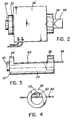
- the negative resistance cavity oscillator comprises an elongate block of aluminum 10 having a cavity 12 and a chamber 14 formed side-by-side within it and both opening onto the same one of the elongate surfaces of the block 10.
- a plate 16 also of aluminum, is affixed to that surface by any suitable means to seal the chamber 14 and the cavity 12.
- the cavity 12 and chamber 14 are of parallelepiped shape and separated by a dividing wall 18.
- a tuner 20 protrudes into the cavity from its sidewall opposed to the dividing wall 18.
- the tuner 20 does not comprise part of the present invention and so is not described in detail. It is the subject of copending patent application serial number( ).
- An output probe 19 extends through wall 18 and is coupled in chamber 14 to a drop-in isolator 21 in a recess in the bottom of chamber 14.
- a round hole 22 extends through the wall 18 at a position slightly more than half way from the base of the chamber 14.
- the surface of wall 18 in the chamber 14 has a circular recess 24, in the form of a counterbore, around the hole 22.
- a hole 26, coaxial with hole 22, extends through the end wall 28 of chamber 14, i.e. the wall opposite to dividing wall 18.
- the hole 26 is screwthreaded and an externally screwthreaded bush 30 is engaged in the hole 26.
- a carrier member 32 Suspended between the bush 30 and recess 24 is a carrier member 32.
- the carrier 32 has a segmented, specifically semi-cylindrical, portion 34 extending for most of its length and terminating in short, full-cylindrical end portions 36 and 38, respectively.
- the end surface of end portion 36 is formed with a spigot 40, dimensioned to fit snugly in the end of an axial hole 42 through the bush 30.
- a conical spring washer 44 is shown ( Figure 1) fitted over the spigot 40 to act between the annular end surfaces of the bush 30 and end portion 36, respectively.
- the opposite end portion 38 is a snug fit in the recess 24 in the dividing wall 18.
- the carrier 32 is made of gold-plated brass, or any other suitable material.
- the carrier member 32 carries a substrate 42 in the form of a plate of dielectric material copperplated both sides.
- the substrate 42 comprises a rectangular part 44 which rests upon the planar chordal surface of semi-cylindrical portion 34 of carrier 32, and overhangs its diameter.
- the substrate 42 is soldered to the carrier 32.
- a small rectangular extension 46 extends from the middle of that edge of the substrate portion 44 adjacent the carrier end portion 38. End portion 38 is hollowed so as to form a ring.
- the substrate extension 46 extends through the ring and its extremity projects a short distance beyond the end of the carrier 32 and into the cavity 12. This extremity portion is plated, preferably both sides to form a flat capacitive coupling probe 48.
- the substrate 42 carries a microwave semiconductor device in the form of transistor 50, in common collector package, which serves to excite the cavity 12 to oscillation.
- the substrate also carries associated circuit components such as RF tuning and DC bias circuitry (not shown).
- RF biasing chokes and decoupling capacitors are printed on the substrate.
- DC biasing and filtering components are mounted on the substrate after it has been soldered to the carrier 32.
- the transistor 50 is mounted on the part of the substrate 42 inside the ring 38.
- the transistor 50 has its base connected to the probe 48 and its emitter connected to the above-mentioned circuitry, which is carried by the main portion 44 of the substrate 42.
- the collector of the transistor is connected to ground simply by soldering the body of the transistor directly to the adjacent underside of the ring 38, as at 52.
- the carrier may readily be installed by locating the end portion 38 in the recess 24 and screwing the bush 30 into the chamber 14 to locate on the spigot 40.
- the outer end of the hole 42 is formed hexagonally to receive a suitable key to rotate the bush 30.
- the bush compresses the conical washer which urges the carrier 32 firmly and positively into the desired position.
- Accurate location of the carrier results from its end abutting firmly against the wall 18. This also provides corresponding accurate location of the transistor 50 and probe 48 relative to the cavity 12.
- An advantage of the described mounting arrangement is that it combines multiple functions, namely transistor mounting, heat sinking, RF coupling, RF tuning, DC biasing and filtering in a simple, compact, low-cost assembly. Moreover, tuning can readily be effected by filing the end of the probe or by adding solder to it.
- the specific embodiment is intended for use with bipolar transistors operating in the 4 and 6 GHz communication bands. It is envisaged, however, that the arrangement could be used with other semiconductor devices, for example field effect transistors or two terminal devices such as Gunn or Impatt diodes; and at other frequencies.
Landscapes
- Inductance-Capacitance Distribution Constants And Capacitance-Resistance Oscillators (AREA)
- Testing Of Individual Semiconductor Devices (AREA)
- Control Of Motors That Do Not Use Commutators (AREA)
Priority Applications (1)
| Application Number | Priority Date | Filing Date | Title |
|---|---|---|---|
| AT84103598T ATE38921T1 (de) | 1983-05-16 | 1984-03-31 | Halbleiteranordnung in einem mikrowellenhohlraumoszillator. |
Applications Claiming Priority (2)
| Application Number | Priority Date | Filing Date | Title |
|---|---|---|---|
| CA000428269A CA1189581A (en) | 1983-05-16 | 1983-05-16 | Mounting a semiconductor device in a microwave cavity oscillator |
| CA428269 | 1983-05-16 |
Publications (3)
| Publication Number | Publication Date |
|---|---|
| EP0125451A2 true EP0125451A2 (de) | 1984-11-21 |
| EP0125451A3 EP0125451A3 (en) | 1985-11-27 |
| EP0125451B1 EP0125451B1 (de) | 1988-11-23 |
Family
ID=4125256
Family Applications (1)
| Application Number | Title | Priority Date | Filing Date |
|---|---|---|---|
| EP84103598A Expired EP0125451B1 (de) | 1983-05-16 | 1984-03-31 | Halbleiteranordnung in einem Mikrowellen-Hohlraumoszillator |
Country Status (6)
| Country | Link |
|---|---|
| US (1) | US4556852A (de) |
| EP (1) | EP0125451B1 (de) |
| JP (1) | JPS59221010A (de) |
| AT (1) | ATE38921T1 (de) |
| CA (1) | CA1189581A (de) |
| DE (1) | DE3475367D1 (de) |
Families Citing this family (1)
| Publication number | Priority date | Publication date | Assignee | Title |
|---|---|---|---|---|
| RU2217860C2 (ru) * | 2001-11-12 | 2003-11-27 | Институт лазерной физики СО РАН | Генератор электромагнитных колебаний |
Family Cites Families (4)
| Publication number | Priority date | Publication date | Assignee | Title |
|---|---|---|---|---|
| SE383595B (sv) * | 1974-09-09 | 1976-03-15 | Incentive Ab | Mikrovagsoscillator |
| JPS5927122B2 (ja) * | 1978-11-22 | 1984-07-03 | 三菱電機株式会社 | マイクロ波集積回路装置 |
| DE2851870A1 (de) * | 1978-11-30 | 1980-06-04 | Siemens Ag | Mikrowellen-netzwerk mit einer temperaturkompensation |
| DD148421A1 (de) * | 1979-12-27 | 1981-05-20 | Westphal Klaus Dieter | Schaltungsanordnung fuer mikrowellenoszillatoren |
-
1983
- 1983-05-16 CA CA000428269A patent/CA1189581A/en not_active Expired
- 1983-09-19 US US06/533,356 patent/US4556852A/en not_active Expired - Lifetime
-
1984
- 1984-03-31 AT AT84103598T patent/ATE38921T1/de not_active IP Right Cessation
- 1984-03-31 EP EP84103598A patent/EP0125451B1/de not_active Expired
- 1984-03-31 DE DE8484103598T patent/DE3475367D1/de not_active Expired
- 1984-05-16 JP JP59096745A patent/JPS59221010A/ja active Granted
Also Published As
| Publication number | Publication date |
|---|---|
| JPS59221010A (ja) | 1984-12-12 |
| JPH0464202B2 (de) | 1992-10-14 |
| CA1189581A (en) | 1985-06-25 |
| US4556852A (en) | 1985-12-03 |
| DE3475367D1 (en) | 1988-12-29 |
| EP0125451B1 (de) | 1988-11-23 |
| EP0125451A3 (en) | 1985-11-27 |
| ATE38921T1 (de) | 1988-12-15 |
Similar Documents
| Publication | Publication Date | Title |
|---|---|---|
| US4628283A (en) | Hermetically sealed oscillator with dielectric resonator tuned through dielectric window by adjusting screw | |
| US5309163A (en) | Active patch antenna transmitter | |
| EP0399770A1 (de) | Vorrichtung mit dielektrischem Resonator | |
| EP0394375B1 (de) | Packungseinrichtung für diodenanordnung | |
| US4477788A (en) | Dielectric resonator tuner and mechanical mounting system | |
| US4556852A (en) | Mounting a semiconductor device in a microwave cavity oscillator | |
| US4097821A (en) | Coaxial line IMPATT diode oscillator | |
| CA1115361A (en) | Microwave oscillator for microwave integrated circuit applications | |
| US4172240A (en) | Cylindrical cavity power combiner for a plurality of coaxial oscillators | |
| US3996529A (en) | Varactor tuning apparatus for a strip transmission line device | |
| US4097823A (en) | Transmitter wherein outputs of a plurality of pulse modulated diode oscillators are combined | |
| CA1210461A (en) | Microwave oscillator | |
| US3801882A (en) | Thermo-electric mounting method for rf silicon power transistors | |
| US4228539A (en) | High frequency transmitter | |
| US4862111A (en) | Microwave oscillator having a dielectric resonator, in particular for the 22 GHz range | |
| US4990865A (en) | Transistor microwave oscillator having adjustable zone of potential instability | |
| US3681718A (en) | Millimeter wave translating device with changeable insert element | |
| US3775701A (en) | Semiconductor diode mounting and resonator structure for operation in the ehf microwave range | |
| US4912402A (en) | Fixture for measuring the static characteristics of microwave three-terminal active components | |
| US3792374A (en) | Wideband mechanically and electronically tuned negative resistance oscillator | |
| US4588967A (en) | Integrated varactor tuned coaxial gun oscillator for 60 GHz operation | |
| EP0125449A2 (de) | Mirkowelleneinrichtung mit Blendenkupplung | |
| GB1427240A (en) | Microwace oscillator | |
| JP2581884Y2 (ja) | パッケージ | |
| US6879219B2 (en) | High frequency oscillator with vertical resonator |
Legal Events
| Date | Code | Title | Description |
|---|---|---|---|
| PUAI | Public reference made under article 153(3) epc to a published international application that has entered the european phase |
Free format text: ORIGINAL CODE: 0009012 |
|
| AK | Designated contracting states |
Designated state(s): AT DE FR GB NL SE |
|
| PUAL | Search report despatched |
Free format text: ORIGINAL CODE: 0009013 |
|
| AK | Designated contracting states |
Designated state(s): AT DE FR GB NL SE |
|
| 17P | Request for examination filed |
Effective date: 19860117 |
|
| 17Q | First examination report despatched |
Effective date: 19870511 |
|
| GRAA | (expected) grant |
Free format text: ORIGINAL CODE: 0009210 |
|
| AK | Designated contracting states |
Kind code of ref document: B1 Designated state(s): AT DE FR GB NL SE |
|
| REF | Corresponds to: |
Ref document number: 38921 Country of ref document: AT Date of ref document: 19881215 Kind code of ref document: T |
|
| REF | Corresponds to: |
Ref document number: 3475367 Country of ref document: DE Date of ref document: 19881229 |
|
| ET | Fr: translation filed | ||
| PLBE | No opposition filed within time limit |
Free format text: ORIGINAL CODE: 0009261 |
|
| STAA | Information on the status of an ep patent application or granted ep patent |
Free format text: STATUS: NO OPPOSITION FILED WITHIN TIME LIMIT |
|
| 26N | No opposition filed | ||
| PGFP | Annual fee paid to national office [announced via postgrant information from national office to epo] |
Ref country code: AT Payment date: 19920311 Year of fee payment: 9 |
|
| PGFP | Annual fee paid to national office [announced via postgrant information from national office to epo] |
Ref country code: SE Payment date: 19920319 Year of fee payment: 9 |
|
| PGFP | Annual fee paid to national office [announced via postgrant information from national office to epo] |
Ref country code: NL Payment date: 19920331 Year of fee payment: 9 |
|
| PG25 | Lapsed in a contracting state [announced via postgrant information from national office to epo] |
Ref country code: AT Effective date: 19930331 |
|
| PG25 | Lapsed in a contracting state [announced via postgrant information from national office to epo] |
Ref country code: SE Effective date: 19930401 |
|
| PG25 | Lapsed in a contracting state [announced via postgrant information from national office to epo] |
Ref country code: NL Effective date: 19931001 |
|
| NLV4 | Nl: lapsed or anulled due to non-payment of the annual fee | ||
| EUG | Se: european patent has lapsed |
Ref document number: 84103598.3 Effective date: 19931110 |
|
| PGFP | Annual fee paid to national office [announced via postgrant information from national office to epo] |
Ref country code: FR Payment date: 19980310 Year of fee payment: 15 |
|
| PGFP | Annual fee paid to national office [announced via postgrant information from national office to epo] |
Ref country code: GB Payment date: 19980323 Year of fee payment: 15 |
|
| PGFP | Annual fee paid to national office [announced via postgrant information from national office to epo] |
Ref country code: DE Payment date: 19980403 Year of fee payment: 15 |
|
| PG25 | Lapsed in a contracting state [announced via postgrant information from national office to epo] |
Ref country code: GB Free format text: LAPSE BECAUSE OF NON-PAYMENT OF DUE FEES Effective date: 19990331 |
|
| GBPC | Gb: european patent ceased through non-payment of renewal fee |
Effective date: 19990331 |
|
| PG25 | Lapsed in a contracting state [announced via postgrant information from national office to epo] |
Ref country code: FR Free format text: LAPSE BECAUSE OF NON-PAYMENT OF DUE FEES Effective date: 19991130 |
|
| REG | Reference to a national code |
Ref country code: FR Ref legal event code: ST |
|
| PG25 | Lapsed in a contracting state [announced via postgrant information from national office to epo] |
Ref country code: DE Free format text: LAPSE BECAUSE OF NON-PAYMENT OF DUE FEES Effective date: 20000101 |