EP0125317B1 - Method of controlling changeover of plurality of motors - Google Patents
Method of controlling changeover of plurality of motors Download PDFInfo
- Publication number
- EP0125317B1 EP0125317B1 EP83903572A EP83903572A EP0125317B1 EP 0125317 B1 EP0125317 B1 EP 0125317B1 EP 83903572 A EP83903572 A EP 83903572A EP 83903572 A EP83903572 A EP 83903572A EP 0125317 B1 EP0125317 B1 EP 0125317B1
- Authority
- EP
- European Patent Office
- Prior art keywords
- motors
- motor
- circuit
- servo control
- velocity error
- Prior art date
- Legal status (The legal status is an assumption and is not a legal conclusion. Google has not performed a legal analysis and makes no representation as to the accuracy of the status listed.)
- Expired - Lifetime
Links
Images


Classifications
-
- G—PHYSICS
- G05—CONTROLLING; REGULATING
- G05B—CONTROL OR REGULATING SYSTEMS IN GENERAL; FUNCTIONAL ELEMENTS OF SUCH SYSTEMS; MONITORING OR TESTING ARRANGEMENTS FOR SUCH SYSTEMS OR ELEMENTS
- G05B19/00—Program-control systems
- G05B19/02—Program-control systems electric
- G05B19/18—Numerical control [NC], i.e. automatically operating machines, in particular machine tools, e.g. in a manufacturing environment, so as to execute positioning, movement or co-ordinated operations by means of program data in numerical form
- G05B19/414—Structure of the control system, e.g. common controller or multiprocessor systems, interface to servo, programmable interface controller
- G05B19/4144—Structure of the control system, e.g. common controller or multiprocessor systems, interface to servo, programmable interface controller characterised by using multiplexing for control system
Definitions
- This invention relates to an electrical motor drive arrangement operable to drive a motor selected from a plurality of electrical motors having different maximum output powers, and further operable to switch the drive from one motor to another (see for example JP-U-54114008).
- a turning machining motor is driven when turning machining is performed, thereby to rotate a workpiece at a commanded rotational velocity to carry out the turning operation.
- a spindle is positioned at a predetermined point, upon which a motor for a rotary tool is driven to rotate the tool, thereby drilling a hole into the stationary workpiece.
- US ⁇ A ⁇ 4 240 016 discloses an industrial robot having a plurality of electrical drive motors for different axes of the robot. A single velocity unit is switched to a selected one of the motors in accordance with an axis selecting instruction read out from a memory. Here, however, the motors do not have different maximum output powers.
- an electrical motor drive arrangement operable to drive a motor selected from a plurality of electrical motors having different maximum output powers, and further operable to switch the drive from one motor to another, characterised in that the electrical motor drive arrangement comprises a single servo control circuit for driving successive ones of the motors, a power line switching circuit for switching the servo control circuit from one motor to the next, a signal line switching circuit for switching a velocity feedback input of the servo control circuit to the motor which is being driven, and a plurality of velocity error-amplitude command tables having characteristics corresponding to respective ones of the motors, the arrangement being operable to select from these tables the conversion table corresponding to the motor selected for operation, and to apply to the servo control circuit an amplitude command, retrieved from the selected table, corresponding to the velocity error (difference between actual and commanded velocities) detected forthe selected motor.
- a preferred embodiment of the present invention provides a plural motor changeover control system which makes it possible to commonly apply a control unit with ease, and which is simple in construction and low in cost.
- a preferred embodiment of the present invention provides a plural motor changeover control system which has a signal line switching circuit of a simple arrangement, and which is improved to dispense with the need for a driving power supply and a great amount of space.
- the signal line switching circuit may be constituted by an analog switch.
- a servo control circuit is commonly applied to enable changeover control of a plurality of motors having different outputs.
- a servo control circuit is commonly applied to enable changeover control of a plurality of motors having different outputs.
- commensurate amplitude, phase and slip commands may be applied.
- a resulting advantage is that an output torque characteristic can be satisfied by a small current corresponding to a velocity error.
- control is possible in accordance with optimum motor characteristics, such as generation and diminution of motor heat.
- the signal line switching circuit for applying the motor feedback signals to the servo control circuit may be constituted by an analog switch, an advantage gained is that a power supply for driving the switch need not be separately provided. Also, with semiconductor construction, little installation space is required and wiring is facilitated. Another practical advantage is that the power supply of the servo control circuit can be utilized.
- Fig.1 1 is a block diagram of an embodiment of the present invention
- Fig. 2 is a block diagram illustrating a principal portion of the arrangement of Fig. 1
- Fig. 3 is a view for describing the operation of the arrangement of Fig. 2
- Fig. 4 is a conversion table characteristic used in an embodiment of the present invention
- Fig. 5 is a view for describing a switching circuit arrangement of an embodiment of the present invention
- Fig. 6 is a view showing the details of a principal portion of the arrangement illustrated in Fig. 5.
- Fig. 1 is an overall block diagram of a control circuit embodying the present invention.
- numerals 1a, 1b denote three-phase induction motors.
- the induction motor 1a a rotates the spindle of a machine tool
- the induction motor 1b rotates a tool.
- Numerals 2a, 2b denote pulse generators for producing velocity pulses TSA in dependence upon rotation of the AC motors 1 a and 1 respectively.
- Numeral 3 designates an arithmetic circuit constituting part of a control section for the induction motors 1a, 1b.
- the arithmetic circuit 3 senses the actual velocity RV of the induction motors 1a, 1b on the basis of the velocity pulses TSA from the pulse generators 2a, 2b, and produces an amplitude command Id as well as U- and V-phase phase commands Ud, Vd in dependence upon the difference between the actual velocity and a commanded velocity CV.
- the arithmetic circuit 3 is composed of a processor 30 for performing processing, a program memory 31 storing a control program, a data memory 32 for storing various data, input/output ports 33, 34, a counter 35, and an address/data bus 36 interconnecting these components.
- the processor 30 retrieves a velocity error-amplitude command (ER-Id) conversion table, a velocity error-phase (ER- ⁇ ) conversion table, and a velocity error-slip frequency (ER-Ws) conversion table, these tables being provided in the data memory 32, and obtains a corresponding amplitude command Id, a corresponding phase ⁇ , and a corresponding slip frequency Ws.
- the processor 30 delivers the amplitude command Id to the input/output port 33 through the bus 36.
- the processor 30 retrieves an actual velocity-angular frequency (RV-Wo) conversion table from within the data memory 32, reads out a corresponding angular frequency Wo, calculates the U-phase phase command and the V-phase phase command reads out the U- and V-phase phase commands Ud, Vd, and delivers these commands to the input/output port 34 through the bus 36.
- RV-Wo velocity-angular frequency
- Numeral 4a denotes a digital/analog conversion circuit (DA circuit) for converting the digital amplitude command Id into an analog amplitude command Is.
- Numerals 4b, 4c denote multiplying-type digital/analog conversion circuits for converting the respective U- and V-phase current commands Ud, Vd into analog quantities and for multiplying these analog quantities by the analog amplitude command Is to produce analog U- and V-phase current commands lu, lv, respectively.
- Numeral 5 designates a W-phase current forming circuit for forming a W-phase current command Iw from the analog U- and V-phase current commands lu, lv.
- Numeral 6 represents an operational amplifier for obtaining the difference between actual phase currents and the commanded currents lu, Iv, Iw in the respective phases.
- the operational amplifier 6 is composed of an operational amplifier for calculating the difference between the commanded currents lu, lv, Iw in the respective phases, and the actual phase currents lau, lav, law, respectively, and an arithmetic circuit for producing a W-phase phase current law by adding lav and lau, which are sensed by current transformers 9a, 9b.
- Numeral 7 denotes a pulse-width modulating circuit
- numeral 8 an inverter controlled by an output signal from the pulse-width modulating circuit 7 for providing a DC voltage derived from an externally provided three-phase AC power supply and a rectifying circuit (a group of diodes and a capacitor) for rectifying the three-phase alternating current into a direct current.
- the pulse-width modulating circuit 7 includes a sawtooth waveform generating circuit STSG, comparators COMu, COMv, COMw, NOT gates NOT, through NOT 3 , drivers DV, through DV 6 .
- the inverter 8 includes six power transistors a1 through Q6 and six diodes D1 through D6.
- the comparators COMu, COMv, COMw of the pulse-width modulating circuit 7 compare a sawtooth signal STS with the amplitudes of the three-phase AC signals iu, iv, iw, respectively, and produce a "0" output when the magnitude of STS is exceeded by iu, iv or iw.
- the comparator COMu produces the current command i u c shown in Fig. 3. More specifically, pulse-width modulated three-phase current commands iuc, ivc, iwc dependent upon the amplitudes of iu, iv, iw are produced.
- Numeral 10 denotes a power line switching circuit for connecting the inverter 8 to the induction motor 1a by connecting contacts to the a side, and for connecting the inverter 8 to the induction motor 1 b by connecting the contacts to the b side.
- Numeral 11 designates a signal line switching circuit which, depending upon how switching is performed, connects either the pulse generator 2a or 2b to the counter 35 to apply the velocity pulses TSA, which are velocity feedback pulses, to the counter 35.
- the processor 30 of the arithmetic unit 3 reads the value in the counter 35, which counts the velocity pulses TSA, through the bus 36 to sense the actual velocity RV of the induction motor 1. Next, based on the error ER between the commanded velocity CV and the sensed actual velocity RV, the processor 30 retrieves the ER-Is, ER- ⁇ , and ER-Ws conversion tables from the data memory 32 obtains the amplitude command ld, the phase ⁇ and the slip frequency Ws, retrieves the RV-Wo conversion table from within the data memory 32, obtains the corresponding angular frequency Wo, calculates the U- and V-phase phase commands Ud, Vd and, via the bus 36, applies the amplitude command Id to the input/ output port circuit 33 and the U- and V-phase phase commands Ud, Vd to the input/output port circuit 34.
- the amplitude command Id from the input/output port 33 is converted into an analog amplitude command Is by the digital/analog conversion circuit 4a, which command is then applied to the multiplying-type digital/analog conversion circuits 4b, 4c.
- the U- and V-phase phase commands Ud, Vd are converted into analog quantities by the respective multiplying-type digital/analog conversion circuits 4b, 4c, which quantities are multiplied by the analog amplitude command Is to be converted into analog U- and V-phase current commands lu, lv.
- the U- and V-phase current commands lu, lv are applied to the W-phase current forming circuit 5, which produces the W-phase current lw.
- the W-phase current Iw is applied to the operational amplifier 6 together with the U- and V-phase current commands lu, Iv, respectively.
- the operational amplifier 6 receives the actual phase currents lau, lav from the converters 9a, 9b and forms the W-phase phase current law.
- the operational amplifier 6 also produces three-phase AC signals iu, iv, iw, which are the differences between the three-phase current commands lu, lv, lw and respective ones of the actual phase currents lau, lav, law.
- the three-phase AC signals iu, iv, iw indicative of these differences are applied to the respective comparators COMu, COMv, COMw of the pulse-width modulating circuit 7.
- the comparators COMu, COMv, COMw compare the amplitudes of the three-phase AC signals iu, iv, iw with the amplitude of the sawtooth signal STS, and deliver as outputs three-phase current commands iuc, ivc, iwc produced by way of pulse width modulation.
- the outputs from the comparators are supplied to the NOT gates NOT, through NOT 3 and to the drivers DV, through DV 6 , which generate the inverter drive signals SQ1 through SQ6.
- the inverter drive signals SQ1 through SQ6 are applied to the bases of the power transistors Q1 through Q6, respectively, in the inverter 8 to control the on/off action of the power transistors Q1 through Q6 for supplying three-phase current to the induction motor 1 a.
- the induction motor 1 a will thenceforth be controlled in a similar mode until the motor eventually rotates at the commanded velocity.
- the induction motor 1b is driven by a similar operation when the contacts of the power line switching circuit 10 are connected to the b side and the pulse generator 2b is connected to the counter 35 by the signal line switching circuit 11.
- the data memory 32 is provided with a conversion table 32a for the conversion from velocity error to amplitude, phase and slip for the induction motor 1a, and with a conversion table 32b for the conversion from velocity error to amplitude, phase and slip for the induction motor 1b.
- Either the conversion table 32a or 32b is selected in a shift-like manner in synchronism with the switching performed by the switching circuits 10, 11.
- This function is provided because the maximum outputs of the induction motors 1a, 1b differ from each other, and is for the purpose of delivering an amplitude command that corresponds to the maximum output. Specifically, if we assume that a current of 41 (A) prevails at the maximum velocity error of the induction motor 1 a and that a current of I (A) prevails at the maximum velocity error of the induction motor 1b, then the amplitude command Id in both cases will be E volts when the respective associated conversion table is used for each of the induction motors 1a, 1b. This amplitude command Id is applied as a voltage value.
- a maximum amplitude command E will correspond to a current of 41 (A) for the induction motor 1a, and to a current of I (A) for the induction motor 1 b.
- the feedback voltages, namely the actual phase current values, from the current sensors 9a, 9b will be 41R and IR, respectively, where R is the value of each current sensing resistor.
- a velocity error-amplitude command conversion table 32a having a characteristic of the kind indicated by A in Fig. 4 is provided for the induction motor 1a
- a velocity error-amplitude command conversion table 32b having a characteristic of the kind indicated by B in Fig. 4 is provided for the induction motor 1b.
- velocity error-phase and velocity error-slip frequency conversion tables corresponding to the characteristics of the induction motors 1a, 1 b are provided for each of these motors.
- the amplitude command voltage of, e.g., the induction motor 1a a when the maximum velocity error prevails will be E and that of the induction motor 1 b will be E/4, so that these will correspond to the aforementioned currents of 41, I, respectively.
- the feedback voltages from the current sensors will be 41R, IR, the ratio whereof will be the same as that of the abovementioned amplitude command voltages.
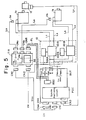
- Fig. 5 is a block diagram showing the details of a plural motor switching circuit arrangement according to the present invention.
- Fig. 6 is a view showing the details of a principal portion of the arrangement illustrated in Fig. 5.
- SUT represents a servo control circuit consisting of a printed circuit board on which there are mounted the components of the arithmetic circuit 3 of Fig. 1 with the exception of the data memory 32, the DA converters 4a through 4c, the W-phase current forming circuit 5, the operational amplifier 6, the pulse-width modulating circuit 7 and the inverter circuit 8.
- the servo control circuit SUT has a connector CN4 for receiving velocity commands and switching commands, etc., from a spindle control section of an external NC unit, and for the exchange of other data and commands, a connector CN1 for receiving a velocity command signal from a switching circuit described below, a connector CN3 for receiving a fixed velocity pulse from a position coder 12 via a line L7, output terminals U, V, W, G for U, V, W and G (ground) phases, which are the outputs of the inverter 8, and fan motor output terminals FMA, FMB.
- POC denotes a circuit for stopping a spindle at a predetermined position.
- the circuit POC receives the fixed velocity pulse applied through the connector CN3 and controls the stopping of the induction motor l a.
- the circuit is not illustrated in Fig. 1.
- Numeral 10 denotes the power line switching circuit of Fig. 1.
- the circuit has relays 100A, 100B, as well as electromagnetic contacts 101A, 101B, which correspond to the induction motors 1a, 1b.
- the circuit 10 connects or disconnects the output terminals U, V, W, G of the servo control circuit SUT and lines L1, L3, and connects or disconnects the fan motor output terminals FMA, FMB and lines L2, L4.
- Numeral 11A designates a cross board equipped with the signal line switching circuit 11 and the data memory 32 of the arithmetic circuit 32 shown in Fig. 1.
- the cross board 11A has a pair of analog switch groups 11a, 11 b, and the data memory 32 storing the abovementioned conversion tables.
- a switching control circuit 11c turns on either of the analog switch groups 11 a, 11b so that velocity pulses from pulse generator 2a or 2b are transmitted to the connector CN1 through connector CNa or CNb.
- the analog switch groups 11a, 11b each have analog switches AS (e.g., FETs) the number whereof corresponds to the number of lines (four in the illustration). These analog switches are operated by the power supply voltage provided by the servo control circuit SUT via a flat cable FL and a connector CNR.
- the data memory 32 which stores the conversion table 32a for the induction motor 1a and the conversion table 32b for the induction motor 1b, is connected via the connector CNR, flat cable F1 and a connector RSO to the bus 36 of the arithmetic circuit 3 mounted on the servo control circuit SUT.
- a switching signal SW for selecting the induction motor 1 a is provided by the NC unit, the signal is applied to the switching control circuit 11c (Fig. 6) through the connector CN2 to turn on each of the analog switches AS in the analog switch group 11a.
- relay 100A of the power line switching circuit 10 is actuated to turn on the electromagnetic contact 101A to connect the output terminals U, V, W, G of the servo control circuit SUT with the line L1, and to connect the output terminals FMA, FMB with the line L2.
- the switching signal SW enters the servo control circuit SUT through the connector CN2 and flat cable FL, so that the arithmetic circuit 30 selects the conversion table 32a of data memory 32 through the flat cable FL.
- the servo control circuit SUT based on the velocity command CV received through the connector CN4, and in accordance with the velocity pulses from the pulse generator 2a, retrieves the conversion table 32a of the data memory 32 through the flat cable FL, generates the drive currents in each phase at the output terminals U, V, W and G, and applies these to the induction motor 1a a through the line L1 to control the induction motor 1a in the manner described in connection with Fig. 1. Furthermore, the servo control circuit SUT delivers fan motor drive signal via line L2 to drive the fan motor of the induction motor 1a. When a switching signal SW for selecting the induction motor 1 b is applied, on the other hand, the foregoing operation is reversed.
- each of the analog switches AS in the analog switch group 11b is turned on.
- relay 100B of the power line switching circuit 10 is actuated to turn on the electromagnetic contact 101B to connect the output terminals U, V, W, G of the servo control circuit SUT with the line L3, and to connect the output terminals FMA, FMB with the line L4.
- the arithmetic circuit 30 selects the conversion table 32b of data memory 32 through the flat cable FL. Accordingly, the servo control circuit SUT, based on the velocity command CV received through the connector CN4, and in accordance with the velocity pulses from the pulse generator 2b, .
- the fan motor of the induction motor 1b is driven by a fan motor drive signal provided by the output terminals FMA, FMB of the servo control circuit SUT via the electromagnetic contact 101B and line L4. Since the cross panel 11A is thus constructed of analog switches, a power supply or the like for driving relays is unnecessary.
- the power line switching circuit 10 handles large currents and high-power drive signals and is constructed of relay circuitry since analog switches cannot be used owing to their low breakdown voltage.
- one and the same data memory 32 stores the conversion tables 32a, 32b having the motor characteristics for two induction motors.
- the two conversion tables can each be stored in a separate memory.
- the conversion tables are switched between by the processor 30 delivering a switching signal to the switching circuit 10 in accordance with a program.
- the switching operation can be performed in response to an externally applied switching signal.
- this can be accomplished by a switching operation performed after the power supply has been turned off once, or by a clearing operation performed by the processor 30.
- the present invention is well-suited for application to a numerically controlled machine tool equipped with a plurality of induction motors the outputs whereof differ.
- the invention is not limited to such application but can also be utilized in other equipment that include a servo mechanism, such as in robot mechanisms.
Landscapes
- Engineering & Computer Science (AREA)
- Human Computer Interaction (AREA)
- Manufacturing & Machinery (AREA)
- Physics & Mathematics (AREA)
- General Physics & Mathematics (AREA)
- Automation & Control Theory (AREA)
- Control Of Multiple Motors (AREA)
Abstract
Description
- This invention relates to an electrical motor drive arrangement operable to drive a motor selected from a plurality of electrical motors having different maximum output powers, and further operable to switch the drive from one motor to another (see for example JP-U-54114008).
- In a machine tool or the like equipped with a plurality of motors having different maximum output powers, the motors are driven alternately. Byway of example, in a turning center orthe like, a turning machining motor is driven when turning machining is performed, thereby to rotate a workpiece at a commanded rotational velocity to carry out the turning operation. When a screw hole, hole or keyway is to be formed after the turning operation, a spindle is positioned at a predetermined point, upon which a motor for a rotary tool is driven to rotate the tool, thereby drilling a hole into the stationary workpiece. Since the motor for the turning operation and the motor for the rotary tool are so arranged that while one is being driven the other is not, it has been contemplated to control the motors by a single servo control apparatus. If it were possible to apply such a servo control apparatus commonly for the two motors, the results would be very beneficial as it would make it possible to greatly simplify the arrangement and reduce the cost of the equipment. If the maximum outputs of the turning motor and rotary tool motor were identical, common application of the servo control apparatus would be very simple to achieve. In general, however, the maximum outputs of these motors differ by a wide margin, so that common application is difficult. Even if a servo control apparatus were to be applied to both motors, neither a significant simplification nor a significant reduction in cost would be achieved.
- Moreover, in order to achieve such common application, it would be necessary to provide a switching circuit for the signal lines that transmit feedback signals from the motors, in addition to a switching circuit for the power lines that transmit the motor drive signals. These switching circuits use separately installed switching units that rely upon relay circuits. When relays are used, however, it is necessary to provide a power supply for driving the relays. This requires a great amount of space and complicated wiring.
- US―A―4 240 016 discloses an industrial robot having a plurality of electrical drive motors for different axes of the robot. A single velocity unit is switched to a selected one of the motors in accordance with an axis selecting instruction read out from a memory. Here, however, the motors do not have different maximum output powers.
- According to the present invention there is provided an electrical motor drive arrangement operable to drive a motor selected from a plurality of electrical motors having different maximum output powers, and further operable to switch the drive from one motor to another, characterised in that the electrical motor drive arrangement comprises a single servo control circuit for driving successive ones of the motors, a power line switching circuit for switching the servo control circuit from one motor to the next, a signal line switching circuit for switching a velocity feedback input of the servo control circuit to the motor which is being driven, and a plurality of velocity error-amplitude command tables having characteristics corresponding to respective ones of the motors, the arrangement being operable to select from these tables the conversion table corresponding to the motor selected for operation, and to apply to the servo control circuit an amplitude command, retrieved from the selected table, corresponding to the velocity error (difference between actual and commanded velocities) detected forthe selected motor.
- A preferred embodiment of the present invention provides a plural motor changeover control system which makes it possible to commonly apply a control unit with ease, and which is simple in construction and low in cost.
- A preferred embodiment of the present invention provides a plural motor changeover control system which has a signal line switching circuit of a simple arrangement, and which is improved to dispense with the need for a driving power supply and a great amount of space.
- The signal line switching circuit may be constituted by an analog switch.
- According to the present invention, and % advantage is provided wherein a servo control circuit is commonly applied to enable changeover control of a plurality of motors having different outputs. In addition, to cope with motors for producing small outputs, commensurate amplitude, phase and slip commands may be applied. Accordingly, a resulting advantage is that an output torque characteristic can be satisfied by a small current corresponding to a velocity error. Further, control is possible in accordance with optimum motor characteristics, such as generation and diminution of motor heat. In addition, since the signal line switching circuit for applying the motor feedback signals to the servo control circuit may be constituted by an analog switch, an advantage gained is that a power supply for driving the switch need not be separately provided. Also, with semiconductor construction, little installation space is required and wiring is facilitated. Another practical advantage is that the power supply of the servo control circuit can be utilized.
- Fig.1 1 is a block diagram of an embodiment of the present invention, Fig. 2 is a block diagram illustrating a principal portion of the arrangement of Fig. 1, Fig. 3 is a view for describing the operation of the arrangement of Fig. 2, Fig. 4 is a conversion table characteristic used in an embodiment of the present invention, Fig. 5 is a view for describing a switching circuit arrangement of an embodiment of the present invention, and Fig. 6 is a view showing the details of a principal portion of the arrangement illustrated in Fig. 5.
- An embodiment of the present invention will now be described in detail with reference to the drawings to further clarify the present invention.
- Fig. 1 is an overall block diagram of a control circuit embodying the present invention. In Fig. 1, numerals 1a, 1b denote three-phase induction motors. By way of example, the induction motor 1a a rotates the spindle of a machine tool, and the induction motor 1b rotates a tool.
Numerals 2a, 2b denote pulse generators for producing velocity pulses TSA in dependence upon rotation of the AC motors 1 a and 1 respectively.Numeral 3 designates an arithmetic circuit constituting part of a control section for the induction motors 1a, 1b. Thearithmetic circuit 3 senses the actual velocity RV of the induction motors 1a, 1b on the basis of the velocity pulses TSA from thepulse generators 2a, 2b, and produces an amplitude command Id as well as U- and V-phase phase commands Ud, Vd in dependence upon the difference between the actual velocity and a commanded velocity CV. Thearithmetic circuit 3 is composed of aprocessor 30 for performing processing, aprogram memory 31 storing a control program, adata memory 32 for storing various data, input/output ports counter 35, and an address/data bus 36 interconnecting these components. Theprocessor 30, in accordance with the control program in theprogram memory 31, reads via the bus 36 a value recorded in thecounter 35, which counts the velocity pulses TSA, obtains the actual velocity RV of the induction motors 1a, 1b from the difference between the read value and the value read previously, and calculates a velocity error ER, which is the difference between the actual velocity and the externally applied commanded velocity CV. Next, theprocessor 30 retrieves a velocity error-amplitude command (ER-Id) conversion table, a velocity error-phase (ER-ψ) conversion table, and a velocity error-slip frequency (ER-Ws) conversion table, these tables being provided in thedata memory 32, and obtains a corresponding amplitude command Id, a corresponding phase ψ, and a corresponding slip frequency Ws. Theprocessor 30 delivers the amplitude command Id to the input/output port 33 through thebus 36. In accordance with the control program, and based on the actual velocity RV obtained from the value in thecounter 35, theprocessor 30 retrieves an actual velocity-angular frequency (RV-Wo) conversion table from within thedata memory 32, reads out a corresponding angular frequency Wo, calculates the U-phase phase command

output port 34 through thebus 36. -
Numeral 4a denotes a digital/analog conversion circuit (DA circuit) for converting the digital amplitude command Id into an analog amplitude command Is.Numerals 4b, 4c denote multiplying-type digital/analog conversion circuits for converting the respective U- and V-phase current commands Ud, Vd into analog quantities and for multiplying these analog quantities by the analog amplitude command Is to produce analog U- and V-phase current commands lu, lv, respectively.Numeral 5 designates a W-phase current forming circuit for forming a W-phase current command Iw from the analog U- and V-phase current commands lu, lv.Numeral 6 represents an operational amplifier for obtaining the difference between actual phase currents and the commanded currents lu, Iv, Iw in the respective phases. Theoperational amplifier 6 is composed of an operational amplifier for calculating the difference between the commanded currents lu, lv, Iw in the respective phases, and the actual phase currents lau, lav, law, respectively, and an arithmetic circuit for producing a W-phase phase current law by adding lav and lau, which are sensed bycurrent transformers Numeral 7 denotes a pulse-width modulating circuit, andnumeral 8 an inverter controlled by an output signal from the pulse-width modulatingcircuit 7 for providing a DC voltage derived from an externally provided three-phase AC power supply and a rectifying circuit (a group of diodes and a capacitor) for rectifying the three-phase alternating current into a direct current. As shown in fig. 2, the pulse-width modulatingcircuit 7 includes a sawtooth waveform generating circuit STSG, comparators COMu, COMv, COMw, NOT gates NOT, through NOT3, drivers DV, through DV6. Theinverter 8 includes six power transistors a1 through Q6 and six diodes D1 through D6. The comparators COMu, COMv, COMw of the pulse-width modulatingcircuit 7 compare a sawtooth signal STS with the amplitudes of the three-phase AC signals iu, iv, iw, respectively, and produce a "0" output when the magnitude of STS is exceeded by iu, iv or iw. Thus, with respect to iu, the comparator COMu produces the current command iuc shown in Fig. 3. More specifically, pulse-width modulated three-phase current commands iuc, ivc, iwc dependent upon the amplitudes of iu, iv, iw are produced. These current commands iuc, ivc, iws are then converted into drive signals SQ1 through SQ6 by the NOT gates NOT, through NOT3 and drivers DV1 through DV6, whereby the on/off action of the power transistors Q1 through Q6 constituting theinverter 8 is controlled. Numeral 8' denotes a rectifying circuit for the abovementioned direct current feed, andnumerals inverter 8 to the induction motor 1a by connecting contacts to the a side, and for connecting theinverter 8 to the induction motor 1 b by connecting the contacts to the b side. Numeral 11 designates a signal line switching circuit which, depending upon how switching is performed, connects either thepulse generator 2a or 2b to thecounter 35 to apply the velocity pulses TSA, which are velocity feedback pulses, to thecounter 35. - Next, the operation of the arrangement shown in Fig. 1 will be described for a case where the induction motor 1a is rotating at the actual velocity RV (i.e., in a case where the power
line switching circuit 10 is connected to the a side and the pulse generator 2a is connected to thecounter 35 by the signal line switching circuit 11). - The
processor 30 of thearithmetic unit 3 reads the value in thecounter 35, which counts the velocity pulses TSA, through thebus 36 to sense the actual velocity RV of the induction motor 1. Next, based on the error ER between the commanded velocity CV and the sensed actual velocity RV, theprocessor 30 retrieves the ER-Is, ER-ψ, and ER-Ws conversion tables from thedata memory 32 obtains the amplitude command ld, the phase ψ and the slip frequency Ws, retrieves the RV-Wo conversion table from within thedata memory 32, obtains the corresponding angular frequency Wo, calculates the U- and V-phase phase commands Ud, Vd and, via thebus 36, applies the amplitude command Id to the input/output port circuit 33 and the U- and V-phase phase commands Ud, Vd to the input/output port circuit 34. The amplitude command Id from the input/output port 33 is converted into an analog amplitude command Is by the digital/analog conversion circuit 4a, which command is then applied to the multiplying-type digital/analog conversion circuits 4b, 4c. Meanwhile, the U- and V-phase phase commands Ud, Vd are converted into analog quantities by the respective multiplying-type digital/analog conversion circuits 4b, 4c, which quantities are multiplied by the analog amplitude command Is to be converted into analog U- and V-phase current commands lu, lv. The U- and V-phase current commands lu, lv are applied to the W-phasecurrent forming circuit 5, which produces the W-phase current lw. The W-phase current Iw is applied to theoperational amplifier 6 together with the U- and V-phase current commands lu, Iv, respectively. Theoperational amplifier 6 receives the actual phase currents lau, lav from theconverters operational amplifier 6 also produces three-phase AC signals iu, iv, iw, which are the differences between the three-phase current commands lu, lv, lw and respective ones of the actual phase currents lau, lav, law. In Fig. 2, the three-phase AC signals iu, iv, iw indicative of these differences are applied to the respective comparators COMu, COMv, COMw of the pulse-width modulatingcircuit 7. The comparators COMu, COMv, COMw compare the amplitudes of the three-phase AC signals iu, iv, iw with the amplitude of the sawtooth signal STS, and deliver as outputs three-phase current commands iuc, ivc, iwc produced by way of pulse width modulation. The outputs from the comparators are supplied to the NOT gates NOT, through NOT3 and to the drivers DV, through DV6, which generate the inverter drive signals SQ1 through SQ6. The inverter drive signals SQ1 through SQ6 are applied to the bases of the power transistors Q1 through Q6, respectively, in theinverter 8 to control the on/off action of the power transistors Q1 through Q6 for supplying three-phase current to the induction motor 1 a. The induction motor 1 a will thenceforth be controlled in a similar mode until the motor eventually rotates at the commanded velocity. - The induction motor 1b is driven by a similar operation when the contacts of the power
line switching circuit 10 are connected to the b side and thepulse generator 2b is connected to thecounter 35 by the signal line switching circuit 11. - According to the embodiment of the present invention, the
data memory 32 is provided with a conversion table 32a for the conversion from velocity error to amplitude, phase and slip for the induction motor 1a, and with a conversion table 32b for the conversion from velocity error to amplitude, phase and slip for the induction motor 1b. - Either the conversion table 32a or 32b is selected in a shift-like manner in synchronism with the switching performed by the switching
circuits 10, 11. - This function is provided because the maximum outputs of the induction motors 1a, 1b differ from each other, and is for the purpose of delivering an amplitude command that corresponds to the maximum output. Specifically, if we assume that a current of 41 (A) prevails at the maximum velocity error of the induction motor 1 a and that a current of I (A) prevails at the maximum velocity error of the induction motor 1b, then the amplitude command Id in both cases will be E volts when the respective associated conversion table is used for each of the induction motors 1a, 1b. This amplitude command Id is applied as a voltage value. Therefore, a maximum amplitude command E will correspond to a current of 41 (A) for the induction motor 1a, and to a current of I (A) for the induction motor 1 b. On the other hand, the feedback voltages, namely the actual phase current values, from the
current sensors - In other words, even if a unit for a high output motor is used as the servo control circuit, it will be possible to drive a low-output motor.
- Fig. 5 is a block diagram showing the details of a plural motor switching circuit arrangement according to the present invention. Fig. 6 is a view showing the details of a principal portion of the arrangement illustrated in Fig. 5. In these Figures, portions similar to those of Fig. 1 are denoted by like reference characters. SUT represents a servo control circuit consisting of a printed circuit board on which there are mounted the components of the
arithmetic circuit 3 of Fig. 1 with the exception of thedata memory 32, theDA converters 4a through 4c, the W-phase current formingcircuit 5, theoperational amplifier 6, the pulse-width modulating circuit 7 and theinverter circuit 8. The servo control circuit SUT has a connector CN4 for receiving velocity commands and switching commands, etc., from a spindle control section of an external NC unit, and for the exchange of other data and commands, a connector CN1 for receiving a velocity command signal from a switching circuit described below, a connector CN3 for receiving a fixed velocity pulse from aposition coder 12 via a line L7, output terminals U, V, W, G for U, V, W and G (ground) phases, which are the outputs of theinverter 8, and fan motor output terminals FMA, FMB. POC denotes a circuit for stopping a spindle at a predetermined position. The circuit POC receives the fixed velocity pulse applied through the connector CN3 and controls the stopping of the induction motor l a. The circuit is not illustrated in Fig. 1.Numeral 10 denotes the power line switching circuit of Fig. 1. The circuit has relays 100A, 100B, as well as electromagnetic contacts 101A, 101B, which correspond to the induction motors 1a, 1b. In accordance with an externally applied switching signal, thecircuit 10 connects or disconnects the output terminals U, V, W, G of the servo control circuit SUT and lines L1, L3, and connects or disconnects the fan motor output terminals FMA, FMB and lines L2, L4. Numeral 11A designates a cross board equipped with the signal line switching circuit 11 and thedata memory 32 of thearithmetic circuit 32 shown in Fig. 1. As shown in detail in Fig. 6, the cross board 11A has a pair of analog switch groups 11a, 11 b, and thedata memory 32 storing the abovementioned conversion tables. In accordance with a switching signal SW provided via the connector CN2, a switching control circuit 11c turns on either of the analog switch groups 11 a, 11b so that velocity pulses frompulse generator 2a or 2b are transmitted to the connector CN1 through connector CNa or CNb. The analog switch groups 11a, 11b each have analog switches AS (e.g., FETs) the number whereof corresponds to the number of lines (four in the illustration). These analog switches are operated by the power supply voltage provided by the servo control circuit SUT via a flat cable FL and a connector CNR. Thedata memory 32, which stores the conversion table 32a for the induction motor 1a and the conversion table 32b for the induction motor 1b, is connected via the connector CNR, flat cable F1 and a connector RSO to thebus 36 of thearithmetic circuit 3 mounted on the servo control circuit SUT. - The operation of Fig. 5 will now be described. When a switching signal SW for selecting the induction motor 1 a is provided by the NC unit, the signal is applied to the switching control circuit 11c (Fig. 6) through the connector CN2 to turn on each of the analog switches AS in the analog switch group 11a. This applies the velocity pulses from the pulse generator 2a to the servo control circuit SUT (counter 35) through the line L5, connector CNa, analog switch group 11 a and connector CN1. Further, owing to the switching signal SW, relay 100A of the power
line switching circuit 10 is actuated to turn on the electromagnetic contact 101A to connect the output terminals U, V, W, G of the servo control circuit SUT with the line L1, and to connect the output terminals FMA, FMB with the line L2. Further, the switching signal SW enters the servo control circuit SUT through the connector CN2 and flat cable FL, so that thearithmetic circuit 30 selects the conversion table 32a ofdata memory 32 through the flat cable FL. Accordingly, the servo control circuit SUT, based on the velocity command CV received through the connector CN4, and in accordance with the velocity pulses from the pulse generator 2a, retrieves the conversion table 32a of thedata memory 32 through the flat cable FL, generates the drive currents in each phase at the output terminals U, V, W and G, and applies these to the induction motor 1a a through the line L1 to control the induction motor 1a in the manner described in connection with Fig. 1. Furthermore, the servo control circuit SUT delivers fan motor drive signal via line L2 to drive the fan motor of the induction motor 1a. When a switching signal SW for selecting the induction motor 1 b is applied, on the other hand, the foregoing operation is reversed. That is, each of the analog switches AS in the analog switch group 11b is turned on. This applies the velocity pulses from thepulse generator 2b to the servo control circuit SUT, relay 100B of the powerline switching circuit 10 is actuated to turn on the electromagnetic contact 101B to connect the output terminals U, V, W, G of the servo control circuit SUT with the line L3, and to connect the output terminals FMA, FMB with the line L4. Thearithmetic circuit 30 selects the conversion table 32b ofdata memory 32 through the flat cable FL. Accordingly, the servo control circuit SUT, based on the velocity command CV received through the connector CN4, and in accordance with the velocity pulses from thepulse generator 2b, . retrieves the conversion table 32b of thedata memory 32 through the flat cable FL, generates the drive currents in each phase at the output terminals U, V, W and G, and applies these to the induction motor 1b through the line L3 to control the induction motor 1 b. Likewise, the fan motor of the induction motor 1b is driven by a fan motor drive signal provided by the output terminals FMA, FMB of the servo control circuit SUT via the electromagnetic contact 101B and line L4. Since the cross panel 11A is thus constructed of analog switches, a power supply or the like for driving relays is unnecessary. The powerline switching circuit 10, on the other hand, handles large currents and high-power drive signals and is constructed of relay circuitry since analog switches cannot be used owing to their low breakdown voltage. - In the foregoing description, one and the
same data memory 32 stores the conversion tables 32a, 32b having the motor characteristics for two induction motors. However, the two conversion tables can each be stored in a separate memory. Further, the conversion tables are switched between by theprocessor 30 delivering a switching signal to the switchingcircuit 10 in accordance with a program. However, the switching operation can be performed in response to an externally applied switching signal. In addition, where it is required that various portions of the servo control circuit be initially cleared, this can be accomplished by a switching operation performed after the power supply has been turned off once, or by a clearing operation performed by theprocessor 30. - The present invention is well-suited for application to a numerically controlled machine tool equipped with a plurality of induction motors the outputs whereof differ. However, the invention is not limited to such application but can also be utilized in other equipment that include a servo mechanism, such as in robot mechanisms.
Claims (8)
Applications Claiming Priority (2)
| Application Number | Priority Date | Filing Date | Title |
|---|---|---|---|
| JP199233/82 | 1982-11-13 | ||
| JP57199233A JPS5989592A (en) | 1982-11-13 | 1982-11-13 | Switching control system for plural motors |
Publications (3)
| Publication Number | Publication Date |
|---|---|
| EP0125317A1 EP0125317A1 (en) | 1984-11-21 |
| EP0125317A4 EP0125317A4 (en) | 1987-04-14 |
| EP0125317B1 true EP0125317B1 (en) | 1990-01-17 |
Family
ID=16404366
Family Applications (1)
| Application Number | Title | Priority Date | Filing Date |
|---|---|---|---|
| EP83903572A Expired - Lifetime EP0125317B1 (en) | 1982-11-13 | 1983-11-11 | Method of controlling changeover of plurality of motors |
Country Status (5)
| Country | Link |
|---|---|
| US (1) | US4641069A (en) |
| EP (1) | EP0125317B1 (en) |
| JP (1) | JPS5989592A (en) |
| DE (1) | DE3381132D1 (en) |
| WO (1) | WO1984002040A1 (en) |
Families Citing this family (36)
| Publication number | Priority date | Publication date | Assignee | Title |
|---|---|---|---|---|
| JPS59178999A (en) * | 1983-03-28 | 1984-10-11 | Mitsubishi Heavy Ind Ltd | Rotating speed controller |
| JPS61154493A (en) * | 1984-12-26 | 1986-07-14 | Fanuc Ltd | Servo motor control system |
| JPS61196788A (en) * | 1985-02-22 | 1986-08-30 | Fanuc Ltd | Speed controller of motor |
| JPS61273192A (en) * | 1985-05-24 | 1986-12-03 | Enshu Ltd | Multi-axis motor drive control method using speed amplifier |
| EP0228007B1 (en) * | 1985-12-28 | 1992-04-15 | Paul Forkardt GmbH & Co. KG | Machine tool and its method of operation |
| JPS63202291A (en) * | 1987-02-17 | 1988-08-22 | Fanuc Ltd | Control circuit for spindle motor |
| US4843292A (en) * | 1987-03-02 | 1989-06-27 | Yokogawa Electric Corporation | Direct drive motor system |
| JPH01308185A (en) * | 1988-06-02 | 1989-12-12 | Fanuc Ltd | Motor controller |
| JPH0229286A (en) * | 1988-07-19 | 1990-01-31 | Mitsubishi Electric Corp | Sewing machine control device |
| US4956589A (en) * | 1988-12-12 | 1990-09-11 | Cherlo Victor M | Integrated tool control for work station |
| US5077506A (en) * | 1989-02-03 | 1991-12-31 | Dyonics, Inc. | Microprocessor controlled arthroscopic surgical system |
| JPH0731532B2 (en) * | 1989-05-24 | 1995-04-10 | オ−クマ株式会社 | Numerical control device |
| US5087864A (en) * | 1989-10-30 | 1992-02-11 | Abel Manufacturing Co., Inc. | Apparatus for selectively controlling a plurality of electric motors |
| US5252902A (en) * | 1990-03-02 | 1993-10-12 | Kabushiki Kaisha Sg | Servo control system |
| US5087867A (en) * | 1991-02-25 | 1992-02-11 | International Business Machines Corporation | Motor driving apparatus and printer |
| US5239241A (en) * | 1991-10-18 | 1993-08-24 | Xolox Corporation | Controller for an electric motor that operates on direct current |
| KR0163711B1 (en) * | 1992-10-01 | 1999-01-15 | 윤종용 | Spindle motor controlling circuit for optical disk system |
| JPH07123501A (en) * | 1993-10-28 | 1995-05-12 | Toshiba Corp | Electric vehicle control device |
| US5742143A (en) * | 1995-01-20 | 1998-04-21 | Kabushiki Kaisha Sankyo Seiki Seisakusho | Motor control system with selectively operated A/D convertor |
| US5650705A (en) * | 1995-02-13 | 1997-07-22 | Hart; John Roger | Apparatus and method for controlling currents in an inductor |
| AUPN422295A0 (en) * | 1995-07-18 | 1995-08-10 | Bytecraft Research Pty. Ltd. | Control system |
| US6252367B1 (en) * | 1999-01-11 | 2001-06-26 | Fanuc Ltd. | Servo controller |
| US6208097B1 (en) * | 1999-12-06 | 2001-03-27 | General Electric Company | Traction vehicle adhesion control system without ground speed measurement |
| US6724167B1 (en) * | 2000-03-17 | 2004-04-20 | Mitsubishi Denki Kabushiki Kaisha | Numerical control drive system |
| US6891342B2 (en) * | 2002-08-08 | 2005-05-10 | Denso Corporation | Drive apparatus for PWM control of two inductive loads with reduced generation of electrical noise |
| DE20214764U1 (en) * | 2002-09-19 | 2002-11-21 | Stöber Antriebstechnik GmbH & Co, 75177 Pforzheim | Switching device for controlling at least two motors |
| US7145300B2 (en) * | 2003-05-05 | 2006-12-05 | International Rectifier Corporation | Multi-axis AC servo control system and method |
| US8080966B2 (en) * | 2008-07-03 | 2011-12-20 | Honeywell International Inc. | Motor control architecture for simultaneously controlling multiple motors |
| JP6232752B2 (en) * | 2013-05-31 | 2017-11-22 | セイコーエプソン株式会社 | DRIVE DEVICE, ELECTRONIC COMPONENT CONVEYING DEVICE, AND ELECTRONIC COMPONENT INSPECTION DEVICE |
| JP6418844B2 (en) | 2014-08-20 | 2018-11-07 | ルネサスエレクトロニクス株式会社 | Semiconductor device, motor control device, lens unit for imaging device, and imaging device |
| CN110995068A (en) * | 2019-12-20 | 2020-04-10 | 无锡奥特博电子科技有限公司 | Variable-frequency transmission system of oil drilling platform |
| CN111541402A (en) * | 2020-06-08 | 2020-08-14 | 佛山市南海思必拓塑机有限公司 | A multi-control servo control system |
| CN111650888A (en) * | 2020-06-29 | 2020-09-11 | 齐齐哈尔二机床(集团)有限责任公司 | A Motor Switching Control System Based on DRIVE-CLIQ |
| CN114244191A (en) * | 2021-10-21 | 2022-03-25 | 珠海格力电器股份有限公司 | Control device and control method of multi-motor system and multi-motor system |
| CN113949314A (en) * | 2021-10-21 | 2022-01-18 | 珠海格力电器股份有限公司 | A control device for a two-motor system and a control method thereof, and a two-motor system |
| CN114244190A (en) * | 2021-10-21 | 2022-03-25 | 珠海格力电器股份有限公司 | A control device for a dual-motor system, a control method thereof, and a dual-motor system |
Citations (1)
| Publication number | Priority date | Publication date | Assignee | Title |
|---|---|---|---|---|
| US4240016A (en) * | 1978-02-10 | 1980-12-16 | Fujitsu Fanuc Limited | Positioning device for an industrial robot |
Family Cites Families (9)
| Publication number | Priority date | Publication date | Assignee | Title |
|---|---|---|---|---|
| JPS49128215A (en) * | 1973-04-12 | 1974-12-09 | ||
| US4257103A (en) * | 1977-11-16 | 1981-03-17 | Heian Iron Works, Ltd. | Apparatus for controlling position of a plurality of machining shafts each including a machine tool fitted thereto |
| JPS54114008U (en) * | 1978-01-27 | 1979-08-10 | ||
| JPS54143985A (en) * | 1978-04-28 | 1979-11-09 | Fanuc Ltd | Spindle control method |
| JPS55143602A (en) * | 1979-04-24 | 1980-11-10 | Yokogawa Hokushin Electric Corp | Batch data setting system |
| JPS6010862B2 (en) * | 1980-06-03 | 1985-03-20 | ファナック株式会社 | 3D scanning control method |
| DD154556A1 (en) * | 1980-11-14 | 1982-03-31 | Joachim Ebermann | TWIST CONTROLLER ON TOOLING MACHINES WITH A CIRCUIT ARRANGEMENT FOR DAMAGE PROCESSING |
| US4422027A (en) * | 1981-03-16 | 1983-12-20 | The United States Of America As Represented By The Secretary Of The Army | Linear motor controller |
| DE3148947A1 (en) * | 1981-12-10 | 1983-06-23 | Heidelberger Druckmaschinen Ag, 6900 Heidelberg | DEVICE FOR CONTROLLING A VARIETY OF ACTUATORS ON PRINTING MACHINES |
-
1982
- 1982-11-13 JP JP57199233A patent/JPS5989592A/en active Pending
-
1983
- 1983-11-11 US US06/631,559 patent/US4641069A/en not_active Expired - Fee Related
- 1983-11-11 DE DE8383903572T patent/DE3381132D1/en not_active Expired - Lifetime
- 1983-11-11 WO PCT/JP1983/000408 patent/WO1984002040A1/en not_active Ceased
- 1983-11-11 EP EP83903572A patent/EP0125317B1/en not_active Expired - Lifetime
Patent Citations (1)
| Publication number | Priority date | Publication date | Assignee | Title |
|---|---|---|---|---|
| US4240016A (en) * | 1978-02-10 | 1980-12-16 | Fujitsu Fanuc Limited | Positioning device for an industrial robot |
Also Published As
| Publication number | Publication date |
|---|---|
| JPS5989592A (en) | 1984-05-23 |
| EP0125317A1 (en) | 1984-11-21 |
| US4641069A (en) | 1987-02-03 |
| DE3381132D1 (en) | 1990-02-22 |
| WO1984002040A1 (en) | 1984-05-24 |
| EP0125317A4 (en) | 1987-04-14 |
Similar Documents
| Publication | Publication Date | Title |
|---|---|---|
| EP0125317B1 (en) | Method of controlling changeover of plurality of motors | |
| EP0071941B1 (en) | Apparatus for driving a polyphase brushless motor with a suppressed torque ripple | |
| US5187417A (en) | Motor control apparatus and method | |
| US4602195A (en) | Industrial robot having individual electrical three-phase drives | |
| US20020180398A1 (en) | Driving equipment for synchronous motors | |
| US6548984B2 (en) | Power output device | |
| US4002958A (en) | AC output power control system | |
| EP0500948B1 (en) | System for driving induction motor | |
| US6577095B1 (en) | Brushless alternating current electric servo motor drive | |
| EP0214300B1 (en) | Apparatus for controlling the speed of electric motors | |
| US5220264A (en) | Control system for an AC servomotor having a permanent magnet type | |
| JPS5999988A (en) | Switching control system for plural motors | |
| US5268628A (en) | Phase voltage measuring device of an AC motor and a measuring method thereof | |
| RU2231203C2 (en) | Direct three-phase frequency changer for induction-motor drive | |
| JP2738163B2 (en) | Servo motor operation method | |
| CA2048384C (en) | Motor control apparatus and method | |
| EP0073839B1 (en) | Control device for synchronous motor | |
| JPS6135191A (en) | Control system for ac motor | |
| JP7292507B2 (en) | Motor control device and electric power steering device | |
| JPH1177573A (en) | Robot control device | |
| KR960014266B1 (en) | Brushless DC motor control circuit | |
| JPH0632577B2 (en) | Servo motor drive | |
| KR200288776Y1 (en) | Control circuit of motor for preventing over speed | |
| SU1332504A1 (en) | Frequency-controlled electric drive | |
| KR200143969Y1 (en) | AC servo current controller |
Legal Events
| Date | Code | Title | Description |
|---|---|---|---|
| PUAI | Public reference made under article 153(3) epc to a published international application that has entered the european phase |
Free format text: ORIGINAL CODE: 0009012 |
|
| 17P | Request for examination filed |
Effective date: 19840724 |
|
| AK | Designated contracting states |
Designated state(s): DE FR GB |
|
| A4 | Supplementary search report drawn up and despatched |
Effective date: 19870414 |
|
| 17Q | First examination report despatched |
Effective date: 19871104 |
|
| GRAA | (expected) grant |
Free format text: ORIGINAL CODE: 0009210 |
|
| AK | Designated contracting states |
Kind code of ref document: B1 Designated state(s): DE FR GB |
|
| REF | Corresponds to: |
Ref document number: 3381132 Country of ref document: DE Date of ref document: 19900222 |
|
| ET | Fr: translation filed | ||
| PGFP | Annual fee paid to national office [announced via postgrant information from national office to epo] |
Ref country code: GB Payment date: 19901030 Year of fee payment: 8 |
|
| PLBE | No opposition filed within time limit |
Free format text: ORIGINAL CODE: 0009261 |
|
| STAA | Information on the status of an ep patent application or granted ep patent |
Free format text: STATUS: NO OPPOSITION FILED WITHIN TIME LIMIT |
|
| PGFP | Annual fee paid to national office [announced via postgrant information from national office to epo] |
Ref country code: DE Payment date: 19901114 Year of fee payment: 8 |
|
| 26N | No opposition filed | ||
| PGFP | Annual fee paid to national office [announced via postgrant information from national office to epo] |
Ref country code: FR Payment date: 19911023 Year of fee payment: 9 |
|
| PG25 | Lapsed in a contracting state [announced via postgrant information from national office to epo] |
Ref country code: GB Effective date: 19911111 |
|
| GBPC | Gb: european patent ceased through non-payment of renewal fee | ||
| PG25 | Lapsed in a contracting state [announced via postgrant information from national office to epo] |
Ref country code: DE Effective date: 19920801 |
|
| PG25 | Lapsed in a contracting state [announced via postgrant information from national office to epo] |
Ref country code: FR Effective date: 19930730 |
|
| REG | Reference to a national code |
Ref country code: FR Ref legal event code: ST |