EP0125278B1 - Power supply having a dc imput power source and pulsed current supplying stages - Google Patents
Power supply having a dc imput power source and pulsed current supplying stages Download PDFInfo
- Publication number
- EP0125278B1 EP0125278B1 EP83903659A EP83903659A EP0125278B1 EP 0125278 B1 EP0125278 B1 EP 0125278B1 EP 83903659 A EP83903659 A EP 83903659A EP 83903659 A EP83903659 A EP 83903659A EP 0125278 B1 EP0125278 B1 EP 0125278B1
- Authority
- EP
- European Patent Office
- Prior art keywords
- stages
- frequency
- power
- current
- pulsed
- Prior art date
- Legal status (The legal status is an assumption and is not a legal conclusion. Google has not performed a legal analysis and makes no representation as to the accuracy of the status listed.)
- Expired
Links
Images


Classifications
-
- H—ELECTRICITY
- H02—GENERATION; CONVERSION OR DISTRIBUTION OF ELECTRIC POWER
- H02M—APPARATUS FOR CONVERSION BETWEEN AC AND AC, BETWEEN AC AND DC, OR BETWEEN DC AND DC, AND FOR USE WITH MAINS OR SIMILAR POWER SUPPLY SYSTEMS; CONVERSION OF DC OR AC INPUT POWER INTO SURGE OUTPUT POWER; CONTROL OR REGULATION THEREOF
- H02M1/00—Details of apparatus for conversion
- H02M1/38—Means for preventing simultaneous conduction of switches
-
- H—ELECTRICITY
- H02—GENERATION; CONVERSION OR DISTRIBUTION OF ELECTRIC POWER
- H02M—APPARATUS FOR CONVERSION BETWEEN AC AND AC, BETWEEN AC AND DC, OR BETWEEN DC AND DC, AND FOR USE WITH MAINS OR SIMILAR POWER SUPPLY SYSTEMS; CONVERSION OF DC OR AC INPUT POWER INTO SURGE OUTPUT POWER; CONTROL OR REGULATION THEREOF
- H02M3/00—Conversion of dc power input into dc power output
- H02M3/22—Conversion of dc power input into dc power output with intermediate conversion into ac
- H02M3/24—Conversion of dc power input into dc power output with intermediate conversion into ac by static converters
- H02M3/28—Conversion of dc power input into dc power output with intermediate conversion into ac by static converters using discharge tubes with control electrode or semiconductor devices with control electrode to produce the intermediate ac
- H02M3/305—Conversion of dc power input into dc power output with intermediate conversion into ac by static converters using discharge tubes with control electrode or semiconductor devices with control electrode to produce the intermediate ac using devices of a thyratron or thyristor type requiring extinguishing means
- H02M3/315—Conversion of dc power input into dc power output with intermediate conversion into ac by static converters using discharge tubes with control electrode or semiconductor devices with control electrode to produce the intermediate ac using devices of a thyratron or thyristor type requiring extinguishing means using semiconductor devices only
- H02M3/3155—Conversion of dc power input into dc power output with intermediate conversion into ac by static converters using discharge tubes with control electrode or semiconductor devices with control electrode to produce the intermediate ac using devices of a thyratron or thyristor type requiring extinguishing means using semiconductor devices only with automatic control of the output voltage or current
-
- H—ELECTRICITY
- H02—GENERATION; CONVERSION OR DISTRIBUTION OF ELECTRIC POWER
- H02M—APPARATUS FOR CONVERSION BETWEEN AC AND AC, BETWEEN AC AND DC, OR BETWEEN DC AND DC, AND FOR USE WITH MAINS OR SIMILAR POWER SUPPLY SYSTEMS; CONVERSION OF DC OR AC INPUT POWER INTO SURGE OUTPUT POWER; CONTROL OR REGULATION THEREOF
- H02M7/00—Conversion of ac power input into dc power output; Conversion of dc power input into ac power output
- H02M7/42—Conversion of dc power input into ac power output without possibility of reversal
- H02M7/44—Conversion of dc power input into ac power output without possibility of reversal by static converters
- H02M7/48—Conversion of dc power input into ac power output without possibility of reversal by static converters using discharge tubes with control electrode or semiconductor devices with control electrode
- H02M7/505—Conversion of dc power input into ac power output without possibility of reversal by static converters using discharge tubes with control electrode or semiconductor devices with control electrode using devices of a thyratron or thyristor type requiring extinguishing means
- H02M7/515—Conversion of dc power input into ac power output without possibility of reversal by static converters using discharge tubes with control electrode or semiconductor devices with control electrode using devices of a thyratron or thyristor type requiring extinguishing means using semiconductor devices only
- H02M7/525—Conversion of dc power input into ac power output without possibility of reversal by static converters using discharge tubes with control electrode or semiconductor devices with control electrode using devices of a thyratron or thyristor type requiring extinguishing means using semiconductor devices only with automatic control of output waveform or frequency
- H02M7/527—Conversion of dc power input into ac power output without possibility of reversal by static converters using discharge tubes with control electrode or semiconductor devices with control electrode using devices of a thyratron or thyristor type requiring extinguishing means using semiconductor devices only with automatic control of output waveform or frequency by pulse width modulation
- H02M7/529—Conversion of dc power input into ac power output without possibility of reversal by static converters using discharge tubes with control electrode or semiconductor devices with control electrode using devices of a thyratron or thyristor type requiring extinguishing means using semiconductor devices only with automatic control of output waveform or frequency by pulse width modulation using digital control
-
- Y—GENERAL TAGGING OF NEW TECHNOLOGICAL DEVELOPMENTS; GENERAL TAGGING OF CROSS-SECTIONAL TECHNOLOGIES SPANNING OVER SEVERAL SECTIONS OF THE IPC; TECHNICAL SUBJECTS COVERED BY FORMER USPC CROSS-REFERENCE ART COLLECTIONS [XRACs] AND DIGESTS
- Y02—TECHNOLOGIES OR APPLICATIONS FOR MITIGATION OR ADAPTATION AGAINST CLIMATE CHANGE
- Y02B—CLIMATE CHANGE MITIGATION TECHNOLOGIES RELATED TO BUILDINGS, e.g. HOUSING, HOUSE APPLIANCES OR RELATED END-USER APPLICATIONS
- Y02B70/00—Technologies for an efficient end-user side electric power management and consumption
- Y02B70/10—Technologies improving the efficiency by using switched-mode power supplies [SMPS], i.e. efficient power electronics conversion e.g. power factor correction or reduction of losses in power supplies or efficient standby modes
Landscapes
- Engineering & Computer Science (AREA)
- Power Engineering (AREA)
- Inverter Devices (AREA)
Abstract
Description
- This invention relates to a power supply having a DC input power source and pulsed current supplying stages.
- Power supplies are used in almost all electronic equipment where power for operating the circuits is derived from a power line typically providing 115 VAC or 230 VAC at 50 Hz or 60 Hz. A power supply converts the line power into the particular form required by the electronic equipment; for example, 5 VDC is used in computer circuits, while 75,000 V is required to operate x-ray tubes.
- Developments in power supply technology are being directed towards a reduction in size and weight, and an increase in efficiency. These goals may be achieved with the application of well-known inverter and switching techniques, utilizing frequencies much higher than the power line frequency. This is possible with the availability of new components that operate efficiently at high frequencies.
- In most electronic applications, control and regulation of the output voltage or current are usually required, so that operation of the electronic equipment is unaffected by changes in line voltage or output loading conditions. Regulation in switching power supplies is generally achieved by adjusting the ratio of the "on" to "off" time of an electronic switch (such as a transistor or SCR). In early designs, it was common to keep the duration of the "on" time fixed, and to control the output by varying the frequency. Since the output power in this type of supply is a function of the ratio of "on" to "off" times of the power switch, maximum output is developed at the highest operating frequency when there are very short "off" times. Lower outputs are generated by reducing the frequency until, at zero frequency, no output is obtained. While this method of control can work satisfactorily, the technique suffers from many disadvantages. These occur at low and intermediate power levels where generation of audio . noise from the magnetic components, poor response time in the regulating circuits, and high percentage ripple at low output voltages can become intolerable. Because of these undesirable characteristics, most switching power supplies now operate at a fixed frequency, typically between 20 kHz and 50 kHz, and control of the output is achieved by varying the duration of the "on" pulse, a technique known as pulse width modulation. Operating at a fixed frequency keeps the ripple frequency constant, and prevents noise pollution.
- However, the development of new components (e.g., SCRs, transistors, inductors and capacitors) that allow very high currents to be switched at high frequencies has opened up new possibilities of high frequency power conversion at much higher power levels than in practical with conventional pulse width modulation using transistors. At these high power levels (in the multikilowatt range), it becomes more important to switch power devices on and off at low instantaneous values of current so that stresses in the switching components are reduced and radio frequency interference (RFI) is minimized. Since these conditions are conveniently realized with sinusoidal current waveforms, series resonant inverter systems operating at high frequencies (e.g., greater than 20 kHz) are now being developed for high power applications.
- The problem with this type of circuit is that regulation is obtained by control of the repetition frequency of the inverter rather than by pulse width modulation. At the lower frequencies, at lower power levels, the audio noise generated by the magnetic circuits can be intolerable. The magnitude of the ripple can also become excessive at the lower frequencies. Furthermore, the design of a power transformer which can operate over a wide frequency range is difficult, particularly when high step-up or step-down ratios are needed for the generation of high or low voltages; resonances of the primary and leakage inductances with the interwinding and circuit capacitances can cause instabilities and nonlinearities in the control circuits.
- Changing the value of input DC voltage to the inverter varies the output power, but this control method cannot normally be used because the available output voltage in this type of circuit is restricted to a value less than the value of input voltage, thus reducing the range of control. Power variations are better achieved by adjusting the inverter repetition frequency. But if the frequency is to remain high enough to meet the ripple, response time and audio requirements, a wide range of control may not be achieved simply by varying the frequency.
- US-A-3 823 362 discloses an inverter system having a plurality of resonating current supplying stages connected in parallel to a load. All of the stages are resonant at the same frequency and the operations of any particular group of said stages is enabled in response to the total load current.
- DE-A-2 221 200 discloses means for adjusting the rate at which cycles of current pulses are supplied to the load for a single current stage.
- It can be shown that the power output of a series inverter is proportional to the square root of the ratio C/L, where C is the magnitude of the resonating capacitance and L is the magnitude of the resonating inductor. If the output power requirements are halved, for example, the value of C could be reduced by a factor of four, or the value of L increased by a factor of four. Alternatively, the value of C could be halved while simultaneously doubling the value of L. The required change in output power would then be provided without a change in operating frequency, thus maintaining high ripple frequency, fast response to line and load variations, and acoustic noise above the audible range.
- According to the present invention there is provided a power supply having a DC input power source a plurality of pulsed current supplying stages connected in parallel to supply an output to a load; first means responsive to the load output varying from a predetermined value for adjusting the rate at which said stages are pulsed so as to tend to maintain the load output at said predetermined value; and second means for determining when the rate at which said stages are pulsed is tending to increase beyond a maximum limit or to decrease below minimum limit and responding thereto by enabling operations of a different selection of said stages so as to tend to maintain the rate at which said stages are pulsed within such limits.
- A preferred embodiment of the invention operates over a wide power range but a narrow (above audible) frequency range and utilises SCRs designed to carry large currents up to thousands of amperes.
- In the preferred embodiment of the invention, a combination of digital and analog techniques is used. Multiple stages of resonating capacitances and inductances provide coarse control of power, while fine control is obtained by adjustment of frequency over a relatively narrow range (generally less than two to one). Separate resonant circuits are electronically switched in as required by the output load, and can be connected together at the output of the inverter because series resonant circuits provide current sources that allow them to be directly added. It is desirable to keep the product of resonating capacitance and inductance constant so that the resonant frequency of each circuit is the same. This simplifies the timing considerations and synchronizes the instant when current reverses in each resonant circuit. For example, if one circuit comprises a single inductor and capacitor, and the second circuit uses two equal-value inductors and two equal-value capacitors in parallel, then the product of inductance and capacitance of the two circuits remain constant; thus the resonant frequency will be the same although the current in the second resonant circuit will be twice that in the first.
- Various combinations of current sources, such as those produced by resonant circuits, can be configured so that wide ranges of power can be developed while maintaining the operating frequencies of the inverter at values above the audio range. In a typical application, four resonant circuits are used, arranged so that, as the output power requirements are increased, the number of circuits supplying power increases from one at low power, to four at full power. Many configurations are possible; in one of these, the lower power stage provides one-eighth of the maximum power when operating at maximum frequency, then an additional stage of equal power is applied as the load increases beyond one-eighth, while the frequency is made to drop by a factor of two. At one-quarter power, when the operating frequency has again increased to the maximum, a third stage is added having twice the current capability of each of the first stages, and the frequency is again halved. Further power is then developed by increasing the frequency to the maximum value, at which point the remaining resonant circuit, having four times the current capability of the first stage, is switched in. The power combination, 1-1-2-4, is one of the practical arrangements. An alternative system could use a binary weighted power arrangement where the combination is 1-2-4-8. The power change in this case, and hence the frequency change, between the first two stages is 100%, and decreases to 7% at the last change. Another combination, where the maximum power change per stage is always less than 65% (rather than 100% as in the previous case), is 1-1.6-4.2-11 using binary sequencing. Other values of power levels and sequencing can be used, but by way of illustrating an application of the invention a simple binary power system will be described.
- In this system, a number of series resonant circuits (used as current sources), having the same resonant frequency but operating at different current levels, supply power to the load in controlled combinations in such a way as to always keep the frequency at a high value. Control of the proper combination of resonant circuits is determined by instantaneous measurement of the output power and by feedback from the output voltage or current sensing circuits. Precise control of the output is maintained by a fine adjustment in operating frequency, over a relatively narrow range. When the frequency tries to exceed the desired range to provide the required output, the appropriate resonant circuit or circuits are added or removed to restore the operating frequency within the defined range.
- Further objects, features and advantages of my invention will become apparent upon consideration of the following detailed description in conjunction with the drawing, in which:
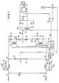
- Fig. 1 depicts a prior art type single-stage inverter (with additional shoot-through protection to be described);
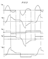
- Fig. 2 depicts idealized current and voltage waveforms, for a zero-impedance load, which will be helpful in understanding the operation of the inverter of Fig. 1;
- Fig. 3 depicts comparable waveforms for a non-zero load;
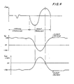
- Fig. 4 depicts what happens in the event of a shoot-through;
- Fig. 5 depicts the illustrative embodiment of the invention;
- Fig. 6 depicts a preferred form of
decoder 27 for use in the system of Fig. 5; and - Fig. 7 depicts a feed-forward circuit whose use in the system of Fig. 5 is advantageous.
- In the system of Fig. 1, which shows a single stage inverter, the DC input is applied across
terminals terminal 10 being at a +150 volt potential andterminal 12 being at a potential of -150 volts. Capacitor 98 is typically very large in magnitude, e.g. 5,000 microfarads. An electrolytic capacitor is employed, to minimize the volume of the overall system.Capacitor 98 can be thought of as part of the DC input power source. It serves to smooth the input in the event it is derived from an AC line, and it is not essential to the inverter operation. - The inverter includes two series circuits, each having an
SCR Control circuit 34 alternately triggers the two SCRS throughpulse transformers capacitor 46 and a load. The actual circuitry depicted for the load in Fig. 1 is one which is often found in practice. The inverter functions to transform the DC input potential to an AC potential across a load. In a typical application, however, what is desired is a DC potential. Thus what is shown in Fig. 1 is a standard rectifier which includes atransformer 48, a pair ofdiodes 50 and afilter capacitor 52, together with a "real"load 56. - In order to control the amplitude of the DC output potential, a feedback circuit is employed.
Resistors difference amplifier 60. Areference potential 64 is extended through avariable potentiometer 62 to the minus input of the difference amplifier. The amplifier output is thus an indication of the difference between the actual DC potential derived and that which is desired. The output of the amplifier is extended to the input ofcontrol circuit 34. The control circuit is simply a voltage-to-frequency converter which alternatelypulses transformers control line 36. The voltage-to-frequency converter ofcontrol circuit 34 provides a polarity reversal so that an increase in voltage on thecontrol line 36 causes a corresponding reduction in frequency. This standard type of feedback circuit causes the SCRs to be fired more frequently when the DC output potential must be increased, and less frequently when the DC output potential must be decreased. Control and feedback circuits for inverter systems are well known in the art, and any of many standard circuits may be employed. - The system operation can be best understood by assuming that resonating
capacitor 46 is initially discharged, that no current flows in the circuit, and that the load (betweencapacitor 46 and the junction ofcapacitor 70,72) is replaced by a short circuit. In such a case,nodes SCR 18 is fired, a 150-volt potential appears acrossinductor 42,capacitor 46 and the load. Typically,capacitors e.g. capacitor 46 may be only 1 microfarad), so the effect ofcapacitors terminal 10 andnode 24 as constituting a zero-impedance power supply). Current starts to flow down throughinductor 42, to the right throughcapacitor 46, and down through the load. Even if the load has zero impedance, as assumed, the peak current is limited by the resonantcircuit comprising inductor 42 andcapacitor 46, the peak current being proportional to the product of the DC input voltage and the square root of the ratio of the magnitudes ofcapacitor 46 andinductor 42, as is known in the art. Because the inductor and the capacitor comprise a resonant circuit, the current reverses direction after one-half cycle. As soon as the current reverses direction,SCR 18 turns off. The current which now flows upward throughinductor 42 flows throughcommutating diode 38. In the case of a zero-impedance load, the negative current peak has the same magnitude as the positive current peak. At the end of the second half-cycle,diode 38 ceases to conduct. Current flow ceases altogether because positive current (down through inductor 42) can flow only whenSCR 18 is on, and it is not fired again. One of the main advantages of the use of a resonant circuit in this manner is that current flow always ceases at the end of a cycle of the oscillatory waveform when the current is zero. Were the current to otherwise cease abruptly, large transient voltages would be induced and the resulting radiation might interfere with connected electronic equipment. - With a zero-impedance load, the potential at
node 22 after the first half-cycle is 300 volts, and the potential at the end of the overall cycle is one again zero. In a practical situation, of course, the load does have impedance. Also, at the end of a cycle when the current has returned to zero, the voltage acrosscapacitor 46 will not be zero, and the capacitor remains charged. WereSCR 18 the only switching device employed, each firing of it would increase the charge oncapacitor 46, and after several cycles of operation the capacitor would be charged to the point at which no more power could be delivered through it to the load. In order to restore the charge acrosscapacitor 46,SCR 20 is employed. Each time that this device is fired, it causes a current to flow in the reverse direction through the capacitor, thus giving rise to an AC potential across the output transformer. Assuming a short-circuited load, however, the current throughcapacitor 46 and the voltage atnode 22 are both zero at the end of a single cycle of resonance through the series circuit which includesSCR 20. - Fig. 2 depicts several current and voltage waveforms for the case of a short-circuited load. The first waveform represents the current through
capacitor 46, with positive current being in the left-to-right direction and with the peak currents typically being about 50 amperes and -50 amperes respectively. At time 3a,SCR 18 is fired and a resonating current starts to flow through the SCR,inductor 42 andcapacitor 46. The current reaches a peak of 50 amperes when the supply potential of 150 volts appears at node 22 (the second waveform of Fig. 2). The current then starts to decrease and goes to zero at time 3b, with the potential atnode 22 rising to. 300 volts and the SCR turning off. During the second half-cycle diode 38 conducts, a negative current flows, and the voltage atnode 22 returns to zero. At time 3c, current stops flowing and the voltage atnode 22 remains at zero. - Some time later, at
time 3d,SCR 20 is triggered. Now current first flows from right to left through the capacitor. Attime 3e,SCR 20 turns off and the voltage atnode 22 is at -300 volts. Diode 40 conducts during the second half-cycle, all current flow ceasing attime 3f. - The third waveform on Fig. 2 depicts the voltage at
node 27. For as long as current flows throughinductor 12,SCR 18 ordiode 30 conducts andnode 27 is held at the 150-volt potential atterminal 10. When bothSCR 18 anddiode 38 are off, the potential atnode 27 simply tracks that atnode 22. Similar remarks apply to the fourth waveform of Fig. 2 which depicts the voltage atnode 29. - The analysis above for the case of a zero-impedance load always applies insofar as the cessation of current flow is concerned at the end of each cycle of operation, but it is not true in the case of a real load that the potential across
capacitor 46 is zero at the end of each cycle. There are therefore abrupt steps in voltage at node 22 (and therefore atnodes 27 and 29), and the capacitor current is lower in magnitude when the commutating diodes conduct than when the SCRs conduct. However, while the polarity of the charge on the capacitor is reversed between alternate cycles, a degree of symmetry is maintained in that at the beginning of each cycle the magnitude of the starting voltage across the capacitor is always the same, and the net DC current through the capacitor is zero. Fig. 3 depicts four waveforms comparable to those of Fig. 2 for a non-zero load, one which results in a voltage waveform at node 33 (across the primary winding of transformer 48) which alternates between +100 and -100 volts. The waveform atnode 33 is also shown in Fig. 3. - As mentioned above, one of the main advantages of the prior art type circuit of Fig. 1 is that whenever an SCR is fired, the resulting current constitutes only a single cycle of an oscillatory waveform, the current flowing through the SCR during-the first-half-cycle and through the respective commutating diode during the second half-cycle. The SCR turns off automatically when the current drops below the "holding" value, the diode turns off at the end of the cycle when the current attempts to reverse direction once again, and there is no second cycle of conduction because the SCR remains off. The rate at which the SCRs are fired determines the total power delivered to the load, and thus a simple voltage-to-frequency control circuit can be employed to vary the output potential across the load.
- The system of Fig. 1 is provided with protection against simultaneous conduction of the SCRs, a condition known as shoot-through and which might otherwise damage the SCRs and result in shut down of the power supply.
-
Capacitors SCRs capacitors inductors chokes Capacitors inductors - Typically,
capacitor 46 has a magnitude of one microfarad. The peak current which is reached when inductor 42 (or inductor 44) resonates withcapacitor 46 is proportional to the square root of the ratio of the capacitance ofcapacitor 46 to the inductance ofinductor 42. Similarly, the peak current which is achieved whencapacitors inductors capacitors capacitor 46, the peak current which is reached following a shoot-through is equal to about 4.5 (the square root of 20) times the peak current which is reached during normal operation, that is, the peak repetitive current which flows during normal inverter cycling. A typical SCR can absorb a single pulse whose peak is about ten times its normal maximum repetitive current; consequently, the single large pulse which flows through the two SCRs during the first half-cycle of the resonating current which follows a shoot-through can be absorbed without damaging the SCRs-provided that the pulses occur at a low enough repetition rate (e.g., 10 Hz). - As current flows through the resonant
circuit comprising capacitors inductors capacitors node 41 being at -150 volts andnode 43 being at +150 volts. Until the SCRs turn off,diodes 38 and 40 are short-circuited and no currents flow through them. But as soon as the SCRs turn off, current reverses in the resonant circuit,diodes 38 and 40 now conducting reverse currents. The voltage atnode 41 now starts to rise from -150 volts. Even after the potential passes through zero,diode 38 continues to conduct current which is being forced to flow byinductor 42. Were the potential atnode 41 allowed to continue to rise until the end of the negative half-cycle, the potential could rise well above +150 volts, depending upon when the shoot-through occurs and the values ofinductors 82, 84 (which acquire energy during the shoot-through when large voltages exist across the inductors). At the end of the negative half-cycle of resonance, current would cease to flow throughdiode 38, but the diode might now be reverse biased by a potential much higher than the nominal potential betweenterminal 10 andcommon node 22. The large positive potential atnode 41 might stressSCR 18 anddiode 38 if normal triggering continued throughout the shoot-through period. On the other hand, ifSCR 18 anddiode 38 are both off,capacitor 70 resonates withinductor 82.Inductor 82 must be large in magnitude (e.g., 200 microhenries), that is, many times larger in magnitude thaninductor 42, in order to isolate the DC input power source fromcapacitors - It is for these reasons that the clamping circuits are provided. As the potential at
node 41 rises to a level slightly about +150 volts,diode 94 conducts. It is at this time during the reverse half-cycle that current flows throughdiode 94 to chargecapacitor 90 and to limit the voltage developed acrossinductor 82. By thetime diode 94 turns off, there is still some energy stored in the inductor, and it is only now thatcapacitor 70 starts to resonate withinductor 82. While the resonance would ordinarily persist for quite some time due to the high. inductance ofinductor 82, there is relatively little energy remaining to be dissipated. Consequently,control circuit 34 can immediately begin to control a resumption of normal operation. Similar remarks apply to the clamping circuit associated withinductor 84 and the negative potential which would otherwise develop atnode 43. - Fig:"4 depicts three waveforms which illustrate the operation when a shoot-through occurs. The first waveform depicts the current through
inductor 44. At the left of the wavefarm is the current which flows during normal operation, this current being the same as the middle current cycle at the top of Fig. 3 (since the same current flows throughcapacitor 46 and inductor 44). The waveforms of Fig. 4 are drawn to a much lower scale than those of Fig. 3. It is to be noted that when a shoot-through takes place, large currents flow throughinductor 44, the peaks reaching above +200 and below -200 amperes. - The two lower waveforms in Fig. 4 depict the voltages at
nodes inductors capacitor 46 during normal operation. But when a shoot-through occurs, the voltages atnodes capacitors - When a shoot-through is present,
node 43 rises in potential well above the potential atnode 24. At this time one-shot multivibrator 80 is triggered. The output of the multivibrator is applied to an inhibit input ofcontrol circuit 34, the control circuit thus being disabled and no longer applying triggering pulses to the SCRs. The period of the multivibrator should be selected in accordance with the particular application. For example, if it is known that when arcing occurs it will be continuous for quite some time, the control circuit should be inhibited for at least this duration. However, in many applications the control circuit needs to be inhibited for a period of perhaps only 200 microseconds to 20 milliseconds. Recovery from the shoot-through fault allows normal inverter operation to resume almost immediately without requiring any manual intervention such as operating a circuit breaker. - The problem with the prior art circuit of Fig. 1 is the wide range of frequencies required to cover output voltage and current variations from zero to full specified values. The circuit of Fig. 5 (in which components comparable to those in Fig. 1 have the same numeral designations) overcomes this problem by switching in combinations of inverters so that the operating frequency remains high (above the audio range) at all power levels. In addition to providing this advantage, the circuit allows much higher maximum output power to be obtained than is possible with just one inverter.
- Input power from a nominal 220V AC source at terminals 11 is rectified by bridge 13 to develop a 300-volt potential across
capacitor 98. Separate high-frequency filter capacitors 70-1 through 72-4 (comparable tocapacitors node - The circuit of Fig. 5 is in many respects similar to that of Fig. 1. The main differences relates to the control section, and to the incorporation of four inverter stages ST-1 through ST-4 connected in parallel. Gates and
drivers 21 trigger respective stages in a manner comparable to that in which the individual stage of Fig. 1 is triggered. (Terminals 35-2 through 37-4 are connected to respective terminals 29-2 through 31-4 in a manner equivalent to that shown for stage ST-1) Thecircuit 21 simply extends pulses from the voltage-to-frequency converter 19 to a number of pulse transformers 30-1 through 32-4 in accordance with the count ofcounter 25. For example, if the count is binary 1010, only the pulse transformers associated with stages ST-2 and ST-4 will be pulsed. - The four resonant circuits are connected in parallel so that the inverter stage currents can be summed together. Because the resonant frequency of a stage is proportional to the product of its inductor (42- or 44-) and capacitor (46-), all stages operate at the same frequency; while the capacitors of successive stages are doubled in magnitude, the inductor magnitudes are halved. At the same time, however, successive stages provide doubled increments of power because the power delivered by any stage is proportional to the square root of its capacitance divided by its inductance. Inverter stage ST-1 provides a maximum of 1/15 of the total power capability of the complete inverter system. In reality, the useful output power available from this section is usually much less than 1/15 of the total since fixed circuit losses, particularly when a step-up transformer ratio is used, can absorb a significant part of the power available from this least significant power stage. The result is a high frequency of operation, even at low output voltages and current levels. In addition, a pre-load of typically 3% to 5% is often used to provide discharge in the output circuit and a fast response under light load conditions. The least significant stage therefore provides power for the losses in the system, leaving only a very small percentage (typically less than 2% of the maximum output power) for useful output power, even when running at maximum frequency (e.g., 40 KHz). The frequency at which this stage operates is above the audio range at all usable power levels. At extremely low levels (e.g., less than 1% of output power), the inverter frequency could fall into the audio range, but at these power levels the noise from the magnetic components is insignificant, and ripple requirements are less critical.
- At all other power levels, operation remains above audio (20 KHz), as will now be described.
- The basic control circuit comprises a voltage-to-
frequency converter 19 which drives the gate electrodes of the SCRs in the four inverter stages ST-1 through ST-4 via logic gates anddriver circuits 21. These logic circuits determine which SCRs receive the gate drive pulses generated from the outputs of the voltage-to-frequency converter 19. Control for the logic gates is derived from the input signal to the voltage-to-frequency converter which is an inverse voltage representation of the frequency, and hence the power, of the inverter stages in use at any instant. - This input voltage is inverted by
inverter 61. The inverted voltage is applied tovoltage comparator 23 which determines a voltage "window" used for triggering up/downcounter 25. As the frequency of the inverter approaches maximum due to increased power required at the load, the control voltage at the input of the comparator approaches the high limit trip level determined byvoltage source 55 and potentiometer 57. When the trip point is reached, the inverter frequency has reached the maximum design limit (e.g. 40 kHz), and a pulse is then sent to the up/down counter to step up the digital counter. The outputs from the up/down counter gate on the appropriate combination of SCRs in the inverter stages to produce additional power, in this case equal to that of the lowest power stage. As a result of this increase in inverter power, the output voltage (or current) tends to rise. This is sensed by the feedback signal which is compared with the reference potential bycontrol amplifier 60, and results in a compensating change in voltage applied to the voltage-to-frequency converter andcomparator 23. The frequency of the inverter is thereby reduced and the voltage applied to the comparator returns to within the normal operating window. - Similarly, when the output power requirements are reduced, the inverter frequency is lowered by the signal from
amplifier 60, and the voltage at the input ofcomparator 23 approaches the low trip level. At the trip point, the comparator sends a down control pulse to the up/down counter, reducing the digital counter by unity. This gates the drive to the appropriate combination of inverters so that the available output power is reduced by an amount equal to that of the lowest power stage (least significant bit). The output voltage then tends to fall, and the feedback signal causes a control voltage to be applied to the voltage-to-frequency converter 19 so as to increase the frequency and bring the input voltage to the comparator back within the normal operating window. - With this logic arrangement, the low trip level of
comparator 23 should change with the count in the up/down counter since the frequency change with each bit change varies from 2:1 for the lowest bit to 1.07:1 for the highest bit. This is achieved bydecoder 27 which decodes the output of the up/down counter, and changes the low trip ievel of the comparator so that it tracks the count in the up/down counter. - Consider the case in which all four stages are delivering current to the load and the upper frequency limit is 40 kHz. As the load requirements decrease, the frequency decreases. Eventually the frequency decreases to a value such that the stage which delivers the lowest value current should be disabled from operating. If the stage is disabled at this time, the remaining three stages will have to operate at a faster rate in order to satisfy the load requirement. If this rate is 40 kHz or more, the system will be unstable and will flip back to its original condition in which all four stages are enabled.
- For this reason, the lower frequency limit which is used for any combination of enabled stages is a value which corresponds to a power level less than that which would otherwise be required to restore the frequency back to 40 kHz when the count of
counter 25 is decremented. By doing this, when the least significant stage is switched out, the operating frequency will increase to a value less than the upper limit, e.g., 38 kHz. It should also be appreciated that as the total power is reduced, the lower frequency limit is reduced in larger and larger increments. The reason for this is that at the lower power levels, the percentage effect of a single bit change on the overall power being delivered at the time is greater. This variation in control of the low frequency limit is the function ofdecoder 27 in Fig. 5. The decoder itself is shown in a preferred form in Fig. 6. - The four inputs to
decoder 27 are derived from the up/downcounter 25, and are shown by the dashed lines 140-1 through 140-8. Each of the counter outputs controls the operation of a gate 142-1 through 142-8, each gate being shown in symbolic form only. For example, when the second least significant bit of the counter is a 1, and stage ST-2 in Fig. 5 is enabled to deliver current, switch 142-2 is open. The switch is closed only when the corresponding stage is not enabled. Each switch bypasses a respective one ofresistors Resistor 137 is a bias resistor which determines the minimum low frequency limit in combination withadjustment potentiometer 139. The resistor chain is connected to the minus input ofoperational amplifier 144, which is provided with afeedback resistor 146 typically equal in value to that ofresistor 136. The net effect of the arrangement is that the output of theoperational amplifier 144, which is a voltage that determines the low frequency limit ofcomparator 23, varies in accordance with the particular group of stages ST-1 through ST-4 whose operations are enabled. - Improvements in smoothing the small step in the output voltage during a bit change can be made by decoding the outputs of the up/down counter and applying the decoded output voltage to the input of the voltage-to-frequency converter so as to provide a feed-forward signal while the main control loop takes control. Referring to Fig. 5, it will be noted that as the feedback signal from the load increases, the output of
operational amplifier 60 increases. Because an increasing feedback signal represents a need to reduce the power level, voltage-to-frequency converter 19 operates so that its frequency of operation decreases as its input voltage increases. Referring to Fig. 7, a feed-forward signal circuit is provided which tends to speed up the change in the frequency of operation immediately following a change in the group of stages which are enabled.Operational amplifier 60 is shown on Fig. 7 together with voltage-to-frequency converter 19. Between the output ofamplifier 60 and the input ofconverter 19, there are two inversion stages which compriseoperational amplifiers amplifier 60 on the voltage-to-frequency converter 19 is thus the same in Fig. 7 as it is in Fig. 5. It is the additional circuitry on Fig. 7 which controls a rapid change in the frequency of operation following a change in the group of inverter stages whose operations are enabled. - The reason for providing the feed-forward circuit is that following a change in the group of stages whose operations are enabled, it takes some time until the feedback circuit causes a change in the operating frequency. During this transitional period, there may be exhibited a power variation at the output. In order to avoid this, a rapid change in the operating frequency is effected.
- The change is effected by providing an additional operational amplifier 108 (with
feedback resistor 109 and isolating resistor 110), together with a resistor chain and associated gates whose operations are controlled by the bit outputs of the up/downcounter 25. The resistor chain connected to the minus input ofoperational amplifier 108 is comparable to the resistor chain shown in Fig. 6. Whenever there is a change in the group of inverter stages whose operations are enabled, there is a sudden change in the potential of the output ofoperational amplifier 108, and thus a rapid change in the frequency of operation. At the lower power levels, this change is larger than at higher power levels. The resistor magnitudes are selected such that the instantaneous frequency change in each case just cancels out any power level change which might otherwise occur due to the switching of the stages. - The type of logic, method of control and the number of SCR inverter stages are variables that depend upon the application of the power supply. However, these variables do not affect the basic principles of the invention which requires a multiple number of inverter power stages that are switched in as required by the load to keep the inverter frequency high under all loading conditions, and a fine adjustment of frequency to provide precise control of output power at all power levels.
Claims (7)
Priority Applications (1)
| Application Number | Priority Date | Filing Date | Title |
|---|---|---|---|
| AT83903659T ATE31852T1 (en) | 1982-11-15 | 1983-10-07 | POWER SUPPLY WITH DC INPUT SOURCE AND PULSED POWER SUPPLY LEVELS. |
Applications Claiming Priority (2)
| Application Number | Priority Date | Filing Date | Title |
|---|---|---|---|
| US06/441,660 US4488214A (en) | 1982-11-15 | 1982-11-15 | High-power, high-frequency inverter system with combined digital and analog control |
| US441660 | 1982-11-15 |
Publications (3)
| Publication Number | Publication Date |
|---|---|
| EP0125278A1 EP0125278A1 (en) | 1984-11-21 |
| EP0125278A4 EP0125278A4 (en) | 1985-07-30 |
| EP0125278B1 true EP0125278B1 (en) | 1988-01-07 |
Family
ID=23753773
Family Applications (1)
| Application Number | Title | Priority Date | Filing Date |
|---|---|---|---|
| EP83903659A Expired EP0125278B1 (en) | 1982-11-15 | 1983-10-07 | Power supply having a dc imput power source and pulsed current supplying stages |
Country Status (6)
| Country | Link |
|---|---|
| US (1) | US4488214A (en) |
| EP (1) | EP0125278B1 (en) |
| JP (1) | JPH0655034B2 (en) |
| CA (1) | CA1206198A (en) |
| DE (1) | DE3375262D1 (en) |
| WO (1) | WO1984002041A1 (en) |
Families Citing this family (15)
| Publication number | Priority date | Publication date | Assignee | Title |
|---|---|---|---|---|
| US4695933A (en) * | 1985-02-11 | 1987-09-22 | Sundstrand Corporation | Multiphase DC-DC series-resonant converter |
| DE3671343D1 (en) * | 1985-07-26 | 1990-06-21 | Bbc Brown Boveri & Cie | VOLTAGE INVERTER. |
| US4805081A (en) * | 1987-06-29 | 1989-02-14 | Spellman High Voltage Electronics Corp. | Multi-mode control systems for high-frequency resonant inverters |
| US4823250A (en) * | 1987-11-05 | 1989-04-18 | Picker International, Inc. | Electronic control for light weight, portable x-ray system |
| JP2707465B2 (en) * | 1989-06-29 | 1998-01-28 | スタンレー電気株式会社 | Inverter device |
| DE69030847T2 (en) * | 1989-07-31 | 1997-09-18 | Fuji Photo Film Co Ltd | Process for processing silver halide color photographic material |
| US5146395A (en) * | 1991-08-09 | 1992-09-08 | Mckie Richard L | Power supply including two tank circuits |
| US5324990A (en) * | 1992-04-03 | 1994-06-28 | Cunningham John C | Voltage inverter power conservation circuit |
| US5414238A (en) * | 1992-10-02 | 1995-05-09 | Martin Marietta Corporation | Resonant power supply for an arcjet thruster |
| US5602897A (en) * | 1995-06-29 | 1997-02-11 | Picker International, Inc. | High-voltage power supply for x-ray tubes |
| US5671132A (en) * | 1996-03-13 | 1997-09-23 | Spellman High Voltage Company | High voltage bipolar CT scanner power supply |
| US6946824B2 (en) * | 2001-09-06 | 2005-09-20 | Intel Corporation | Power delivery system having a plurality of stages and method for setting power delivery system parameters |
| FR2834392A1 (en) * | 2001-12-28 | 2003-07-04 | St Microelectronics Sa | HIGH VOLTAGE OSCILLATOR HAVING FAST REACTION TIME |
| US8360977B2 (en) * | 2007-09-27 | 2013-01-29 | Baxter International Inc. | Continuity circuits for detecting access disconnection |
| US7948222B2 (en) | 2009-02-05 | 2011-05-24 | Advanced Micro Devices, Inc. | Asymmetric topology to boost low load efficiency in multi-phase switch-mode power conversion |
Citations (1)
| Publication number | Priority date | Publication date | Assignee | Title |
|---|---|---|---|---|
| US3823262A (en) * | 1972-10-24 | 1974-07-09 | Coloroptics Inc | Facsimile recorder with compensation of the electrosensitive blank nonlinear applied voltage-burn characteristic |
Family Cites Families (4)
| Publication number | Priority date | Publication date | Assignee | Title |
|---|---|---|---|---|
| DE2221200A1 (en) * | 1972-04-29 | 1973-11-08 | Licentia Gmbh | ASTABLE PULSE GENERATOR FOR GENERATING BIPOLAR PULSES |
| US3823362A (en) * | 1973-02-02 | 1974-07-09 | Gen Electric | Coordinated master-slave converter system for variable-power tank loads |
| JPS5280427A (en) * | 1975-12-26 | 1977-07-06 | Mitsui Shipbuilding Eng | Method of controlling time division type inverter |
| JPS5840916B2 (en) * | 1978-11-13 | 1983-09-08 | 日本電信電話株式会社 | Natural commutation type DC↓-DC converter |
-
1982
- 1982-11-15 US US06/441,660 patent/US4488214A/en not_active Expired - Lifetime
-
1983
- 1983-10-07 JP JP58503588A patent/JPH0655034B2/en not_active Expired - Fee Related
- 1983-10-07 WO PCT/US1983/001577 patent/WO1984002041A1/en active IP Right Grant
- 1983-10-07 EP EP83903659A patent/EP0125278B1/en not_active Expired
- 1983-10-07 DE DE8383903659T patent/DE3375262D1/en not_active Expired
- 1983-10-28 CA CA000439987A patent/CA1206198A/en not_active Expired
Patent Citations (1)
| Publication number | Priority date | Publication date | Assignee | Title |
|---|---|---|---|---|
| US3823262A (en) * | 1972-10-24 | 1974-07-09 | Coloroptics Inc | Facsimile recorder with compensation of the electrosensitive blank nonlinear applied voltage-burn characteristic |
Also Published As
| Publication number | Publication date |
|---|---|
| EP0125278A4 (en) | 1985-07-30 |
| CA1206198A (en) | 1986-06-17 |
| JPS59502051A (en) | 1984-12-06 |
| JPH0655034B2 (en) | 1994-07-20 |
| WO1984002041A1 (en) | 1984-05-24 |
| US4488214A (en) | 1984-12-11 |
| DE3375262D1 (en) | 1988-02-11 |
| EP0125278A1 (en) | 1984-11-21 |
Similar Documents
| Publication | Publication Date | Title |
|---|---|---|
| EP0125278B1 (en) | Power supply having a dc imput power source and pulsed current supplying stages | |
| US4523269A (en) | Series resonance charge transfer regulation method and apparatus | |
| US5629844A (en) | High voltage power supply having multiple high voltage generators | |
| US4686615A (en) | Power supply circuit | |
| US4493017A (en) | Single drive transformer with regenerative winding for p.w.m. supply having alternately conducting power devices | |
| JP2583258B2 (en) | Method and apparatus for electrostatic power conversion | |
| US4967333A (en) | Stabilized power supply with reduced ripple factor | |
| US5121314A (en) | Bi-mode high voltage resonant power supply and method | |
| US4805081A (en) | Multi-mode control systems for high-frequency resonant inverters | |
| EP0107313B1 (en) | Resonant current-driven power source | |
| JPS61158698A (en) | Inverter-type x-ray plant | |
| EP0391617B1 (en) | Method and network for enhancing power factor of off-line switching circuit | |
| US4055791A (en) | Self commutated SCR power supply | |
| CA1163677A (en) | Method and apparatus for controlling a resonant power module | |
| JPH0232757A (en) | Inductive power converter for application with variable input/output voltage | |
| CA1318349C (en) | Series resonant power converter and method of controlling the same | |
| US4514795A (en) | High-voltage generator, notably for an X-ray tube | |
| US4253139A (en) | Power conversion and regulation system | |
| US5680301A (en) | Series/parallel resonant converter | |
| JPH0622551A (en) | Resonance-type dc-dc converter | |
| US3881146A (en) | Self-commutating flux-gated inverter | |
| JPH08130871A (en) | Dc-dc converter | |
| CA1192258A (en) | Variable single phase inverter | |
| AU2208783A (en) | High-power, high-frequency inverter system with combined digital and analog control | |
| EP0253432B1 (en) | Energy converter |
Legal Events
| Date | Code | Title | Description |
|---|---|---|---|
| PUAI | Public reference made under article 153(3) epc to a published international application that has entered the european phase |
Free format text: ORIGINAL CODE: 0009012 |
|
| AK | Designated contracting states |
Designated state(s): AT BE CH DE FR GB LI LU NL SE |
|
| 17P | Request for examination filed |
Effective date: 19841102 |
|
| 17Q | First examination report despatched |
Effective date: 19860512 |
|
| GRAA | (expected) grant |
Free format text: ORIGINAL CODE: 0009210 |
|
| AK | Designated contracting states |
Kind code of ref document: B1 Designated state(s): AT BE CH DE FR GB LI LU NL SE |
|
| PG25 | Lapsed in a contracting state [announced via postgrant information from national office to epo] |
Ref country code: LI Effective date: 19880107 Ref country code: CH Effective date: 19880107 Ref country code: BE Effective date: 19880107 Ref country code: AT Effective date: 19880107 |
|
| REF | Corresponds to: |
Ref document number: 31852 Country of ref document: AT Date of ref document: 19880115 Kind code of ref document: T |
|
| PG25 | Lapsed in a contracting state [announced via postgrant information from national office to epo] |
Ref country code: SE Effective date: 19880131 |
|
| REF | Corresponds to: |
Ref document number: 3375262 Country of ref document: DE Date of ref document: 19880211 |
|
| ET | Fr: translation filed | ||
| REG | Reference to a national code |
Ref country code: CH Ref legal event code: PL |
|
| PG25 | Lapsed in a contracting state [announced via postgrant information from national office to epo] |
Ref country code: LU Free format text: LAPSE BECAUSE OF NON-PAYMENT OF DUE FEES Effective date: 19881031 |
|
| PLBE | No opposition filed within time limit |
Free format text: ORIGINAL CODE: 0009261 |
|
| STAA | Information on the status of an ep patent application or granted ep patent |
Free format text: STATUS: NO OPPOSITION FILED WITHIN TIME LIMIT |
|
| 26N | No opposition filed | ||
| REG | Reference to a national code |
Ref country code: GB Ref legal event code: IF02 |
|
| PGFP | Annual fee paid to national office [announced via postgrant information from national office to epo] |
Ref country code: GB Payment date: 20021002 Year of fee payment: 20 |
|
| PGFP | Annual fee paid to national office [announced via postgrant information from national office to epo] |
Ref country code: FR Payment date: 20021008 Year of fee payment: 20 |
|
| PGFP | Annual fee paid to national office [announced via postgrant information from national office to epo] |
Ref country code: DE Payment date: 20021011 Year of fee payment: 20 |
|
| PGFP | Annual fee paid to national office [announced via postgrant information from national office to epo] |
Ref country code: NL Payment date: 20021031 Year of fee payment: 20 |
|
| PG25 | Lapsed in a contracting state [announced via postgrant information from national office to epo] |
Ref country code: GB Free format text: LAPSE BECAUSE OF EXPIRATION OF PROTECTION Effective date: 20031006 |
|
| PG25 | Lapsed in a contracting state [announced via postgrant information from national office to epo] |
Ref country code: NL Free format text: LAPSE BECAUSE OF EXPIRATION OF PROTECTION Effective date: 20031007 |
|
| REG | Reference to a national code |
Ref country code: GB Ref legal event code: PE20 |
|
| NLV7 | Nl: ceased due to reaching the maximum lifetime of a patent |
Effective date: 20031007 |