EP0123370A1 - Electro-optical imaging system with diagnostic facility - Google Patents
Electro-optical imaging system with diagnostic facility Download PDFInfo
- Publication number
- EP0123370A1 EP0123370A1 EP84300433A EP84300433A EP0123370A1 EP 0123370 A1 EP0123370 A1 EP 0123370A1 EP 84300433 A EP84300433 A EP 84300433A EP 84300433 A EP84300433 A EP 84300433A EP 0123370 A1 EP0123370 A1 EP 0123370A1
- Authority
- EP
- European Patent Office
- Prior art keywords
- lamp
- during
- electro
- array
- signal
- Prior art date
- Legal status (The legal status is an assumption and is not a legal conclusion. Google has not performed a legal analysis and makes no representation as to the accuracy of the status listed.)
- Granted
Links
Images


Classifications
-
- H—ELECTRICITY
- H04—ELECTRIC COMMUNICATION TECHNIQUE
- H04N—PICTORIAL COMMUNICATION, e.g. TELEVISION
- H04N1/00—Scanning, transmission or reproduction of documents or the like, e.g. facsimile transmission; Details thereof
- H04N1/00002—Diagnosis, testing or measuring; Detecting, analysing or monitoring not otherwise provided for
- H04N1/00007—Diagnosis, testing or measuring; Detecting, analysing or monitoring not otherwise provided for relating to particular apparatus or devices
- H04N1/00013—Reading apparatus
-
- H—ELECTRICITY
- H04—ELECTRIC COMMUNICATION TECHNIQUE
- H04N—PICTORIAL COMMUNICATION, e.g. TELEVISION
- H04N1/00—Scanning, transmission or reproduction of documents or the like, e.g. facsimile transmission; Details thereof
- H04N1/00002—Diagnosis, testing or measuring; Detecting, analysing or monitoring not otherwise provided for
- H04N1/00026—Methods therefor
- H04N1/00029—Diagnosis, i.e. identifying a problem by comparison with a normal state
-
- H—ELECTRICITY
- H04—ELECTRIC COMMUNICATION TECHNIQUE
- H04N—PICTORIAL COMMUNICATION, e.g. TELEVISION
- H04N1/00—Scanning, transmission or reproduction of documents or the like, e.g. facsimile transmission; Details thereof
- H04N1/00002—Diagnosis, testing or measuring; Detecting, analysing or monitoring not otherwise provided for
- H04N1/00026—Methods therefor
- H04N1/00053—Methods therefor out of service, i.e. outside of normal operation
-
- H—ELECTRICITY
- H04—ELECTRIC COMMUNICATION TECHNIQUE
- H04N—PICTORIAL COMMUNICATION, e.g. TELEVISION
- H04N1/00—Scanning, transmission or reproduction of documents or the like, e.g. facsimile transmission; Details thereof
- H04N1/00002—Diagnosis, testing or measuring; Detecting, analysing or monitoring not otherwise provided for
- H04N1/00026—Methods therefor
- H04N1/00063—Methods therefor using at least a part of the apparatus itself, e.g. self-testing
-
- H—ELECTRICITY
- H04—ELECTRIC COMMUNICATION TECHNIQUE
- H04N—PICTORIAL COMMUNICATION, e.g. TELEVISION
- H04N1/00—Scanning, transmission or reproduction of documents or the like, e.g. facsimile transmission; Details thereof
- H04N1/0035—User-machine interface; Control console
- H04N1/00405—Output means
- H04N1/0049—Output means providing a visual indication to the user, e.g. using a lamp
Definitions
- This invention relates to electro-optical imaging systems of the kind including: a reference background adapted to reflect radiant energy impinging thereon; illuminating means adapted to illuminate said reference background during an on mode of operation; scanning means including at least one array having N photosensitive elements adapted to provide N reference pixed signals for each scan of said reference background; and error signal generating means including comparison means adapted to produce an error signal whenever any reference pixel signal is less than a predetermined reference level.
- An electro-optical imaging system of the kind specified is known from U.S. Patent Specification No. 4,287,536.
- the known electro-optical imaging system includes a pair of multi-element scanning arrays arranged to scan a calibration strip and thereby provide outputs which are each compared with a preset reference level to develop a corrective signal which controls the gain of each of the arrays.
- the known system also discloses an arrangement wherein the calibration strip is scanned in each of a plurality of modes and the image data output is applied to a microprocessor unit which compares the image signal output with a predetermined minimum voltage level or threshold.
- the comparison output represents the image signal as being above or below the minimum threshold a binary "1” or a binary "0” is loaded into an associated location in a random access memory (RAM).
- RAM random access memory
- the contents of the RAM are utilized such that a stored "0", indicating a "bad” photosensitive element, causes the previous pixel signal to be substituted for the "bad” pixel signal.
- the failure of a photosensitive element may be indicative of an impending partial or total failure of the photosensitive array. A problem experienced with the known system that unacceptable system outputs may be produced resulting from such photosensitive array failure.
- an electro-optical imaging system of the kind specified characterized by indicator means adapted to indicate to an operator that at least one of said photosensitive elements in said array is defective.
- a system according to the invention has the advantage that an operator is made aware that one or more photosensitive elements in the array is defective. This gives the operator an early warning indication of a possible impending failure of the array. With such an indication, the operator would have an opportunity to arrange for the array to be serviced by repair or replacement in time before any partial or total failure of the array actually occurs.
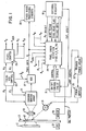
- FIG. 1 discloses a schematic block diagram of a preferred embodiment of the invention.
- the invention is shown in a video camera environment or application for scanning information from objects or documents.
- a reference background 11 which is preferably white in color, is mounted near or adjacentto a moving track or moving conveyor line or mounted on a rotating drum 13.
- the reference background is illuminated by radiant energy, such as by light from a suitable light source or lamp 15.
- An object or document 17 to be imaged can be either stationary or transported by the moving track, moving conveyor line or rotating drum 13 along a path between the reference background 11 and a lens assembly 19. As the object 17 is moved across the reference background, it is illuminated by the light source 15. A reflected optical image of the object 17 is focused by the lens assembly 19 onto the face of an imaging sensor array 21.
- the imaging sensor array 21 could comprise any suitable array such as, for example, an array of photodiodes, a photoarray or a charge coupled device (CCD) array.
- the array 21 is 1024-element CCD array such as, for example, a Model 133/143 CCD, manufactured by CCD Imaging Products Division, Fairchild Camera & Instrument Corporation.
- Transport clocks ⁇ X and transfer clocks 0 T from a timing and control circuit 23 enable the imaging sensor array 21 to generate a plurality of scan lines of an object 17 as the object traverses the scan position of the array 21.
- Each scan line of the array 21 develops 1024 picture elements or pixels, with each pixel having a particular one of 64 gray scale values, which value represents a portion of the object 17 being scanned.
- the composite of these scan lines of the object provides a signal image of the object 17 being scanned.
- Transport clocks ⁇ X control the readout rate of video data from the 1024 cells in the imaging sensor array 21 at a rate of approximately 270 nanoseconds per pixel.
- a transfer clock ⁇ T occurs at the end of each line scan and controls the integration time of the array 21. This so-called integration time of the array 21 is analogous to the exposure time in conventional cameras.
- the scan interval or interpulse period of the transfer clock ⁇ T is approximately 285 microseconds.
- Each transport clock ⁇ X increments an 11-bit, synchronous, binary pixel counter 25 by one, causing its output to sequentially develop address counts or addresses from 0 to 1063.
- the pixel clocks ⁇ X which occur between- the addresses 0 through 1023 are used to sequentially clock out video pixel signals from the 1024 cells or elements 0 through 1023 of the array 21.
- the pixel clocks 0 x which occur between addresses 1024 through 1062 may be utilized to clock out black and white references inside the array 21 for purposes beyond the scope of this invention.
- the 0 T clock which occurs at the end of a scan and during the pixel count of 1063, is used to synchronously reset the counter 25 to an address count of 0 at the following 0 X clock time in order to start a new line scan of the array 21.
- Counts 0 and 1024 of counter 25 are internally decoded by the counter 25 to develop signals P 0 and P 1024 which respectively represent the first and 1024th transport clocks in each line scan. Although the counter 25 develops an 11-bit output, only the 10 least significant bits AO-A9 are outputted for further utilization by the system.
- each transport clock 0y, or ⁇ X is applied from timing and control circuit 23 to enable an analog-to-digital converter (ADC) circuit 27 to digitize the video pixel signals from the array 21 to produce a corresponding scan of digitized pixels or pixel data for each scan line of the array 21.
- ADC analog-to-digital converter
- the ADC circuit 27 may contain two separate ADCs for respectively digitizing the two channel outputs and, in addition, circuitry for interlacing the two digitized channel outputs into one composite output.
- CCD interlacing techniques which form no part of this invention, are described in detail in U.S. Patent No. 3,911,467.
- Each of the digitized pixels from the ADC circuit 27 has a gray scale value which is six bits wide; Each digitized pixel can have one of the 64 gray scale values ranging from completely black (a digital value of 000000) to completely white (a digital value of111111).
- the scans of pixel data from the ADC circuit 27 may be applied to other video processing circuits 28 where, for example, the digitized image of a scanned object 17 can be conventionally reconstructed along X and Y coordinates, scan line by scan line.
- other video processing circuits 28 further utilization of the pixel data by other video processing circuits 28 is beyond the purview of this invention and, hence, will not be further discussed.
- the invention automatically and repeatedly tests each scan of pixel data from ADC 27 for any defective elements or cells in the imaging sensor array 21 during a "diagnostic operation". In the performance of such tests on the pixel data, the pixel data from ADC 27, the ⁇ X and 9 T clocks from timing and control 27, and the P O and P 1024 signals and AO-A9 addresses from pixel counter 25 are applied to a pixel error detection circuit 29.
- an on/off control circuit 31 is included to initiate an initial diagnostic operation of the system after power is initially applied to the system and to initiate a subsequent diagnostic operation each time it receives an external (ext.) reset signal.
- control circuit 31 Each time that the control circuit 31 initiates a diagnostic operation, it sends control signals to the detection circuit 29 to enable the circuit 29 to sequence through different tests on the pixel data from ADC 27. As long as no object 17 is detected in the track 13, the detection circuit 29 will be enabled by a 1 state obj. present signal to complete a diagnostic operation.
- control circuit 31 Each time that the control circuit 31 initiates a diagnostic operation, it also supplies a lamp control signal to control the operation of a primary power relay 33 to either supply or not supply primary power (not shown) to a power supply 35 as a function of the amplitude of the lamp control signal.
- the lamp control signal has an insufficient amplitude to energize the relay 33.
- the power supply 35 provides no power to the lamp 15 and the lamp 15 is "off".
- the imaging sensor array 21 scans the unilluminated reference background 11 (provided that no object 17 is present in the track 13 during this first mode of operation).
- the control signals from control circuit 31 enable the detection circuit 29 to test the pixel data with the lamp 15 "off”.
- the control circuit 31 changes the amplitude of the lamp control signal to end the first mode of operation and start the second mode of operation.
- the control signal has a sufficient amplitude to energize the relay 33.
- the power supply 35 therefore supplies power to turn "on” the lamp 15.
- the imaging sensor array 21 scans the illuminated reference background 11 (provided that no object 17 is present in the track 13 during this second mode of operation).
- the control signals from control circuit 31 enable the detection circuit 29 to test the pixel data with the lamp 15 "on”.
- this second mode of operation is temporarily interrupted each time that an object 17 to be imaged by the array 21 is detected in the track 13. More specifically, as an object 17 moves down the track 13 toward the reference background 11, it passes between a light emitting diode (LED) 37 and light sensor 39 which are respectively positioned on opposite sides of the track 13. The passage of an object 17 between the elements 37 and 39 interrupts the light path between the LED 37 and sensor 39, causing the sensor 39 to develop a 0 state object (obj.) present signal to temporarily interrupt the operation of the detection circuit 29.
- LED light emitting diode
- the object present signal After a suitable time delay after the trailing edge of the object 17 has cleared the path between the LED 37 and sensor 39, the object present signal returns to a 1 state to enable the detection circuit 29 to again test each line scan of pixel data derived from the reference background 11.
- a suitable delay can be readily determined from the known speed of the track 13 after the object 17 clears the path between the LED 37 and sensor 39.
- This known time delay (not shown) can be readily added to the sensor 39 output.
- External circuitry 41 can be any suitable circuit, such as switches, push buttons, a microprocessor or discrete logic, for selectively generating an external reset pulse, a 0T inhibit signal, a diagnostic clear (diag. clr.) signal and diagnostic read clocks (diag. read clk) to read out any pixel failure information from the detection circuit 29.
- External circuitry 41 can be any suitable circuit, such as switches, push buttons, a microprocessor or discrete logic, for selectively generating an external reset pulse, a 0T inhibit signal, a diagnostic clear (diag. clr.) signal and diagnostic read clocks (diag. read clk) to read out any pixel failure information from the detection circuit 29.
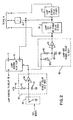
- FIG. 2 illustrates a composite schematic block and circuit diagram of the on/off control circuit 31 of FIG. 1, while FIG. 3 illustrates waveforms useful in explaining the operation of the control circuit 31.
- This low output of buffer 45 is applied to the clear input of a lamp control flip flop 47, which causes the flip flop 47 to develop at its Q output a low level lamp control signal.
- the low level lamp control signal from flip flop 47 turns off the relay 31 which, as indicated in FIG. 1, turns off the power supply 35 and, hence, turns off lamp 15.
- the purpose of the logic stable delay 43 is to provide a delay of approximately one half of a second for the stabilization of the logic power supplies in the system.
- T 1 (FIG.3) after a delay of approximately one half of a second, the charge E C1 on the capacitor C1 has increased to a voltage sufficient to trigger the Schmitt buffer 45 to change its output state from low to high.
- the high output of delay 43 removes the clear signal (0 state) from the lamp control flip flop 47.
- the flip flop 47 is subsequently clocked, it continues to develop a low level lamp control signal.
- the high output of delay 43 is also applied to a lamp off stable delay 49 to provide an additional 1 second delay for the lamp 15 to stabilize in its off state.
- a resistor R2 and capacitor C2 are serially connected to each other between the output of buffer 45 and ground.
- a diode CR1 is connected in parallel to the resistor R2.
- the junction of R2 and C2 is connected to the input of a Schmitt buffer 51.
- capacitor C2 starts charging up toward that high level.
- T 3 (FIG. 3)
- the charge E C2 on the capacitor C2 triggers the Schmitt buffer 51 to change its output state from low to high.
- This output of buffer 51 is the output A of delay 49, as shown in FIG. 3.
- the high level output A of delay 49 is also applied to a 1 second lamp off-to-on stable delay 53, which is similar in structure and operation to the delay 49.
- the output B of delay 53 changes from low to high to clock the lamp control flip flop 47 on its rising edge.
- the lamp control flip flop 47 develops at its Q output a high level lamp control signal which energizes the relay 31, causing power supply 35 to be turned on and to turn on lamp 15.
- the B signal from the output of delay 53 is inverted by a logical inverter 55 to develop a B signal.
- the lamp off pixel error test was conducted for a period of .1 second between times T 3 and T 5 . During this 1 second period of time, approximately 3500 separate scan lines of pixel data could have been tested for pixel errors after the lamp 15 was turned off and stabilized (provided that no object 17 was detected in the track 13 during this time).
- the purpose of the lamp off-to-on stable delay 53 is to provide a delay of approximately 1 second for the lamp 15 to stabilize in its on state before any lamp on pixel error tests are conducted by detection circuit 29 (FIG.1).
- the high level output B of delay 53 is also applied to a 1 second lamp on stable delay 57, which is similar in structure and operation to the delay 49.
- the output C of delay 57 changes from low to high.
- the lamp on pixel error test can be conducted on separate scan lines of pixel data after the lamp 15 has been turned on and stabilized (whenever no object 17 is detected in the track 13).
- a suitable switch 59 such as an electronic switch, is coupled across capacitor C1. In normal operation switch 59 is open. However, switch 59 is controlled by an external reset signal from external circuitry 41 (FIG.1) to momentarily close and discharge capacitor C1 to initiate a diagnostic operation whenever desired or required.
- the on/off control circuit 31 could have been implemented in a manner different than that shown in FIG. 2 by using, for example, a field programmable logic array (FPLA), a counter and suitable data storage units to obtain the sequence of delays and control signals shown in FIGS. 2 and 3.
- FPLA field programmable logic array
- the FPLA would be programmed to respond to Boolean equations to generate the sequence of delays and control signals for both the lamp 15 "on” and lamp 15 "off” pixel data testing.
- an analog delay circuit other than the type illustrated in FIG. 2, also could have been utilized.
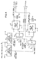
- the pixel error detection circuit 29 is comprised of the circuits shown in FIGS. 4, 5 and 7, which will now be discussed.
- the digital pixel data from ADC 27 is applied to a lamp off comparator 61.
- the comparator 61 compares each digitized pixel in a line scan of pixel data against a reference digital 16 signal. If any digitized pixel is greater in amplitude than 15, the comparator 61 develops a 1 state "lamp off pixel error" signal to indicate an associated defective element in the array 21 during the first mode of operation.
- a lamp off pixel error is applied to an AND gate.
- the AND gate 63 is also applied to the AND gate 63.
- the ⁇ X clock (FIG. 1), the B signal (FIG.3) from inverter 55 (FIG. 2), a diagnostic enable gate or signal (FIG. 5 - to be explained) and the object present signal from senor 39 (FIG.1).
- the AND gate 63 will develop a 1 state LPOERR signal (to indicate a lamp off error) for each lamp off pixel error developed by comparator 61.
- This 1 state LPOERR signal will be developed during the positive alternation of the associated ⁇ X clock, which will occur after the output of the comparator 61 has stabilized.
- Each LPOERR signal is applied to the clock input of lamp off error flip flop 67.
- output A of delay 49 maintains a clear (0 state) signal on the clear input of flip flop 67 until time T 3 and that AND gate 63 cannot generate a LPOERR signal after B goes low at time T 5 . Consequently, AND gate 63 can only develop an LPOERR signal during the 1 second lamp off test period between time T 3 and time T5.
- the first LPOERR signal generated by AND gate 63 during the lamp off test period, T 3 -T 5 clocks the flip flop 67 to cause the flip flop 67 to develop a "lamp off error" signal at its Q output.
- the lamp off error signal from flip flop 67 turns on a LED 69 to indicate that at least one element in array 21 (FIG. 1) is defective during the first mode of operation. This lamp! off error signal can also be applied to the external circuitry 41 for utilization thereby.
- the digital pixel data from ADC 27 is applied to a lamp on comparator 71.
- This comparator 71 compares each digitized pixel in a line scan of pixel data against a reference digital 48 signal. If any digitized pixel is less in amplitude than 48, comparator 71 develops a 1 state "lamp on pixel error" signal to indicate an associated weak element in the array 21 during the second mode of operation.
- the comparator 71 outputs a sequence of lamp on pixel errors, the lamp 15 may be weak, the power supply 35 voltage to lamp 15 may be low, or the whole array 21 of elements may be dirty or defective.
- a lamp on pixel error is applied to an AND gate 73, along with the 0 X clock, the object present signal from sensor 39, the diagnostic enable gate or signal and the C signal (FIG.3) from delay 57(FIG. 2).
- the AND gate 73 will develop a 1 state LPIERR signal (to indicate a lamp on error) for each lamp on pixel error developed by comparator 71.
- This 1 state LPIERR signal will be developed during the positive alternation of the associated 0 X clock, which will occur after the output of the comparator 71 has stabilized.
- Each LPIERR signal is applied to the clock input of lamp on error flip flop 75.
- output C of delay 57 maintains a clear (0 state) signal on the clear input of flip flop 75 until time T7 and that NAD gate 73 cannot generate an L P IERR signal until after C goes high at time T 7 .
- the first LPIERR signal generated by AND gate 73 during the lamp on test period (from time T 7 until another diagnostic operation is initiated at another time T 0 ) clocks the flip flop 75 to cause the flip flop 75 to develop a "lamp on error" signal at its Q output.
- the lamp on error signal from flip flop 75 turns on an LED 77 to indicate that at least one element in array 21 (FIG.1) is defective during the second mode of operation. This lamp on error signal can also be applied to the external circuitry 41 for utilization thereby.
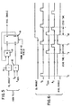
- FIG. 5 a circuit is shown for generating a "diagnostic (diag.) enable” gate or signal which is used by the circuitry of FIG. 7 (to be discussed).
- This diag. enable gate is a synchronous signal which is precisely timed during each scan line during a diagnostic operation.
- the waveforms of FIG. 6 will also be referred to.
- a " ⁇ T inhibit" signal from external circuitry 41 in inverted by a logical inverter 79 and applied to one input of an AND gate 81.
- the output of AND gate 81 is applied to the D input of flip flop 83.
- the Q output of flip flop 83 is connected to the second input of AND gate 81.
- the diag. enable gate is taken from the Q output of the flip flop 83.
- the ⁇ T inhibit signal is in a logical 0 state (until after an evaluation operation is requested by external circuitry 41).
- the inversion of the 0 T inhibit signal by logical inverter 79 causes the AND gate 81 to operate as a repeater of the logical state of the Q output of the flip flop 83.
- the output of delay 43 (see FIGS. 2 and 3) is applied to the clear input of the flip flop 83 to clear that flip flop before time T 1 (FIG. 3).
- the Q and Q outputs of the flip flop 83 are in respective 0 and 1 logical states.
- the output of AND gate 81 thus applies a logic 1 to the D input of flip flop 83.
- the flip flop 83 cannot change its output states until it is clocked.
- Signal P 0 which is developed by pixel counter 25 (FIG. 1) at the start of a scan line (time T E in FIG. 6), is applied through an OR gate 85 to clock the flip flop 83 to change its output states and initiate a diag. enable gate.
- the now 0 state Q output of flip flop 83 is then applied through the enabled AND gate 81 to the D input of flip flop 83.
- pulse P1024 from counter 25 (FIG. 1) is passed through the OR gate 85 to again clock the flip flop 83 to change its output states and terminate the diag. enable gate at time T D for that scan.
- the first operation is the diagnostic operation during which the pixel error tests are performed for each of first (lamp 15 "off") and second (lamp 15 "on") modes of operation.
- the second operation is the evaluation operation during which the results of the pixel error tests are examined.
- the state of the " ⁇ T inhibit" signal will determine whether the system is in a diagnostic operation or an evaluation operation. When 0 T inhibit is low (a logical 0), the system is in a diagnostic operation. Conversely, when 0 T inhibit is high (a logical 1), the system is in an evaluation mode.
- ⁇ T inhibit and diagnostic clear signals from external circuitry 41 are respectively in logical 0 (low) and logical 1 (high) states and there are no diagnostic read clocks applied from external circuitry 41.
- a diagnostic operation begins with the initial turn on of the system or can be begun at any time after the system is in operation by utilizing an external reset pulse from external circuitry 41 to momentarily close electronic switch 59 to short out capacitor C1 in the on/off control circuit 31 of FIG. 2. It will also be recalled that a 1 state diagnostic enable gate (FIGS. 5 and 6) is generated during each scan line during the 1-second long diagnostic operation.
- the diagnostic enable gate causes a multiplexer (MUX) 87 0 to pass any LPOERR (lamp off error) signals to the count input (C) of a lamp off error counter 89 0 to be counted.
- MUX multiplexer
- Each LPOERR signal increments the counter 89 0 by a count of 1.
- the output count of counter 89 0 is also applied to a latch 91 0 , which is enabled by each 1 state output of an AND gate 93 0 to latch the output count of the counter 89 0 .
- the B signal (FIG. 2) and the P1024 pulse (FIG. 1) are inputted to the AND gate 93 0 .
- the B signal is in a logical 1 state to enable the AND gate 93 0 at each P1024 pulse time to latch the output count of counter 89 0 into latch 91 0 .
- This output count of counter 89 0 is the total number of failed off pixels that were developed in the prior scan during the lamp off test. This total number of failed off pixels, that is stored in the latch 91 0 , is applied to the external circuitry 41.
- Each output count of counter 89 0 is also applied as a 10-bit address to a lamp off error RAM (random access memory) 95.
- RAM 95 0 is a 1K x 10-bit RAM which can store 1024 different 10-bit words.
- a 10-bit address from counter 89 0 and a RAM storage capacity of 1024 words are needed in case all of the 1024 pixels in the array 21 (FIG. 1) are defective.
- the pixel number or address AO-A9 from pixel counter 25 (FIG. 1) is applied to a 10-bit tri-state buffer 97 0 , which buffer can be implemented by means of two Fairchild 74LS367A 3-state buffers.
- Buffer 97 0 is enabled by a diagnostic enable signal (from the Q output of flip flop 83 in FIG. 5) to pass the pixel address AO-A9 to RAM 95 0 via data lines (DATA).
- the ⁇ X pixel clocks, the diagnostic enable signal and any LPOERR pixel error signals are inputted to a NAND gate 99 0 to enable the NAND gate 99 0 to develop a W 0 /R 0 signal to control the write/read operations of the RAM 95 0 .
- Any LPOERR error that occurs during the period of the diagnostic enable gate is passed at clock time ⁇ X through the NAND gate 99 0 as a logical 0 write signal ( W O ) to enable the RAM 95 0 to write the address (AO-A9) of the failed off pixel into the location of the RAM 95 0 specified by the address count from the counter 89 0 .
- RAM 95 0 sequentially stores the address of each failed pixel number that occured during a first mode scan (lamp 15 "off").
- NAND gate 99 0 When at least one of the inputs to NAND gate 99 0 is in a 0 state (i.e. no pixel error developed during a given pixel time), NAND gate 99 0 develops a logical 1 read signal (R 0 ).
- the lamp off error counter 89 0 is cleared and a new count of LPOERR errors is developed by the counter 89 0 .
- the counter 89 0 will again be incremented by the LPOERR to again cause the address of any failed pixel number that occurs during that first mode scan to be rewritten into the location of RAM 95 0 that corresponds with the associated count of counter 89 0 .
- Such clearing of the counter 89 0 at the end of each scan is necessary to prevent the counter 89 0 from accumulating the same pixel errors in consecutive scan lines during the diagnostic operation.
- Counter 89 0 is cleared at the end of each scan line in the following manner.
- the diagnostic clear and 0 T inhibit signals are applied to a NAND gate 101, which has its output coupled to a first input of another NAND gate 103. It will be recalled that the diagnostic clear signal is high and the 0 T inhibit signal is low during the diagnostic operation. Therefore, the NAND gate 101 will develop and apply a logical 1 state signal to the first input of NAND 103 during the entire diagnostic operation.
- Clock 0 ⁇ T is applied to a second input of the NAND gate 103 which has its output, in turn, connected to the clear input of counter 89 0 .
- the clock 0 ⁇ T which occurs at the end of each scan line, will clear the count of the counter 89 0 at the end of each scan line that occurs during the diagnostic operation.
- the system starts the lamp on test.
- the system uses curcuits 87 1 , 89 1 , 91 1 , 95 1 , 97 1 and 99 1 , which are respectively similar in structure and operation to the circuits 87 0 , 89 Q , 91 0 , 95 0 , 97 0 , and 99 0 .
- the circuits 87 1 , 89 1 , 9 11 , 95 1 , 971 and 99 1 utilize the LPIERR (lamp on error) signal applied to MUX 87 1 to develop the total "number of failed on pixels" during a scan at the output of lamp on error counter 89 1 and to sequentially store in lamp on error RAM 95 1 the address of each failed pixel number that occured during a second mode scan (lamp 15 "on").
- the W 1 /R 1 signal from NAND gate 99 1 is also applied to the RAM 95 1 to control the write/read operation of the RAM 95 1 in the same manner discussed before, but as a function of any LPIERR errors developed during the second mode of operation.
- the rising edge of the 1-state diagnostic enable signal (from the Q output of flip flop 83 in FIG. 5) clocks the current output count of counter 89 1 ) into latch 91 1 .
- This current output is the total number of failed on pixels that were developed in the prior scan of the lamp on test.
- the current total number of failed on pixels, that is now stored in latch 91 1 is also applied to the external circuitry 41.
- the following 0 ⁇ T clock clears the count of counter 89 1 .
- the evaluation operation allows the system to read out the addresses of the failed pixels from the RAMs 95 0 and 95 1 .
- the 0 ⁇ T inhibit signal asynchronously changes, or is asynchronously changed, to a high level or logical 1.
- the inversion of this 1 state 0 ⁇ T inhibit signal by inverter 79 disables AND gate 81 and thereby prevents the flip flop 83 from generating any further diagnostic enable gates during the evaluation operation.
- the current diagnostic enable gate being generated by the flip flop 83 is allowed to be completed before the diagnostic operation is ended.
- latches 91 0 and 91 1 respectively contain the final numbers of failed off and failed on pixels that were produced during the diagnostic operation.
- external circuitry 41 has control of the pixel error detection circuit 29 to find out what specific pixel errors were detected during the diagnostic operation.
- the 1 state 0 ⁇ T inhibit signal and the unchanged 1 state diagnostic clear signal cause the NAND gate 101 to output a logical 0 to NAND gate 103.
- the output of the NAND gate 103 applies a 1 state to the clear inputs of counters 89 0 and 89 1 .
- the 1 state signal from NAND 101 prevents the NAND gate 103 from clearing the counts of the counters 89 0 and 89 1 at the time of the end of the scan clock 0 T .
- the MUX's 87 0 and 87 1 are still enabled by the current 1 state diagnostic enable gate. It should be recalled that the current total number of failed off pixels has been stored in latch 91 0 at the end of the previous lamp off test. In addition, during the current lamp on test, no LPOERR error signals are developed and hence none are applied to MUX 87 0 . However, the LPIERR error signals that are detected during the current second mode scan (lamp 15 "on”) are sequentially passed to the lamp on error counter 89 1 to be counted and subsequently stored in the latch 91 1 as the total number of failed on pixels, as previously discussed.
- the current diagnostic enable gate or signal continues at a 1-state level until it is completed at the time T DE of the P 1024 signal, as shown in FIG. 6.
- the diagnostic enable signal changes to a 0 state.
- the 0-state of the diagnostic enable signal causes the MUXs 87 0 and 87 1 to select the diagnostic read clock position.
- no diagnostic read clocks are generated by the external circuitry 41 at this time. Hence, no signals are passed by the MUXs at this time.
- the 0-state of the diagnostic enable signal also cuases NAND gate 99 0 to apply a 1 state read signal (R O ) to RAM 95 0 and NAND gate 99 1 to apply a 1 state read signal (R 1 ) to RAM 95 1 .
- both of the RAMs 95 0 and 95 1 are in their read modes.
- the 10-bit outputs of the RAMs 95 0 and 95 1 are respectively applied to latches 105 0 and 105 1 .
- these latches 105 0 and 105 1 cannot pass data from the RAMs 95 0 and 95 1 to the external circuitry 41 until the latches start receiving diagnostic read clocks from the external circuitry 41.
- each of the latches 91 0 , 91 1 , 105 0 and 105 1 is a 10-bit latch which can be. implemented by means of three Fairchild 74LS375 4-bit latches. It should also be noted that, after being cleared, each of the counters 89 0 and 89 1 develops a 0 count address output.
- the lamp off error just indicates that at least one of the 1024 pixels (in the array 21) is defective when the lamp 15 is "off".
- the lamp on error just indicates that at least one of the 1024 pixels is defective when the lamp 15 is "on”. Neither of these signals provides any information as to the total number or identity of failed or defective pixels. The other four signals supply this missing information for the lamp off and lamp on tests.
- the next 0 ⁇ T clock that is applied to NAND gate 103 causes NAND gate 103 to develop a 0 state signal to clear the count from both of the counters 89 0 and 89 1 .
- the 0 address counts from the counters 89 0 and 89 1 cause the RAMs 95 0 and 95 1 to respectively apply the failed pixel numbers stored in their 0 address locations to the inputs of the latches 105 0 and 105 1 , respectively.
- the system is now ready to start outputting data to the external circuitry 41 to identify all of the defective pixels that were detected during both of the lamp off and lamp on tests during the diagnostic operation.
- Diagnostic read clocks are now supplied from the external circuitry 41 to accomplish the outputting of data from the RAMs 95 0 and 95 1 .
- These diagnostic read clocks may be derived from switches, push buttons, a diagnostic processor, discrete logic circuitry or from any other suitable source.
- the first diagnostic read clock enables latch 105 0 to store the lamp off failed pixel number or address being outputted from location 0 of RAM 95 0 and enables latch 105 1 to store the lamp off failed pixel number or address being outputted from location 0 of RAM 95 1 .
- This first diagnostic read clock also increments the counters 89 0 and 89 1 to output address counts of 1.
- the failed pixel numbers stored in location 1 of the RAMs 95 0 and 95 1 are respectively read out of the RAMs and applied to the inputs of latches 105 0 and 105 1 .
- this new data from the RAMs 95 0 and 95 1 will not be latched into the latches 105 0 and 105 1 until the second diagnostic read clock occurs.
- the previous pixel number data being outputted from the RAMs 95 0 and 95 1 is latched into latches 105 0 and 105 1 , while the counters 89 0 and 89 1 are again incremented by one to cause the RAMs to output new data to the inputs of latches 105 0 and 105 1 .
- External circuitry 41 could also include LED (light emitting diode) circuits (not shown) to visually indicate the defective pixel numbers.
- the pixel failure information stored in the latches 91 0 and 91 1 and/or RAMs 95 0 and 95 1 could be used to determine the seriousness of the problem with an imaging sensor array 21 such as a CCD. If no pixel failures are detected the system may be operating perfectly. If, for example, less than 5 pixel failures are detected, the degradation in the imaging of objects or documents may be so minor that only an equipment warning status would be warranted. In this case the system would still be operated while a technician was summoned to repair the imaging sensor array 21 at his convenience. On the other hand, if, for example, 5 or more pixel failures are detected, the degradation in the imaging of objects or documents may be so severe that an equipment failure status may be required. In this case the equipment should be turned off and a technician summoned immediately to correct the problem.
- the invention thus provides a system and method for automatically testing, detecting and identifying any picture element failures in a multielement imaging sensor array during each of lamp off and lamp on modes of operation.
Abstract
Description
- This invention relates to electro-optical imaging systems of the kind including: a reference background adapted to reflect radiant energy impinging thereon; illuminating means adapted to illuminate said reference background during an on mode of operation; scanning means including at least one array having N photosensitive elements adapted to provide N reference pixed signals for each scan of said reference background; and error signal generating means including comparison means adapted to produce an error signal whenever any reference pixel signal is less than a predetermined reference level.
- An electro-optical imaging system of the kind specified is known from U.S. Patent Specification No. 4,287,536. The known electro-optical imaging system includes a pair of multi-element scanning arrays arranged to scan a calibration strip and thereby provide outputs which are each compared with a preset reference level to develop a corrective signal which controls the gain of each of the arrays. The known system also discloses an arrangement wherein the calibration strip is scanned in each of a plurality of modes and the image data output is applied to a microprocessor unit which compares the image signal output with a predetermined minimum voltage level or threshold. According as the comparison output represents the image signal as being above or below the minimum threshold a binary "1" or a binary "0" is loaded into an associated location in a random access memory (RAM). During a subsequent scanning operation of an object to be scanned, the contents of the RAM are utilized such that a stored "0", indicating a "bad" photosensitive element, causes the previous pixel signal to be substituted for the "bad" pixel signal. It will be appreciated that the failure of a photosensitive element may be indicative of an impending partial or total failure of the photosensitive array. A problem experienced with the known system that unacceptable system outputs may be produced resulting from such photosensitive array failure.
- It is an object of the present invention to provide an electro-optical imaging system of the kind specified wherein the likelihood of unacceptable outputs being produced is reduced.
- Therefore, according to the present invention where is provided an electro-optical imaging system of the kind specified characterized by indicator means adapted to indicate to an operator that at least one of said photosensitive elements in said array is defective.
- It will be appreciated that a system according to the invention has the advantage that an operator is made aware that one or more photosensitive elements in the array is defective. This gives the operator an early warning indication of a possible impending failure of the array. With such an indication, the operator would have an opportunity to arrange for the array to be serviced by repair or replacement in time before any partial or total failure of the array actually occurs.
- One embodiment of the invention will now be described by way of example, with reference to the accompanying drawings, in which:
- FIG. 1 is a schematic block diagram of an electro-optical imaging apparatus incorporating the invention;
- FIG. 2 is a composite schematic block and circuit diagram of the on/off control circuit of FIG. 1;
- FIG. 3 illustrates waveforms useful in explaining the operation of the on/off control circuit of FIG. 1:
- FIGS. 4, 5, 7A and 7B are schematic block diagrams which in combination, form the pixel error detection circuit of FIG. 1; and
- FIG. 6 illustrates waveforms useful in explaining the operation of the circuit shown in FIG. 5.
- Referring now to the drawings, FIG. 1 discloses a schematic block diagram of a preferred embodiment of the invention. The invention is shown in a video camera environment or application for scanning information from objects or documents.
- In the normal imaging of an object, the following operation occurs. A reference background 11, which is preferably white in color, is mounted near or adjacentto a moving track or moving conveyor line or mounted on a rotating
drum 13. When no object is present, the reference background is illuminated by radiant energy, such as by light from a suitable light source orlamp 15. - An object or
document 17 to be imaged can be either stationary or transported by the moving track, moving conveyor line or rotatingdrum 13 along a path between the reference background 11 and alens assembly 19. As theobject 17 is moved across the reference background, it is illuminated by thelight source 15. A reflected optical image of theobject 17 is focused by thelens assembly 19 onto the face of animaging sensor array 21. Theimaging sensor array 21 could comprise any suitable array such as, for example, an array of photodiodes, a photoarray or a charge coupled device (CCD) array. - For purposes of this description, the
array 21 is 1024-element CCD array such as, for example, a Model 133/143 CCD, manufactured by CCD Imaging Products Division, Fairchild Camera & Instrument Corporation. - Transport clocks ØX and transfer clocks 0 T from a timing and
control circuit 23 enable theimaging sensor array 21 to generate a plurality of scan lines of anobject 17 as the object traverses the scan position of thearray 21. Each scan line of thearray 21 develops 1024 picture elements or pixels, with each pixel having a particular one of 64 gray scale values, which value represents a portion of theobject 17 being scanned. The composite of these scan lines of the object provides a signal image of theobject 17 being scanned. - Transport clocks ØX control the readout rate of video data from the 1024 cells in the
imaging sensor array 21 at a rate of approximately 270 nanoseconds per pixel. A transfer clock ØT occurs at the end of each line scan and controls the integration time of thearray 21. This so-called integration time of thearray 21 is analogous to the exposure time in conventional cameras. The scan interval or interpulse period of the transfer clock ØT is approximately 285 microseconds. - Each transport clock ØX increments an 11-bit, synchronous,
binary pixel counter 25 by one, causing its output to sequentially develop address counts or addresses from 0 to 1063. The pixel clocks ØX which occur between- theaddresses 0 through 1023 are used to sequentially clock out video pixel signals from the 1024 cells orelements 0 through 1023 of thearray 21. Thepixel clocks 0x which occur between addresses 1024 through 1062 may be utilized to clock out black and white references inside thearray 21 for purposes beyond the scope of this invention. - For purposes of synchronization the 0T clock, which occurs at the end of a scan and during the pixel count of 1063, is used to synchronously reset the
counter 25 to an address count of 0 at the following 0X clock time in order to start a new line scan of thearray 21. -
Counts 0 and 1024 ofcounter 25 are internally decoded by thecounter 25 to develop signals P0 and P 1024 which respectively represent the first and 1024th transport clocks in each line scan. Although thecounter 25 develops an 11-bit output, only the 10 least significant bits AO-A9 are outputted for further utilization by the system. - The logical inverse of each transport clock 0y, or
Ø X, is applied from timing andcontrol circuit 23 to enable an analog-to-digital converter (ADC)circuit 27 to digitize the video pixel signals from thearray 21 to produce a corresponding scan of digitized pixels or pixel data for each scan line of thearray 21. It should be noted that where animaging sensor array 21 has two output lines or channels, such as are contained in a Fairchild Model 133/143 CCD, theADC circuit 27 may contain two separate ADCs for respectively digitizing the two channel outputs and, in addition, circuitry for interlacing the two digitized channel outputs into one composite output. CCD interlacing techniques, which form no part of this invention, are described in detail in U.S. Patent No. 3,911,467. - Each of the digitized pixels from the
ADC circuit 27 has a gray scale value which is six bits wide; Each digitized pixel can have one of the 64 gray scale values ranging from completely black (a digital value of 000000) to completely white (a digital value of111111). - The scans of pixel data from the
ADC circuit 27 may be applied to othervideo processing circuits 28 where, for example, the digitized image of a scannedobject 17 can be conventionally reconstructed along X and Y coordinates, scan line by scan line. However, further utilization of the pixel data by othervideo processing circuits 28 is beyond the purview of this invention and, hence, will not be further discussed. - The invention automatically and repeatedly tests each scan of pixel data from
ADC 27 for any defective elements or cells in theimaging sensor array 21 during a "diagnostic operation". In the performance of such tests on the pixel data, the pixel data fromADC 27, the ØX and 9T clocks from timing andcontrol 27, and the PO and P1024 signals and AO-A9 addresses frompixel counter 25 are applied to a pixelerror detection circuit 29. - Because of the different reflectivities of different objects being imaged by the
array 21, no pixel data testing can be accurately and repeatably performed by the system of FIG. 1 when anobject 17 is being imaged. Consequently, whenever anobject 17 is detected in thetrack 13, a 0 state object (obj.) present signal prevents thedetection circuit 29 from testing the pixel data. - To control the timing of the diagnostic operation of the system, an on/off
control circuit 31 is included to initiate an initial diagnostic operation of the system after power is initially applied to the system and to initiate a subsequent diagnostic operation each time it receives an external (ext.) reset signal. - Each time that the
control circuit 31 initiates a diagnostic operation, it sends control signals to thedetection circuit 29 to enable thecircuit 29 to sequence through different tests on the pixel data fromADC 27. As long as noobject 17 is detected in thetrack 13, thedetection circuit 29 will be enabled by a 1 state obj. present signal to complete a diagnostic operation. - Each time that the
control circuit 31 initiates a diagnostic operation, it also supplies a lamp control signal to control the operation of aprimary power relay 33 to either supply or not supply primary power (not shown) to apower supply 35 as a function of the amplitude of the lamp control signal. - During a first mode of operation, the lamp control signal has an insufficient amplitude to energize the
relay 33. As a result, thepower supply 35 provides no power to thelamp 15 and thelamp 15 is "off". With thelamp 15 "off", theimaging sensor array 21 scans the unilluminated reference background 11 (provided that noobject 17 is present in thetrack 13 during this first mode of operation). During this first mode of operation, the control signals fromcontrol circuit 31 enable thedetection circuit 29 to test the pixel data with thelamp 15 "off". - After a suitable time delay, the
control circuit 31 changes the amplitude of the lamp control signal to end the first mode of operation and start the second mode of operation. During the second mode of operation, the control signal has a sufficient amplitude to energize therelay 33. Thepower supply 35 therefore supplies power to turn "on" thelamp 15. With thelamp 15 "on", theimaging sensor array 21 scans the illuminated reference background 11 (provided that noobject 17 is present in thetrack 13 during this second mode of operation). During this second mode of operation, the control signals fromcontrol circuit 31 enable thedetection circuit 29 to test the pixel data with thelamp 15 "on". - Once the system has entered the second mode of operation, it remains in this second mode of operation to enable the
detection circuit 29 to repeatedly test the pixel data with thelamp 15 "on". However, even this second mode of operation is temporarily interrupted each time that anobject 17 to be imaged by thearray 21 is detected in thetrack 13. More specifically, as anobject 17 moves down thetrack 13 toward the reference background 11, it passes between a light emitting diode (LED) 37 andlight sensor 39 which are respectively positioned on opposite sides of thetrack 13. The passage of anobject 17 between theelements LED 37 andsensor 39, causing thesensor 39 to develop a 0 state object (obj.) present signal to temporarily interrupt the operation of thedetection circuit 29. - After a suitable time delay after the trailing edge of the
object 17 has cleared the path between theLED 37 andsensor 39, the object present signal returns to a 1 state to enable thedetection circuit 29 to again test each line scan of pixel data derived from the reference background 11. Such a suitable delay can be readily determined from the known speed of thetrack 13 after theobject 17 clears the path between theLED 37 andsensor 39. This known time delay (not shown) can be readily added to thesensor 39 output. - The pixel failure information that was derived during a diagnostic operation can be examined by
external circuitry 41 during an evaluation operation.External circuitry 41 can be any suitable circuit, such as switches, push buttons, a microprocessor or discrete logic, for selectively generating an external reset pulse, a 0T inhibit signal, a diagnostic clear (diag. clr.) signal and diagnostic read clocks (diag. read clk) to read out any pixel failure information from thedetection circuit 29. - Referring now to FIGS. 2 and 3, FIG. 2 illustrates a composite schematic block and circuit diagram of the on/off
control circuit 31 of FIG. 1, while FIG. 3 illustrates waveforms useful in explaining the operation of thecontrol circuit 31. - Initially, the system of FIG. 1 is turned off and no power is applied anywhere. At time TO (FIG.3), when power is initially applied to the system, power supplies (not shown) are brought up to their operating potentials. A positive five volts (+5V) from one of the power supplies is applied to a terminal 42 in a one-half second logic
stable delay circuit 43. A resistor R1 and capacitor C1 are serially connected to each other between the terminal 42 and ground. The voltage across Cl, EC1' which is applied to the input of a Schmitt buffer (S.B.) 45, is low at the time the +5V is applied to the terminal 42. As a result, the output ofbuffer 45 is also low. This low output ofbuffer 45 is applied to the clear input of a lampcontrol flip flop 47, which causes theflip flop 47 to develop at its Q output a low level lamp control signal. The low level lamp control signal fromflip flop 47 turns off therelay 31 which, as indicated in FIG. 1, turns off thepower supply 35 and, hence, turns offlamp 15. - The purpose of the logic
stable delay 43 is to provide a delay of approximately one half of a second for the stabilization of the logic power supplies in the system. At time T1(FIG.3) after a delay of approximately one half of a second, the charge EC1 on the capacitor C1 has increased to a voltage sufficient to trigger theSchmitt buffer 45 to change its output state from low to high. Thus, the high output ofdelay 43 removes the clear signal (0 state) from the lampcontrol flip flop 47. However, until theflip flop 47 is subsequently clocked, it continues to develop a low level lamp control signal. - The high output of
delay 43 is also applied to a lamp offstable delay 49 to provide an additional 1 second delay for thelamp 15 to stabilize in its off state. - Within the delay 49 a resistor R2 and capacitor C2 are serially connected to each other between the output of
buffer 45 and ground. A diode CR1 is connected in parallel to the resistor R2. The junction of R2 and C2 is connected to the input of aSchmitt buffer 51. In response to the output ofbuffer 45 changing to a high level, capacitor C2 starts charging up toward that high level. At time T3 (FIG. 3), after a delay of about 1 second, the charge EC2 on the capacitor C2 triggers theSchmitt buffer 51 to change its output state from low to high. This output ofbuffer 51 is the output A ofdelay 49, as shown in FIG. 3. - In a similar manner, at time T3 the high level output A of
delay 49 is also applied to a 1 second lamp off-to-onstable delay 53, which is similar in structure and operation to thedelay 49. At time T5, after another 1 second delay, the output B ofdelay 53 changes from low to high to clock the lampcontrol flip flop 47 on its rising edge. Upon being clocked, the lampcontrol flip flop 47 develops at its Q output a high level lamp control signal which energizes therelay 31, causingpower supply 35 to be turned on and to turn onlamp 15. - The B signal from the output of
delay 53 is inverted by alogical inverter 55 to develop a B signal. - As shown in FIG. 3, the lamp off pixel error test was conducted for a period of .1 second between times T3 and T5. During this 1 second period of time, approximately 3500 separate scan lines of pixel data could have been tested for pixel errors after the
lamp 15 was turned off and stabilized (provided that noobject 17 was detected in thetrack 13 during this time). - The purpose of the lamp off-to-on
stable delay 53 is to provide a delay of approximately 1 second for thelamp 15 to stabilize in its on state before any lamp on pixel error tests are conducted by detection circuit 29 (FIG.1). - At time T5 the high level output B of
delay 53 is also applied to a 1 second lamp onstable delay 57, which is similar in structure and operation to thedelay 49. At time T71 after a final 1 second delay, the output C ofdelay 57 changes from low to high. From time T7 on, the lamp on pixel error test can be conducted on separate scan lines of pixel data after thelamp 15 has been turned on and stabilized (whenever noobject 17 is detected in the track 13). - A
suitable switch 59, such as an electronic switch, is coupled across capacitor C1. Innormal operation switch 59 is open. However, switch 59 is controlled by an external reset signal from external circuitry 41 (FIG.1) to momentarily close and discharge capacitor C1 to initiate a diagnostic operation whenever desired or required. - It should be noted that the on/off
control circuit 31 could have been implemented in a manner different than that shown in FIG. 2 by using, for example, a field programmable logic array (FPLA), a counter and suitable data storage units to obtain the sequence of delays and control signals shown in FIGS. 2 and 3. The FPLA would be programmed to respond to Boolean equations to generate the sequence of delays and control signals for both thelamp 15 "on" andlamp 15 "off" pixel data testing. Furthermore, an analog delay circuit, other than the type illustrated in FIG. 2, also could have been utilized. - The pixel
error detection circuit 29 is comprised of the circuits shown in FIGS. 4, 5 and 7, which will now be discussed. - Referring now to FIG. 4, during the first mode of operation (when
lamp 15 is "off") the digital pixel data fromADC 27 is applied to a lamp offcomparator 61. Thecomparator 61 compares each digitized pixel in a line scan of pixel data against a reference digital 16 signal. If any digitized pixel is greater in amplitude than 15, thecomparator 61 develops a 1 state "lamp off pixel error" signal to indicate an associated defective element in thearray 21 during the first mode of operation. - A lamp off pixel error is applied to an AND gate. Also applied to the AND
gate 63 is theØ X clock (FIG. 1), the B signal (FIG.3) from inverter 55 (FIG. 2), a diagnostic enable gate or signal (FIG. 5 - to be explained) and the object present signal from senor 39 (FIG.1). As long as noobject 17 is present in the track 13 (FIG.1) and a 1 state lamp off pixel error occurs during a 1 state diagnostic enable gate before the end of the lamp off test period (T3-TS in FIG. 3), the ANDgate 63 will develop a 1 state LPOERR signal (to indicate a lamp off error) for each lamp off pixel error developed bycomparator 61. This 1 state LPOERR signal will be developed during the positive alternation of the associatedØ X clock, which will occur after the output of thecomparator 61 has stabilized. Each LPOERR signal is applied to the clock input of lamp offerror flip flop 67. - Referring also to FIG. 3, it can be seen that output A of
delay 49 maintains a clear (0 state) signal on the clear input offlip flop 67 until time T3 and that ANDgate 63 cannot generate a LPOERR signal after B goes low at time T5. Consequently, ANDgate 63 can only develop an LPOERR signal during the 1 second lamp off test period between time T3 and time T5. - The first LPOERR signal generated by AND
gate 63 during the lamp off test period, T3-T5, clocks theflip flop 67 to cause theflip flop 67 to develop a "lamp off error" signal at its Q output. The lamp off error signal fromflip flop 67 turns on aLED 69 to indicate that at least one element in array 21 (FIG. 1) is defective during the first mode of operation. This lamp! off error signal can also be applied to theexternal circuitry 41 for utilization thereby. - During the second mode of peration (when
lamp 15 is "on") the digital pixel data fromADC 27 is applied to a lamp oncomparator 71. Thiscomparator 71 compares each digitized pixel in a line scan of pixel data against a reference digital 48 signal. If any digitized pixel is less in amplitude than 48,comparator 71 develops a 1 state "lamp on pixel error" signal to indicate an associated weak element in thearray 21 during the second mode of operation. However, it should be realized that, if thecomparator 71 outputs a sequence of lamp on pixel errors, thelamp 15 may be weak, thepower supply 35 voltage tolamp 15 may be low, or thewhole array 21 of elements may be dirty or defective. - A lamp on pixel error is applied to an AND
gate 73, along with the 0X clock, the object present signal fromsensor 39, the diagnostic enable gate or signal and the C signal (FIG.3) from delay 57(FIG. 2). As long as noobject 17 is present in the track 13 (FIG. 1) and a 1 state lamp on pixel error occurs during a 1 state diagnostic enable gate after the start of the lamp on test period (T7 in FIG. 3), the ANDgate 73 will develop a 1 state LPIERR signal (to indicate a lamp on error) for each lamp on pixel error developed bycomparator 71. This 1 state LPIERR signal will be developed during the positive alternation of the associated 0X clock, which will occur after the output of thecomparator 71 has stabilized. Each LPIERR signal is applied to the clock input of lamp onerror flip flop 75. - Referring again also to FIG. 3, it can be seen that output C of
delay 57 maintains a clear (0 state) signal on the clear input offlip flop 75 until time T7 and thatNAD gate 73 cannot generate an LPIERR signal until after C goes high at time T7. - The first LPIERR signal generated by AND
gate 73 during the lamp on test period (from time T7 until another diagnostic operation is initiated at another time T0) clocks theflip flop 75 to cause theflip flop 75 to develop a "lamp on error" signal at its Q output. The lamp on error signal fromflip flop 75 turns on anLED 77 to indicate that at least one element in array 21 (FIG.1) is defective during the second mode of operation. This lamp on error signal can also be applied to theexternal circuitry 41 for utilization thereby. - It can be seen in FIG. 4 that the pixel data from
ADC 27 is simultaneously applied to the inputs of both ofcomparators comparator 71 during the first mode of operation (lamp 15 "off"), ANDgate 73 will not develop any LPIERR signals during this period of time (T3-T5) since the C signal (FIG. 3) is in a 0 state to disable ANDgate 73. In a similar manner a "lamp off pixel error" can readily be generated bycomparator 61 during the second mode of operation (lamp 15 "on"). However, a 0 state B signal will prevent the ANDgate 63 from generating any LPOERR signals during this period of time (from T5 on)_ - Referring now to FIG. 5, a circuit is shown for generating a "diagnostic (diag.) enable" gate or signal which is used by the circuitry of FIG. 7 (to be discussed). This diag. enable gate is a synchronous signal which is precisely timed during each scan line during a diagnostic operation. For ease of understanding the operation of the circuit of FIG. 5, the waveforms of FIG. 6 will also be referred to.
- A "ØT inhibit" signal from external circuitry 41 (FIG. 1) in inverted by a
logical inverter 79 and applied to one input of an ANDgate 81. The output of ANDgate 81 is applied to the D input offlip flop 83. TheQ output offlip flop 83 is connected to the second input of ANDgate 81. The diag. enable gate is taken from the Q output of theflip flop 83. - As shown in FIG. 6 the ØT inhibit signal is in a logical 0 state (until after an evaluation operation is requested by external circuitry 41). Thus, the inversion of the 0T inhibit signal by
logical inverter 79 causes the ANDgate 81 to operate as a repeater of the logical state of theQ output of theflip flop 83. - The output of delay 43 (see FIGS. 2 and 3) is applied to the clear input of the
flip flop 83 to clear that flip flop before time T1 (FIG. 3). Upon being cleared, the Q and Q outputs of theflip flop 83 are in respective 0 and 1 logical states. The output of ANDgate 81 thus applies alogic 1 to the D input offlip flop 83. However, theflip flop 83 cannot change its output states until it is clocked. - Signal P0, which is developed by pixel counter 25 (FIG. 1) at the start of a scan line (time TE in FIG. 6), is applied through an
OR gate 85 to clock theflip flop 83 to change its output states and initiate a diag. enable gate. The now 0 state Q output offlip flop 83 is then applied through the enabled ANDgate 81 to the D input offlip flop 83. - After 1024 digitized pixels (0-1023) in the pixel data from
ADC 27 have been processed by the circuitry of FIG. 4, pulse P1024 from counter 25 (FIG. 1) is passed through theOR gate 85 to again clock theflip flop 83 to change its output states and terminate the diag. enable gate at time TD for that scan. - It can therefore be seen that, during each line scan that occurs during the diagnostic operation, the PO and P1024 pulses respectively initiate and terminate the diag. enable gate associated with that line scan. As a result, a diagnostic test for defective pixels is performed during each scan line that occurs during the diagnostic operation.
- As shown in FIG. 6, there may be a "dead time" between the end of a diagnostic enable gate (at time TD) in one line scan and the start of the next line scan (at time TE). During that dead time, no pixel data from ADC 27 (FIG. 1) is being processed by the pixel
error detection circuit 29. As mentioned before, this is a period of time in a line scan in which black and white references internal to theimaging sensor array 21 may be clocked out of the array. - Referring now to FIGS. 7A and 7B, the last part of the circuitry of the pixel
error detection circuit 29 will now be discussed. - As mentioned before there are basically two operations of the system of FIG. 2. The first operation is the diagnostic operation during which the pixel error tests are performed for each of first (
lamp 15 "off") and second (lamp 15 "on") modes of operation. The second operation is the evaluation operation during which the results of the pixel error tests are examined. Essentially the state of the "ØT inhibit" signal will determine whether the system is in a diagnostic operation or an evaluation operation. When 0T inhibit is low (a logical 0), the system is in a diagnostic operation. Conversely, when 0T inhibit is high (a logical 1), the system is in an evaluation mode. - During a diagnostic operation the ØT inhibit and diagnostic clear signals from
external circuitry 41 are respectively in logical 0 (low) and logical 1 (high) states and there are no diagnostic read clocks applied fromexternal circuitry 41. As explained in the discussion on FIGS. 2 and 3, a diagnostic operation begins with the initial turn on of the system or can be begun at any time after the system is in operation by utilizing an external reset pulse fromexternal circuitry 41 to momentarily closeelectronic switch 59 to short out capacitor C1 in the on/offcontrol circuit 31 of FIG. 2. It will also be recalled that a 1 state diagnostic enable gate (FIGS. 5 and 6) is generated during each scan line during the 1-second long diagnostic operation. - The diagnostic enable gate causes a multiplexer (MUX) 870 to pass any LPOERR (lamp off error) signals to the count input (C) of a lamp off error counter 890 to be counted. Each LPOERR signal increments the
counter 890 by a count of 1. Thus, thecounter 890 keeps track of the total number of pixel errors that occur during a scan. The output count ofcounter 890 is also applied to a latch 910, which is enabled by each 1 state output of an AND gate 930 to latch the output count of thecounter 890. TheB signal (FIG. 2) and the P1024 pulse (FIG. 1) are inputted to the AND gate 930. - During each scan in the first mode of operation (
lamp 15 "off"), theB signal is in a logical 1 state to enable the AND gate 930 at each P1024 pulse time to latch the output count ofcounter 890 into latch 910. This output count ofcounter 890, at the time of the P1024 pulse, is the total number of failed off pixels that were developed in the prior scan during the lamp off test. This total number of failed off pixels, that is stored in the latch 910, is applied to theexternal circuitry 41. - Each output count of
counter 890 is also applied as a 10-bit address to a lamp off error RAM (random access memory) 95. RAM 950 is a 1K x 10-bit RAM which can store 1024 different 10-bit words. A 10-bit address from counter 890 and a RAM storage capacity of 1024 words are needed in case all of the 1024 pixels in the array 21 (FIG. 1) are defective. - The pixel number or address AO-A9 from pixel counter 25 (FIG. 1) is applied to a 10-bit tri-state buffer 970, which buffer can be implemented by means of two Fairchild 74LS367A 3-state buffers. Buffer 970 is enabled by a diagnostic enable signal (from the
Q output offlip flop 83 in FIG. 5) to pass the pixel address AO-A9 to RAM 950 via data lines (DATA). - In the first modeof operation (
lamp 15 "off"), the ØX pixel clocks, the diagnostic enable signal and any LPOERR pixel error signals are inputted to a NAND gate 990 to enable the NAND gate 990 to develop aW 0/R0 signal to control the write/read operations of the RAM 950. Any LPOERR error that occurs during the period of the diagnostic enable gate is passed at clock time ØX through the NAND gate 990 as a logical 0 write signal (W O) to enable the RAM 950 to write the address (AO-A9) of the failed off pixel into the location of the RAM 950 specified by the address count from thecounter 890. In this manner RAM 950 sequentially stores the address of each failed pixel number that occured during a first mode scan (lamp 15 "off"). When at least one of the inputs to NAND gate 990 is in a 0 state (i.e. no pixel error developed during a given pixel time), NAND gate 990 develops a logical 1 read signal (R0). - At the end of each scan line during the diagnostic operation, the lamp off
error counter 890 is cleared and a new count of LPOERR errors is developed by thecounter 890. During the next scan thecounter 890 will again be incremented by the LPOERR to again cause the address of any failed pixel number that occurs during that first mode scan to be rewritten into the location of RAM 950 that corresponds with the associated count ofcounter 890. Such clearing of thecounter 890 at the end of each scan is necessary to prevent thecounter 890 from accumulating the same pixel errors in consecutive scan lines during the diagnostic operation. -
Counter 890 is cleared at the end of each scan line in the following manner. The diagnostic clear and 0T inhibit signals are applied to aNAND gate 101, which has its output coupled to a first input of anotherNAND gate 103. It will be recalled that the diagnostic clear signal is high and the 0T inhibit signal is low during the diagnostic operation. Therefore, theNAND gate 101 will develop and apply a logical 1 state signal to the first input ofNAND 103 during the entire diagnostic operation. Clock 0̸T is applied to a second input of theNAND gate 103 which has its output, in turn, connected to the clear input ofcounter 890. As a result the clock 0̸T, which occurs at the end of each scan line, will clear the count of thecounter 890 at the end of each scan line that occurs during the diagnostic operation. - As shown in FIG. 3, at the end of the lamp off tests (time T5( the B signal goes low to disable the upper input of AND gate 930. Thus, the last count of the
counter 890 that was latched into latch 910 (at the time of the prior P1024 pulse) will remain in the latch 910 until another first mode of operation is initiated during a subsequent diagnostic operation. This current output count in latch 910 is the total number of failed off pixels that were developed in the last scan of the lamp off test. The current total number of failed off pixels, that is now stored in the latch 910, is applied to theexternal circuitry 41. The following 0T clock clears the count ofcounter 890. - At time T7 (FIG. 3) the system starts the lamp on test. For the lamp on test the system uses
curcuits circuits circuits error counter 891 and to sequentially store in lamp on error RAM 951 the address of each failed pixel number that occured during a second mode scan (lamp 15 "on"). The W1/R1 signal from NAND gate 991 is also applied to the RAM 951 to control the write/read operation of the RAM 951 in the same manner discussed before, but as a function of any LPIERR errors developed during the second mode of operation. - At the end of each diagnostic enable gate during the lamp on test, the rising edge of the 1-state diagnostic enable signal (from the Q output of
flip flop 83 in FIG. 5) clocks the current output count of counter 891) into latch 911. This current output is the total number of failed on pixels that were developed in the prior scan of the lamp on test. The current total number of failed on pixels, that is now stored in latch 911, is also applied to theexternal circuitry 41. The following 0̸T clock clears the count ofcounter 891. - The evaluation operation allows the system to read out the addresses of the failed pixels from the RAMs 950and 951. To initiate an evaluation operation, the 0̸T inhibit signal asynchronously changes, or is asynchronously changed, to a high level or logical 1. As shown in FIG. 5, the inversion of this 1 state 0̸T inhibit signal by
inverter 79 disables ANDgate 81 and thereby prevents theflip flop 83 from generating any further diagnostic enable gates during the evaluation operation. However, as shown in FIGS. 5 and 6, the current diagnostic enable gate being generated by theflip flop 83 is allowed to be completed before the diagnostic operation is ended. - At the end of the last diagnostic gate that occurs after the evaluation operation is initiated, the rising edge of the 1-state diagnostic enable signal clocks the output count of the
counter 891into latch 911. Thus, at this time latches 910 and 911 respectively contain the final numbers of failed off and failed on pixels that were produced during the diagnostic operation. - After the current diagnostic enable gate is completed,
external circuitry 41 has control of the pixelerror detection circuit 29 to find out what specific pixel errors were detected during the diagnostic operation. - The 1 state 0̸T inhibit signal and the unchanged 1 state diagnostic clear signal cause the
NAND gate 101 to output a logical 0 toNAND gate 103. As a result, the output of theNAND gate 103 applies a 1 state to the clear inputs ofcounters NAND 101 prevents theNAND gate 103 from clearing the counts of thecounters scan clock 0T. - Since the 0̸T inhibit allows the current diagnostic enable gate to be completed before the diagnostic operation is ended, the MUX's 870 and 871 are still enabled by the current 1 state diagnostic enable gate. It should be recalled that the current total number of failed off pixels has been stored in latch 910 at the end of the previous lamp off test. In addition, during the current lamp on test, no LPOERR error signals are developed and hence none are applied to
MUX 870. However, the LPIERR error signals that are detected during the current second mode scan (lamp 15 "on") are sequentially passed to the lamp onerror counter 891 to be counted and subsequently stored in the latch 911 as the total number of failed on pixels, as previously discussed. - After the 1 state 0̸T inhibit signal is generated by the
external circuitry 41, the current diagnostic enable gate or signal continues at a 1-state level until it is completed at the time TDE of the P1024 signal, as shown in FIG. 6. At this time the diagnostic enable signal changes to a 0 state. The 0-state of the diagnostic enable signal causes theMUXs external circuitry 41 at this time. Hence, no signals are passed by the MUXs at this time. - The 0-state of the diagnostic enable signal also cuases NAND gate 990 to apply a 1 state read signal (RO) to RAM 950 and NAND gate 991 to apply a 1 state read signal (R1) to RAM 951. As a result, both of the RAMs 950 and 951 are in their read modes. The 10-bit outputs of the RAMs 950 and 951 are respectively applied to latches 1050 and 1051. However, these latches 1050 and 1051 cannot pass data from the RAMs 950 and 951 to the
external circuitry 41 until the latches start receiving diagnostic read clocks from theexternal circuitry 41. - It should be noted at this time that each of the latches 910, 911, 1050 and 1051 is a 10-bit latch which can be. implemented by means of three Fairchild 74LS375 4-bit latches. It should also be noted that, after being cleared, each of the
counters - Upon the completion of the last 1 state diagnostic enable gate after the 0̸T inhibit signal is applied, six different types of pixel error information have been developed by the system. These are as follows:
- 1. The lamp off error signal from flip flop 67 (FIG. 4).
- 2. The lamp on error signal from flip flop 75 (FIG. 4).
- 3. The number of failed off pixels in latch 910 (FIGS. 7A and 7B).
- 4. The number of failed on pixels in latch 911 (FIGS. 7A and 7B).
- 5. The specific pixel numbers or identities of the failed lamp off pixels in RAM 950 (FIGS. 7A and 7B).
- 6. The specific pixel numbers or identities of the failed lamp on pixels in RAM 951 (FIGS. 7A and 7B).
- The lamp off error just indicates that at least one of the 1024 pixels (in the array 21) is defective when the
lamp 15 is "off". The lamp on error just indicates that at least one of the 1024 pixels is defective when thelamp 15 is "on". Neither of these signals provides any information as to the total number or identity of failed or defective pixels. The other four signals supply this missing information for the lamp off and lamp on tests. - A suitable time after the 1-state 0̸T inhibit signal is generated by
external circuitry 41, a 0-state diagnostic clear is applied toNAND gate 101 to cause it to apply a 1 state signal toNAND gate 103. The next 0̸T clock that is applied toNAND gate 103 causesNAND gate 103 to develop a 0 state signal to clear the count from both of thecounters - It will be recalled that at this time the total number of failed off pixels is stored in latch 910, while the pixel numbers or addresses of those failed off pixels are stored in RAM 950. Similarly, the total number of failed on pixels is stored in latch 911, while the pixel numbers or addresses of those failed on pixels are stored in RAM 951. In addition, the count of each of the
counters - The 0 address counts from the
counters external circuitry 41 to identify all of the defective pixels that were detected during both of the lamp off and lamp on tests during the diagnostic operation. - Diagnostic read clocks are now supplied from the
external circuitry 41 to accomplish the outputting of data from the RAMs 950 and 951. These diagnostic read clocks, like the external reset, 0̸T inhibit and diagnostic clear signals, may be derived from switches, push buttons, a diagnostic processor, discrete logic circuitry or from any other suitable source. - The first diagnostic read clock enables latch 1050 to store the lamp off failed pixel number or address being outputted from
location 0 of RAM 950 and enables latch 1051 to store the lamp off failed pixel number or address being outputted fromlocation 0 of RAM 951. This first diagnostic read clock also increments thecounters location 1 of the RAMs 950 and 951 are respectively read out of the RAMs and applied to the inputs of latches 1050 and 1051. However this new data from the RAMs 950 and 951 will not be latched into the latches 1050 and 1051 until the second diagnostic read clock occurs. - For each subsequent diagnostic read clock, the previous pixel number data being outputted from the RAMs 950 and 951 is latched into latches 1050 and 1051, while the
counters - In the event that the numbers of failures stored in the latches 910 and 911 are different, that one of the latches 910 and 911 that stores the higher number of failures would determine the total number of diagnostic read clocks being supplied from the
external circuitry 41. In this case only the failed pixel number data read out from the number of RAM locations specified by the associated latch would be used. All other data would be ignored. For example, assume that latch 911 indicates 10 pixel failures while latch 910 indicates 5 pixel failures. As a result, only 10 diagnostic read clocks would be supplied byexternal circuitry 41. All of the data read out fromlocations 0 through 9 of RAM 951 would be utilized byexternal circuitry 41. On the other hand, only the data read out fromlocations 0 through 4 of RAM 950 would be utilized beexternal circuitry 41. The data read out from locations 5 through 9 of RAM 950 would be ignored. -
External circuitry 41 could also include LED (light emitting diode) circuits (not shown) to visually indicate the defective pixel numbers. - The pixel failure information stored in the latches 910 and 911 and/or RAMs 950 and 951 could be used to determine the seriousness of the problem with an
imaging sensor array 21 such as a CCD. If no pixel failures are detected the system may be operating perfectly. If, for example, less than 5 pixel failures are detected, the degradation in the imaging of objects or documents may be so minor that only an equipment warning status would be warranted. In this case the system would still be operated while a technician was summoned to repair theimaging sensor array 21 at his convenience. On the other hand, if, for example, 5 or more pixel failures are detected, the degradation in the imaging of objects or documents may be so severe that an equipment failure status may be required. In this case the equipment should be turned off and a technician summoned immediately to correct the problem. - The invention thus provides a system and method for automatically testing, detecting and identifying any picture element failures in a multielement imaging sensor array during each of lamp off and lamp on modes of operation.
Claims (10)
Applications Claiming Priority (2)
| Application Number | Priority Date | Filing Date | Title |
|---|---|---|---|
| US06/461,056 US4523231A (en) | 1983-01-26 | 1983-01-26 | Method and system for automatically detecting camera picture element failure |
| US461056 | 1983-01-26 |
Publications (2)
| Publication Number | Publication Date |
|---|---|
| EP0123370A1 true EP0123370A1 (en) | 1984-10-31 |
| EP0123370B1 EP0123370B1 (en) | 1987-06-16 |
Family
ID=23831047
Family Applications (1)
| Application Number | Title | Priority Date | Filing Date |
|---|---|---|---|
| EP84300433A Expired EP0123370B1 (en) | 1983-01-26 | 1984-01-25 | Electro-optical imaging system with diagnostic facility |
Country Status (5)
| Country | Link |
|---|---|
| US (1) | US4523231A (en) |
| EP (1) | EP0123370B1 (en) |
| JP (1) | JPS59138966A (en) |
| CA (1) | CA1204501A (en) |
| DE (2) | DE123370T1 (en) |
Families Citing this family (24)
| Publication number | Priority date | Publication date | Assignee | Title |
|---|---|---|---|---|
| FR2569510B1 (en) * | 1984-08-21 | 1986-11-21 | Thomson Csf | VIDEO SIGNAL CORRECTION DEVICE FOR FAST SIGNAL ACQUISITION AND ANALYSIS SYSTEM USING SLOT CAMERA |
| JP2606185B2 (en) * | 1985-06-17 | 1997-04-30 | ソニー株式会社 | Method for measuring registration of solid-state image sensor |
| US4654714A (en) * | 1985-10-30 | 1987-03-31 | Rca Corporation | Pixel addressing system |
| JP2565260B2 (en) * | 1987-10-17 | 1996-12-18 | ソニー株式会社 | Image defect correction device for solid-state imaging device |
| US4843413A (en) * | 1988-03-28 | 1989-06-27 | Eastman Kodak Company | System which uses threshold counts to achieve automatic focus |
| JP2678062B2 (en) * | 1989-06-14 | 1997-11-17 | キヤノン株式会社 | Photoelectric conversion device |
| US5594468A (en) * | 1989-11-07 | 1997-01-14 | Proxima Corporation | Optical system auxiliary input calibration arrangement and method of using same |
| US5051816A (en) * | 1990-10-29 | 1991-09-24 | At&T Bell Laboratories | Pixel generator test set |
| WO1993015496A1 (en) * | 1992-02-03 | 1993-08-05 | Proxima Corporation | Optical system auxiliary input calibration arrangement and method of using same |
| US5337160A (en) * | 1992-07-01 | 1994-08-09 | Hewlett-Packard | Error diffusion processor and method for converting a grey scale pixel image to a binary value pixel image |
| US5526040A (en) * | 1993-06-30 | 1996-06-11 | Eastman Kodak Company | Signal processing apparatus for a photographic film scanner |
| JPH07177130A (en) * | 1993-12-21 | 1995-07-14 | Fujitsu Ltd | Error count circuit |
| JPH075555A (en) * | 1994-04-15 | 1995-01-10 | Nikon Corp | Camera |
| US5692065A (en) * | 1994-08-18 | 1997-11-25 | International Business Machines Corporation | Apparatus and method for determining image quality |
| US7126631B1 (en) * | 1999-06-30 | 2006-10-24 | Intel Corporation | Sensing with defective cell detection |
| US6642499B1 (en) | 1999-07-19 | 2003-11-04 | The University Of Rochester | System for photometric calibration of optoelectronic imaging devices especially streak cameras |
| US6424375B1 (en) * | 1999-09-21 | 2002-07-23 | Pixel Devices, International | Low noise active reset readout for image sensors |
| US7315322B2 (en) * | 2004-07-28 | 2008-01-01 | Eastman Kodak Company | Method of testing the uniformity of an image sensor |
| US20110273555A1 (en) * | 2010-05-04 | 2011-11-10 | Areva Inc. | Inspection video radiation filter |
| EP2709350B1 (en) * | 2012-09-14 | 2015-06-03 | Axis AB | Configuration of image capturing settings |
| US8782558B1 (en) * | 2012-11-28 | 2014-07-15 | Advanced Testing Technologies, Inc. | Method, program and arrangement for highlighting failing elements of a visual image |
| WO2015069566A1 (en) | 2013-11-05 | 2015-05-14 | Arizona Board Of Regents For And On Behalf Of Arizona State University | Adaptive detection sensor array and method of providing and using the same |
| US9933984B1 (en) | 2014-09-29 | 2018-04-03 | Advanced Testing Technologies, Inc. | Method and arrangement for eye diagram display of errors of digital waveforms |
| CN111751746B (en) * | 2020-06-30 | 2023-06-02 | 江苏瓶安新能源科技有限公司 | Battery pack insulation real-time monitoring circuit with self-checking function and method thereof |
Citations (2)
| Publication number | Priority date | Publication date | Assignee | Title |
|---|---|---|---|---|
| US4305658A (en) * | 1979-01-19 | 1981-12-15 | Hajime Industries Ltd. | Moving object inspection system |
| GB2095878A (en) * | 1981-03-31 | 1982-10-06 | Xerox Corp | Electrical equipment having diagnostics |
Family Cites Families (20)
| Publication number | Priority date | Publication date | Assignee | Title |
|---|---|---|---|---|
| US3676587A (en) * | 1970-08-27 | 1972-07-11 | Commercial Electronics Inc | Television camera overexposure warning system |
| US3697674A (en) * | 1970-09-04 | 1972-10-10 | V F Ward | Intermittent problem alarm for electronic equipment based on a crt image |
| US3717077A (en) * | 1972-02-22 | 1973-02-20 | Eastman Kodak Co | Exposure control apparatus |
| JPS5721904B2 (en) * | 1973-10-03 | 1982-05-10 | ||
| JPS5267213A (en) * | 1975-12-01 | 1977-06-03 | Fujitsu Ltd | Test equipment of solid pickup element |
| JPS5373915A (en) * | 1976-12-14 | 1978-06-30 | Sony Corp | Noise eliminating circuit for solid image pickup unit |
| JPS52132723A (en) * | 1976-04-30 | 1977-11-07 | Sony Corp | Solid state pick up unit |
| JPS546715A (en) * | 1977-06-17 | 1979-01-19 | Matsushita Electric Ind Co Ltd | Test signal generating device |
| JPS546716A (en) * | 1977-06-17 | 1979-01-19 | Matsushita Electric Ind Co Ltd | Test signal generating device |
| JPS5437626A (en) * | 1977-08-30 | 1979-03-20 | Sharp Corp | Correction system for facsimile read output |
| JPS5919513B2 (en) * | 1978-01-20 | 1984-05-07 | 株式会社東芝 | Solid-state imaging method |
| JPS54115029A (en) * | 1978-02-28 | 1979-09-07 | Ricoh Co Ltd | Correction circuit for abnormal bit |
| US4174528A (en) * | 1978-06-30 | 1979-11-13 | International Business Machines Corporation | Exposure control for document scanner arrays |
| US4287536A (en) * | 1979-10-12 | 1981-09-01 | Xerox Corporation | Gain control for scanning arrays |
| JPS56119583A (en) * | 1980-02-25 | 1981-09-19 | Hitachi Ltd | Image sensor checking machine |
| JPS56158636A (en) * | 1980-05-09 | 1981-12-07 | Olympus Optical Co | Photographing apparatus |
| US4298887A (en) * | 1980-06-09 | 1981-11-03 | Rockwell International Corporation | Non-uniformity correction in a multielement detector array |
| US4382267A (en) * | 1981-09-24 | 1983-05-03 | Rca Corporation | Digital control of number of effective rows of two-dimensional charge-transfer imager array |
| US4415927A (en) * | 1981-10-13 | 1983-11-15 | Tektronix, Inc. | Calibration reference signal generator |
| US4454541A (en) * | 1982-06-14 | 1984-06-12 | Rca Corporation | Charge coupled device based blemish detection system and method |
-
1983
- 1983-01-26 US US06/461,056 patent/US4523231A/en not_active Expired - Lifetime
-
1984
- 1984-01-24 CA CA000445963A patent/CA1204501A/en not_active Expired
- 1984-01-25 EP EP84300433A patent/EP0123370B1/en not_active Expired
- 1984-01-25 DE DE198484300433T patent/DE123370T1/en active Pending
- 1984-01-25 DE DE8484300433T patent/DE3464311D1/en not_active Expired
- 1984-01-25 JP JP59010382A patent/JPS59138966A/en active Granted
Patent Citations (2)
| Publication number | Priority date | Publication date | Assignee | Title |
|---|---|---|---|---|
| US4305658A (en) * | 1979-01-19 | 1981-12-15 | Hajime Industries Ltd. | Moving object inspection system |
| GB2095878A (en) * | 1981-03-31 | 1982-10-06 | Xerox Corp | Electrical equipment having diagnostics |
Also Published As
| Publication number | Publication date |
|---|---|
| CA1204501A (en) | 1986-05-13 |
| JPH053787B2 (en) | 1993-01-18 |
| EP0123370B1 (en) | 1987-06-16 |
| US4523231A (en) | 1985-06-11 |
| DE123370T1 (en) | 1985-05-09 |
| DE3464311D1 (en) | 1987-07-23 |
| JPS59138966A (en) | 1984-08-09 |
Similar Documents
| Publication | Publication Date | Title |
|---|---|---|
| EP0123370B1 (en) | Electro-optical imaging system with diagnostic facility | |
| US4989082A (en) | Image processing system for comparing a test article with a master article to determine that an object is correctly located on the test article | |
| US4200861A (en) | Pattern recognition apparatus and method | |
| US4242702A (en) | Apparatus for automatically checking external appearance of object | |
| US4984085A (en) | Image processor with dark current compensation | |
| US6707493B1 (en) | Method and apparatus for error detection and correction in image sensor | |
| US5185883A (en) | System for locating failure signals by comparing input data with stored threshold value and storing failure addresses in alternating buffers | |
| EP0206713A2 (en) | Coarse flaw detector for printed circuit board inspection | |
| US4163991A (en) | Arrangement for examining objects | |
| US4486777A (en) | Defect detecting apparatus and method | |
| EP0122351B1 (en) | Electro-optical imaging system with diagnostic self-testing facility | |
| EP0046058A2 (en) | Web monitoring apparatus | |
| US4950911A (en) | Apparatus and method for inspecting sheet material | |
| US3987244A (en) | Programmable image processor | |
| US4553838A (en) | Optical inspection system | |
| US6753904B1 (en) | Solid-state imaging apparatus for motion detection | |
| JPH04305774A (en) | High-resolution visual apparatus for part inspection | |
| US4539587A (en) | Shift register driven video measurement system for microcomputer | |
| JPS6342201B2 (en) | ||
| US3940557A (en) | Subtractive image analysis | |
| JPH0236896B2 (en) | JIKUTAISHOBUTSUTAINOKETSUKANKENSASOCHI | |
| US5142591A (en) | High resolution camera with hardware data compaction | |
| JP2901172B2 (en) | Charged particle beam test device and semiconductor integrated circuit test device | |
| SU571820A1 (en) | Device for determining geometrical parameters of images | |
| US3551593A (en) | Parts counter |
Legal Events
| Date | Code | Title | Description |
|---|---|---|---|
| PUAI | Public reference made under article 153(3) epc to a published international application that has entered the european phase |
Free format text: ORIGINAL CODE: 0009012 |
|
| AK | Designated contracting states |
Designated state(s): DE FR GB |
|
| EL | Fr: translation of claims filed | ||
| DET | De: translation of patent claims | ||
| 17P | Request for examination filed |
Effective date: 19850309 |
|
| 17Q | First examination report despatched |
Effective date: 19860130 |
|
| GRAA | (expected) grant |
Free format text: ORIGINAL CODE: 0009210 |
|
| AK | Designated contracting states |
Kind code of ref document: B1 Designated state(s): DE FR GB |
|
| REF | Corresponds to: |
Ref document number: 3464311 Country of ref document: DE Date of ref document: 19870723 |
|
| ET | Fr: translation filed | ||
| PLBE | No opposition filed within time limit |
Free format text: ORIGINAL CODE: 0009261 |
|
| STAA | Information on the status of an ep patent application or granted ep patent |
Free format text: STATUS: NO OPPOSITION FILED WITHIN TIME LIMIT |
|
| 26N | No opposition filed | ||
| EUG | Se: european patent has lapsed |
Ref document number: 84104398.7 Effective date: 19921108 |
|
| REG | Reference to a national code |
Ref country code: GB Ref legal event code: 746 Effective date: 19951220 |
|
| REG | Reference to a national code |
Ref country code: FR Ref legal event code: D6 |
|
| PGFP | Annual fee paid to national office [announced via postgrant information from national office to epo] |
Ref country code: GB Payment date: 20010109 Year of fee payment: 18 |
|
| PGFP | Annual fee paid to national office [announced via postgrant information from national office to epo] |
Ref country code: FR Payment date: 20010126 Year of fee payment: 18 |
|
| PGFP | Annual fee paid to national office [announced via postgrant information from national office to epo] |
Ref country code: DE Payment date: 20010314 Year of fee payment: 18 |
|
| REG | Reference to a national code |
Ref country code: GB Ref legal event code: IF02 |
|
| PG25 | Lapsed in a contracting state [announced via postgrant information from national office to epo] |
Ref country code: GB Free format text: LAPSE BECAUSE OF NON-PAYMENT OF DUE FEES Effective date: 20020125 |
|
| PG25 | Lapsed in a contracting state [announced via postgrant information from national office to epo] |
Ref country code: DE Free format text: LAPSE BECAUSE OF NON-PAYMENT OF DUE FEES Effective date: 20020801 |
|
| GBPC | Gb: european patent ceased through non-payment of renewal fee |
Effective date: 20020125 |
|
| PG25 | Lapsed in a contracting state [announced via postgrant information from national office to epo] |
Ref country code: FR Free format text: LAPSE BECAUSE OF NON-PAYMENT OF DUE FEES Effective date: 20020930 |
|
| REG | Reference to a national code |
Ref country code: FR Ref legal event code: ST |