EP0122096B1 - Chrominance inverting all-pass filter - Google Patents
Chrominance inverting all-pass filter Download PDFInfo
- Publication number
- EP0122096B1 EP0122096B1 EP84302205A EP84302205A EP0122096B1 EP 0122096 B1 EP0122096 B1 EP 0122096B1 EP 84302205 A EP84302205 A EP 84302205A EP 84302205 A EP84302205 A EP 84302205A EP 0122096 B1 EP0122096 B1 EP 0122096B1
- Authority
- EP
- European Patent Office
- Prior art keywords
- filter
- signal
- chrominance
- delay
- input
- Prior art date
- Legal status (The legal status is an assumption and is not a legal conclusion. Google has not performed a legal analysis and makes no representation as to the accuracy of the status listed.)
- Expired - Lifetime
Links
Images
Classifications
-
- H—ELECTRICITY
- H04—ELECTRIC COMMUNICATION TECHNIQUE
- H04N—PICTORIAL COMMUNICATION, e.g. TELEVISION
- H04N9/00—Details of colour television systems
- H04N9/79—Processing of colour television signals in connection with recording
- H04N9/87—Regeneration of colour television signals
- H04N9/88—Signal drop-out compensation
- H04N9/882—Signal drop-out compensation the signal being a composite colour television signal
-
- H—ELECTRICITY
- H04—ELECTRIC COMMUNICATION TECHNIQUE
- H04N—PICTORIAL COMMUNICATION, e.g. TELEVISION
- H04N9/00—Details of colour television systems
- H04N9/64—Circuits for processing colour signals
-
- H—ELECTRICITY
- H04—ELECTRIC COMMUNICATION TECHNIQUE
- H04N—PICTORIAL COMMUNICATION, e.g. TELEVISION
- H04N9/00—Details of colour television systems
- H04N9/79—Processing of colour television signals in connection with recording
- H04N9/87—Regeneration of colour television signals
- H04N9/873—Regeneration of colour television signals for restoring the colour component sequence of the reproduced chrominance signal
Definitions
- the invention relates to filters for processing composite signals, and particularly to a filter for processing of composite color video signals without separating the luminance and chrominance components forming the composite signal.
- Typical of known devices for separating a composite signal into component signals of different frequencies are comb filters and bandpass filters.
- the former combine horizontal samples from two or more scan lines, while the latter employ samples from within the same line.
- bandpass filters are designed to pass signals of selected bands of frequencies and to reject signals outside the selected bands. It follows that such bandpass filters are useful in the dropout compensators of previous mention, to provide separation of luminance and chrominance components to allow the component signal processing required when performing dropout compensation.
- a dropout compensator and bandpass filter combination is described in U.S. Patent US ⁇ A ⁇ 4,251,831 to B. Y. Kamath, assigned to the same assignee as this application, wherein a transversal bandpass filter, and dropout compensator (DOC) employing the filter, are digital circuits operating on a digitized composite color video signal.
- the filter is a type of digital bandpass filter which selects one or more signal components of a composite signal, and particularly of a composite color video signal.
- the digital signal to be processed is obtained in generally known fashion; for example, by sampling the analog composite video signal utilizing a sampling clock signal which is frequency and phased locked to the selected frequency component or components to be filtered, to provide digital representations of the samples.
- the filter employs a combination of digital storage devices, such as registers or latches serving as signal delay devices, and arithmetic circuitry arranged and operated to provide at the filter's output, for each digitized sample received at the filter's input, a digital average representation of the values of a selected number of received samples.
- the number of samples averaged is selected to define a time interval which provides, in this example, a zero average value of the averaged digital sample representations corresponding to the signal component to be eliminated from the composite signal by the filter.
- Control of the digital storage and arithmetic means is provided by a clock signal that has a frequency which is synchronized with and equal to the frequency at which the samples are received by the filter.
- the frequency of the filter clock signal varies synchronously with the varying of receipt of the digitized samples.
- a stable frequency clock signal is provided to control the filter.
- processing of specific frequency components from a digitized composite signal is performed by first actually separating the chrominance component from the composite color video signal.
- a separate luminance and chrominance signal path is required to allow manipulating the chrominance prior to re-combining the luminance and chrominance, to assure proper phase of chrominance when the signal subsequently is substituted for a dropout in the color television signal.
- prior dropout compensator systems have utilized digital filters in bandpass configurations to selectively process separated chrominance and luminance components.
- These two video components typically are processed in such a way as to synthesize video of one line from the video or one or more previous lines.
- the chrominance component must be inverted. More particularly, the processing is performed by first separating the luminance and chrominance components, inverting the chrominance component, and re-combining the two components to form the dropout compensated video.
- the separated luminance and chrominance components are both present somewhere in the filter, and composite signal path and/or in the associated dropout compensator circuitry, and must be re-combined using some type of digital adder.
- some type of delay device i.e., delay equalizing latches, must be used in the luminance path in order to equalize the signal processing times between the luminance and chrominance component signal paths.
- a preferred feature of the invention is to provide an all-pass filter of simplified configuration which synthesizes composite video from a previous video line without actually separating the luminance or chrominance components of the composite video signal.
- Another preferred feature of the invention to invert a chrominance component signal of a composite video signal being delayed without extracting the chrominance component, by the selective weighting, i.e., gain and/or attenuation values, of the composite signal in the digital filter.
- An additional feature is to provide a digitul finite impulse response, all-pass filter which inverts a selected component of a composite signal without performing a separation process.
- One possible advantage is to provide all-pass filtering without use of the usual additional equalizing delay and/or subtractor devices.
- the present invention is characterised relative thereto in that the filter is constituted as a digital transversal filter, the video signal being in the form of a succession of digital samples, the filter comprising a single chain of delay elements in a signal path extending from an input to an output, means for clocking the samples through the delay elements at a rate commensurate with the sampling rate for the said samples, signal weighting means for applying weighted versions of the video signal to at least two points of the signal path and at least one summing means in the signal path for summing a signal from the weighting means with a signal traversing the signal path, the signal weighting and the said locations being such as to provide for the filter an all-pass characteristic.
- a band-pass, digital, finite impulse-response filter arranged to receive an input color television signal which includes a luminance component and a chrominance component and is in the form of a succession of digital samples, the filter comprises a signal path including delay elements, means for clocking the samples through the delay elements at a rate commensturate with the sampling rate associated with the samples, and signal weighting means arranged to apply weighted versions of the input signal to a multiplicity of locations on the signal path.
- a filter is described hereinafter with reference to Figure 1.
- the invention is characterised relative to such a digital filter in that the locations are symmetrically disposed relative to a central location corresponding to the mean effective delay of the filter, the signal weighting and the locations are selected to provide for the filter an all-pass characteristic, and the filter is in accordance with that characteristic arranged to invert the chrominance component relative to the luminance component without sepasration of the said luminance and chrominance components while preventing an objectionable change in the phase of the luminance component relative to the chrominance component.
- a practical form of the invention is embodied in an all-pass filter which may be used, for example, in a dropout compensator system, in a slow motion operating mode system during video reproduction of a field, etc., wherein the luminance and chrominance components need not be separated in order to synthesize from previous video lines or previous fields reconstituted video with the chrominance component inverted.
- the all-pass filter may employ a specific modification of selected taps, i.e., weighting functions, i.e. gain and/or attenuation in the filter, to provide the synthesizing process without actually separating the luminance and chrominance components of the composite video signal. Since the all-pass filter itself performs the entire process, the need for the usual adder and delay equalizers along a separate composite signal path no longer exists, and the circuitry and the associated synthesizing process may be simplified.
- the all-pass filter provides selectively controlling the component phase inversion in selected frequency bands within a composite signal, by providing a composit color video signal path within which the chrominance component is inverted.
- the path may include selected delay means coupled to an input of the signal path defined by the filter for receiving and delaying the composite color video signal.
- Summing means to an output of the filter may sum signals received at the inputs of the summing means.
- a signal weighting means may be coupled to the composite signal path between the input of the signal path and the input of the summing means, for providing selected weighting factors to the composite signal at an output of the signal weighting means which is coupled to at least two different locations along the composite signal path between the input of the signal path and the input of the summing means.
- the weighting factor of the signal weighting means, and their point of coupling to the composite signal path may be such as to effect inversion of the chrominance component within the composite color video signal without changing the phase and amplitude of the luminance component relative to the inverted chrominance component.
- the terminology "without changing the phase and amplitude of the luminance component relative to the inverted chrominance component” means in the context of the present invention that the relative phase and/or amplitude of the luminance component and chrominance component is not changed to an extent that introduces objectionable disturbance in the resulting composite video signal output by the filter with an inverted chrominance component.
- any change in this relative phase relationship between the luminance and chrominance components be minimized so that the display of composite video signal obtained from the filter does not contain visually disturbing effects.
- the relative phase relationship change may be minimized in the filter by using a delay means that provides a delay substantially equal to twice the effective delay of the filter.
- weight function or “weighting function” is intended to correspond to tap selection, and also is intended to represent that some form of amplitude alteration is made to the composite signal by some corresponding selection of either gain and/or attenuation values.
- the weighting function is commensurate with selection of signal gain and/or signal attenuation of the analog components, as conventionally known.
- the weighting functions herein preferably are selected to define a symmetrical weighting of the composite signal relative to a center point in the "delay means", i.e., the plurality or series of multiple cascaded delays described hereinafter.
- symmetrical coefficients of weighting provides a linear phase versus frequency response, which ensures that the chrominance inversion is accomplished within the composite video signal path, while preventing an objectional change in the phase and amplitude of the inverted chrominance component relative to the luminance component.
- the substantially symmetrical coefficients also result in the delay means delay being substantially twice the effective delay of the filter from input to output.
- the term "effective delay of the filter” is intended to mean the delay of the filter from the filter input to the filter output, i.e, the delay imparted to the composite signal fed to the filter input, upon arrival at the filter output.
- delay means refers to the actual series of delays which define the delay path of the composite color video signal, wherein the delay means delay herein preferably is twice the effective delay of the filter, given the condition of substantially symmetrical coefficients.
- the clock rate employed herein is coherent with the composite signal and corresponds to the sampling rate in a digital system.
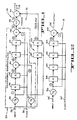
- Figure 1 is a functional block diagram of a digital filter derived from the prior art, which includes the transversal bandpass filter 20 shown within the dashed line.
- Figure 2 is a functional block diagram of a digital all-pass filter 18 typical of the present invention, wherein the entire chrominance inversion process is performed within an in-line series of delays corresponding to the composite signal path.
- the structures depicting the filters 16, 18 represent the functions of the elements shown, as well as the corresponding electronic components.
- Filter 20 is typical of present DOC bandpass filters employed to separate chrominance components from luminance components, as described in U.S. Patent US ⁇ A ⁇ 4,251,831 of previous mention.
- FIG 1 also shows, outside the dashed line, the components required to convert the filter20 into an all-pass filter, designated herein the filter 16.
- the all-pass filter 18 of the invention is much simpler in configuration than the filter 16, the former filter provides an output response identical to the latter.
- the filter 16 of Figure 1 includes the transversal bandpass filter 20, coupled to means 24 for multiplying the component signal by two and re-combining it with the delayed input signal.
- the filter 20 and means 24 define a first path through which the chrominance component is processed.
- Delay equalizing means 22 defines a second path through which the composite signal is processed, and subsequently added back in the adder of means 24.
- the filter 16 includes an input line 26 and an output line 28.
- the all-pass filter 18 of Figure 2 includes similarly an input line 26' and an output line 28'.
- a clock signal used to clock the various components in both filter circuits is supplied via respective clock lines 30, 30' in filters 16, 18 and may comprise, for example, a multiple of the reference chrominance subcarrier (for example, 4Fsc): a timing signal conventionally used in color television systems.
- a multiple of the reference chrominance subcarrier for example, 4Fsc
- the signal supplied to inputs 26, 26' is an impulse function employed herein to illustrate the operation of the filters, and conventionally comprises an infinite series of digital "0" samples, followed at one point in time by a digital "1" sample, which is followed in turn by another infinite series of digital "0" samples.
- the impulse function on input 26 is supplizd to a weight function of -1/4 indicated herein at 32, along a first signal path, and to a weight function of 1/2 indicated at 34, along a second signal path.
- the "output" of weight function 32 comprises point 1 in the circuit and is coupled to the input of a first delay 36.
- the delays each provide a time delay of one clock sample.
- the delay 36 thence is coupled to a second delay 38, whose output comprises point 2 in the circuit.
- the output of delay 38 is supplied to one input of a first adder 40, which is configured at its second input to define the weight function 34, wherein the second input corresponds to point 3 of the filter.
- the output of the adder 40 is the sum of the values at points 2 and 3 and, in turn, is point 4 in the filter circuit.
- Adder 40 is coupled to a third delay 42, whose output is supplied to a fourth delay 44.
- the output of delay 44 comprises point 5 in the circuit and is supplied to one input of a second adder 46, whose second input is configured to define the weight function 32.
- the output of the adder 46 is the sum of the values at points 5 and 1, and constitutes a component signal of a composite signal input; that is, is the chrominance component signal at point 6 of the circuit if a composite color video signal were being processed by the filter.
- the component is applied to a times-two multiplier 48, which multiplies the component by two.
- the output of multiplier 48 is supplied as point 7 to the negative input of an adder 50, which operates as a subtractor device.
- the output of the adder 50 corresponds to the subtraction of the value at point 7 from the value at a point 8, and is the output 28 of the filter 16 of Figure 1. With the impulse function as an input, the output is an impulse response function.
- the impulse function on input 26 is also supplied to a delay equalizing delay 52 on a third signal path, and thence is coupled to another delay 54.
- the two delays of path three are equal to the delay caused by the delays in the first path of filter 20.
- the output of delay 54 comprises the point 8 in the circuit and is supplied to the positive input of the adder 50.
- the identical impulse function is provided on input 26' to a weight function of 1/2, indicated herein by numerical 56.
- the "output" of the weight function 56 corresponds to point 1' which, in turn corresponds to point 1 of Figure 1.
- Point 1' defines the input to a first delay 58 of a delay means.
- the output of delay 58 is supplied to a delay 60, and thence to a third delay 62.
- the latter supplies an output to a fourth delay 64, whose output comprises point 2' corresponding to the point 5 of filter 16 of Figure 1.
- the output of delay 64 is coupled to one input of an adder 66, whose output is the filter 18 output 28' corresponding to the output 28 of Figure 1.
- the input signal weighted by 1/2 via weight function 56, is also coupled directed to the second input of adder 66, and corresponds to point 1'.
- the delays 58 ⁇ 64 define the delay means of previous mention, and are clocked by the clock on line 30'.
- the impulse function is clocked through the delays, with each providing a delay of one clock sample, such as previously described in Figure 1.
- a single weighting means 56 is employed to provide at its output a weighted representation of its input, that is coupled to two different locations along the composite signal path between the input 26' of the filter 18 and the input of the adder or summing means 40.
- One of the two locations is the input to the first delay 58 of the cascaded delay means 58 ⁇ 64 and the other of the two locations is the input to the adder 66.
- the weighting means 56 includes two identical signal weighting devices.
- one signal weighting device with a weight function of 1/2 is coupled in the first composite signal path between the junction proximate the input 26' of the filter 18 and the input of the first delay 58 of the cascaded delay means 58 ⁇ 64.
- the second signal weighting device also with a weight function of 1/2, is coupled in the second composite signal path between the junction and the input of the adder 66.
- the weighting means 56 has one of its outputs coupled directly to the input of the adder 66 and the second of its output coupled to the input of the adder through intervening delays.
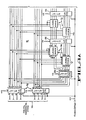
- Table 1 shows the values of the impulse response as it is clocked step-by-step through each filter's components.
- Table 1 shows the values of the impulse response as it is clocked step-by-step through each filter's components.
- the time in clock periods is depicted horizontally across Table 1, while the value of the input signal at each point, starting at the inputs and ending at the outputs of the two filters, is depicted vertically.
- the filter 16 of Figure 1 includes values at the input 26, at points 1 through 8, and at the outputs 28 thereof.
- the invention filter 18 of Figure 2 includes values at the input 26', at points 1', 2', and at the output 28'.
- the clock which may be a reference timing clock, such as 4Fsc commonly used in television systems, is applied at lines 30, 30' of the circuits and is shown across the top of Table 1 as time in successive clock periods.
- the filter 16 of Figure 1 the first four digital zeros of the input 26, on the zero, first, second and third clocks, generate all digital zeros at the points 1 through 8.
- point 1 has a value -1/4
- point 2 a has a zero
- points 3 and 4 have a 1/2
- point 5 has a zero
- point 6 has a -1/4
- point 7 has a -1/2
- point 8 has a zero
- the output has a 1/2, as a result of adder 50 subtracting -1/2 at point 7 from the zero at point 8.
- the input returns to the series of zeros, and all points 1 through 8 and the output, have zeros.
- points 1 and 3 have zeros
- points 2 and 4 have -1/4
- points 5 and 6 have +1/2
- points 7 and 8 have ones, whereby the adder 50 subtracts the sum of a +1 and +1 to provide a zero on the output 28.
- the input is zero
- the points 1 through 8 and the output are all zeros.
- the input is still zero, points 1 through 4 are zero, points 5 and 6 have -14, point 7 has -1/2 and point 8 has a zero.
- adder 50 provides an output of 1/2 as a result of subtracting a -1/2 from zero.
- all points again are at zero.
- delays 36, 38 provide two clock period delays, whereby the value that appears at point 1 on the fourth clock, is seen at point 2 two clock periods later at the sixth clock.
- the results of the impulse function may be followed through the delays, etc., via the various points in the circuit of Figure 1 in relation to the sequence of clocks supplied on line 30.
- the value at point 4 is the sum of the values at points 2 and 3 at the same clock time.
- the value at point 6 is the sum of the values at point 5 and point 1 at the same clock time.
- the digital one which was multiplied by 1/2 via weight function 56 has been delayed four clock periods by delays 58 ⁇ 64, and is added to a zero by adder 66.
- the output 28' at the eighth clock equals the sum of points 1' and 2', i.e., equals 1/2.
- the 1/2 weight function 56 is provided by shifting the bits down by one input;
- the delays 58-64 are latches, and particularly registers such as, for example, the LS273 manufactured by Texas Instruments, Inc.; and the adder 66 may be made up of 4-bit binary adders such as, for example, the LS283 manufactured by Texas Instruments. Inc., as further described in Figure 4A-4B.
- the delays 58 ⁇ 64 may be implemdnted in digital filters by any digital means for storing data, and in analog filters by analog delay lines, etc.
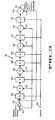
- Figure 3 depicts an alternative embodiment of the invention with added components and thus added sophistication.
- the embodiment of Figure 3 has the added advantage of providing a filter response that minimizes the amount of inverted luminance and of non-inverted chrominance in the composite video signal provided at the output of the filter. This minimization is achieved because only a band of frequencies corresponding to the range of frequency deviation of the chrominance subcarrier is inverted by the filter.
- a digital composite signal supplied to an input 70 is fed to an inverter 72, and also as one input to each of a series of adders 74, 76, 78 and 80, which together with a last stage adder 94 form a distributed summing means corresponding to the summing means 66 of the embodiment of Figure 2.
- the series of adders 74,76,78,80 and 94 are distributed along the composite signal path through the series of delays defining the delay means corresponding to the delay means of Figure 2.
- the inverted composite signal is fed to a first delay 82, and thence to a second input of the adder 74, whose output is fed to a second delay 84.
- Delay 84 is coupled to a second input of the adder 76.
- the output of the latter is supplied to a third delay 86 and thence to a fourth delay 88, whose output is fed to a second input of the adder 78.
- the output of adder 78 is supplied to a fifth delay 90 and thence to a second input of the adder 80.
- the latter provides an input to a sixth delay 92, which is coupled to a first input of an adder 94.
- the latter supplies an output 96 with a digital composite signal having an inverted component.
- the output of the inverter 72 is also coupled to a second input of the adder 94.
- the delays 82-92 are clocked via a clock signal supplied on a clock line 97, and may be a conventional reference clock as previously mentioned. As in Figure 2, the delays may be implemented by registers, latches, memories, etc., whereby the registers and adders may be the same components as previously mentioned.
- the all-pass filter does not actually separate the component signal from the composite signal at any point in the circuit, and accordingly requires fewer electronic components to implement than the transversal bandpass filters of the prior art such as shown, for example, in the U.S. Patent US ⁇ A ⁇ 4,251,831 of previous mention.
- the simplified filter accomplishes the entire processes of chrominance separation, inversion and subsequent re-combination to provide the composite signal with inverted chrominance and no change of the luminance phase and amplitude, without actually separating the component signals. It follows, the processes are achieved without the usual associated delay equalizing register and the adder devices of the prior art filters.
- the digital composite signal fed to the delay 82 and adders 74, 76, 78, 80 and 94 which perform selected weighting of the composite video signal as well as summing of delayed and undelayed composite video signal portions.
- the adders therefore define a set of distributed signal weighting devices that forms a weighting means corresponding to the weighting means 56 of the embodiment of Figure 2.
- the weighting devices or adders selectively weight the undelayed composite video signal by the weight functions -1/4 and 1/2, 1/4, 1/4, 1/2 and -1/4, respectively.
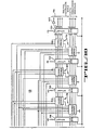
- an input terminal 70 is herein supplied with a digital composite color video signal in the form of binary 8-bit data samples, and thence to a latch 98.
- the latter herein is exemplified as a quad D-type flip-flop which converts the data from the binary number system to a 2's complement number system, to provide the minus numbers required by the filter. Use of the 2's complement system allows the circuit to do mathematical overloads within the filter without any complications.
- the latch 82 (which is exemplified herein as a hex D-type flip-flop) is coupled to those output pins on latch 98 which provide the latter with video data in inverted form and with the weight functions of -1/4 depicted in Figure 3.
- the "delay" elements of Figures 1-3 and thus the components 82-92, all are herein termed “latches” for ease of description.
- the latch 82 is coupled to the adder 74 with the bits shifted down by one to provide the 1/2 weight function depicted in Figure 3.
- the adders 76 ⁇ 80 and 94 are selectively coupled to specific output pins of the latch 98 to provide the weight functions and signs previously depicted in Figure 3.
- filter weight functions have a symmetrical relationship about the center of the filter configuration, i.e., the point between latches 86 and 88, to provide symmetrical weighting of the composite signal.
- the resulting symmetrical coefficient provides a preferred linear response of phase shift versus frequency for the all-pass filter of the invention which, in turn, assures that the inverted chrominance is accomplished while preventing an objectionable change in the luminance phase and amplitude relative to the inverted chrominance.
- the output of the adder 94 in Figure 4B is coupled to a further lach 100, which re-clocks the data samples before supplying them to the output terminal 96 as the digital composite color video signal with chrominance inverted and no change to the relative phase and amplitude of the luminance.
- the most significant bit of the sample (pin 19) is inverted via inverter 102 to convert the data from the 2's complement number system back to the binary number system.
- the invention all-pass filter contemplates further filter configuration wherein the clock rate of 4Fsc is replaced by another selected chrominance subcarrier frequency.
- the filter structure taps, or weights, delays and adders are selected to conform to the new clock frequency.
Description
- The invention relates to filters for processing composite signals, and particularly to a filter for processing of composite color video signals without separating the luminance and chrominance components forming the composite signal.
- In the processing of composite signals such as, for example, color television signals, it is commonly known to separate various signal components, such as luminance and chrominance, into separate signal paths to allow individual processing, with subsequent re-combination of the processed components into a composite signal for further use. More particularly, in the color television field, the technique of signal separation, processing and re-combination is used when performing chrominance inversion, for example, in the process commonly known as dropout compensation, used during the magnetic reproduction of video signals from magnetic tape. The corresponding dropout compensators provide compensation by replacing an incorrect or missing portion of the color television signal, commonly called a dropout, caused by an improper recording or reproduction process or by a defect in the recording medium. Thus the disturbing effects of a dropout in a television picture as seen by a viewer, are removed.
- Typical of known devices for separating a composite signal into component signals of different frequencies, are comb filters and bandpass filters. The former combine horizontal samples from two or more scan lines, while the latter employ samples from within the same line. In general, bandpass filters are designed to pass signals of selected bands of frequencies and to reject signals outside the selected bands. It follows that such bandpass filters are useful in the dropout compensators of previous mention, to provide separation of luminance and chrominance components to allow the component signal processing required when performing dropout compensation.
- By way of example, a dropout compensator and bandpass filter combination is described in U.S. Patent US―A―4,251,831 to B. Y. Kamath, assigned to the same assignee as this application, wherein a transversal bandpass filter, and dropout compensator (DOC) employing the filter, are digital circuits operating on a digitized composite color video signal. As described in the patent, the filter is a type of digital bandpass filter which selects one or more signal components of a composite signal, and particularly of a composite color video signal. The digital signal to be processed is obtained in generally known fashion; for example, by sampling the analog composite video signal utilizing a sampling clock signal which is frequency and phased locked to the selected frequency component or components to be filtered, to provide digital representations of the samples. The filter employs a combination of digital storage devices, such as registers or latches serving as signal delay devices, and arithmetic circuitry arranged and operated to provide at the filter's output, for each digitized sample received at the filter's input, a digital average representation of the values of a selected number of received samples. The number of samples averaged is selected to define a time interval which provides, in this example, a zero average value of the averaged digital sample representations corresponding to the signal component to be eliminated from the composite signal by the filter. Control of the digital storage and arithmetic means is provided by a clock signal that has a frequency which is synchronized with and equal to the frequency at which the samples are received by the filter. In situations where the composite signal is transmitted to the filter at an unpredictable and randomly varying rate, the frequency of the filter clock signal varies synchronously with the varying of receipt of the digitized samples. In situations where the digitized samples are received at a stable rate, a stable frequency clock signal is provided to control the filter.
- As typified by the filter of the above-mentioned patent, and as generally the case in bandpass filters such as those employed in dropout compensators for processing color television signals, processing of specific frequency components from a digitized composite signal is performed by first actually separating the chrominance component from the composite color video signal. Thus, if follows that a separate luminance and chrominance signal path is required to allow manipulating the chrominance prior to re-combining the luminance and chrominance, to assure proper phase of chrominance when the signal subsequently is substituted for a dropout in the color television signal.
- Thus as previously mentioned, prior dropout compensator systems have utilized digital filters in bandpass configurations to selectively process separated chrominance and luminance components. These two video components typically are processed in such a way as to synthesize video of one line from the video or one or more previous lines. In the case where the video is synthesized entirely from the previous line of video, it is apparent (in the NTSC broadcast standard) that the chrominance component must be inverted. More particularly, the processing is performed by first separating the luminance and chrominance components, inverting the chrominance component, and re-combining the two components to form the dropout compensated video. Thus, in such prior art compensation systems, the separated luminance and chrominance components are both present somewhere in the filter, and composite signal path and/or in the associated dropout compensator circuitry, and must be re-combined using some type of digital adder. In addition, some type of delay device, i.e., delay equalizing latches, must be used in the luminance path in order to equalize the signal processing times between the luminance and chrominance component signal paths.
- A preferred feature of the invention is to provide an all-pass filter of simplified configuration which synthesizes composite video from a previous video line without actually separating the luminance or chrominance components of the composite video signal.
- Another preferred feature of the invention to invert a chrominance component signal of a composite video signal being delayed without extracting the chrominance component, by the selective weighting, i.e., gain and/or attenuation values, of the composite signal in the digital filter.
- An additional feature is to provide a digitul finite impulse response, all-pass filter which inverts a selected component of a composite signal without performing a separation process.
- One possible advantage is to provide all-pass filtering without use of the usual additional equalizing delay and/or subtractor devices.
- It is known from US-A-4272785 to provide an analog filter for receiving a composite color video signal including a luminance component and a chrominance component and inverting the said chrominance component relative to the luminance component without separating the said chrominance and luminance components.
- The present invention is characterised relative thereto in that the filter is constituted as a digital transversal filter, the video signal being in the form of a succession of digital samples, the filter comprising a single chain of delay elements in a signal path extending from an input to an output, means for clocking the samples through the delay elements at a rate commensurate with the sampling rate for the said samples, signal weighting means for applying weighted versions of the video signal to at least two points of the signal path and at least one summing means in the signal path for summing a signal from the weighting means with a signal traversing the signal path, the signal weighting and the said locations being such as to provide for the filter an all-pass characteristic.
- In the digital domain it is known to provide a band-pass, digital, finite impulse-response filter arranged to receive an input color television signal which includes a luminance component and a chrominance component and is in the form of a succession of digital samples, the filter comprises a signal path including delay elements, means for clocking the samples through the delay elements at a rate commensturate with the sampling rate associated with the samples, and signal weighting means arranged to apply weighted versions of the input signal to a multiplicity of locations on the signal path. Such a filter is described hereinafter with reference to Figure 1.
- The invention is characterised relative to such a digital filter in that the locations are symmetrically disposed relative to a central location corresponding to the mean effective delay of the filter, the signal weighting and the locations are selected to provide for the filter an all-pass characteristic, and the filter is in accordance with that characteristic arranged to invert the chrominance component relative to the luminance component without sepasration of the said luminance and chrominance components while preventing an objectionable change in the phase of the luminance component relative to the chrominance component.
- A practical form of the invention is embodied in an all-pass filter which may be used, for example, in a dropout compensator system, in a slow motion operating mode system during video reproduction of a field, etc., wherein the luminance and chrominance components need not be separated in order to synthesize from previous video lines or previous fields reconstituted video with the chrominance component inverted. To this end, the all-pass filter may employ a specific modification of selected taps, i.e., weighting functions, i.e. gain and/or attenuation in the filter, to provide the synthesizing process without actually separating the luminance and chrominance components of the composite video signal. Since the all-pass filter itself performs the entire process, the need for the usual adder and delay equalizers along a separate composite signal path no longer exists, and the circuitry and the associated synthesizing process may be simplified.
- To this end, the all-pass filter provides selectively controlling the component phase inversion in selected frequency bands within a composite signal, by providing a composit color video signal path within which the chrominance component is inverted. The path may include selected delay means coupled to an input of the signal path defined by the filter for receiving and delaying the composite color video signal. Summing means to an output of the filter may sum signals received at the inputs of the summing means. A signal weighting means may be coupled to the composite signal path between the input of the signal path and the input of the summing means, for providing selected weighting factors to the composite signal at an output of the signal weighting means which is coupled to at least two different locations along the composite signal path between the input of the signal path and the input of the summing means. The weighting factor of the signal weighting means, and their point of coupling to the composite signal path, may be such as to effect inversion of the chrominance component within the composite color video signal without changing the phase and amplitude of the luminance component relative to the inverted chrominance component. The terminology "without changing the phase and amplitude of the luminance component relative to the inverted chrominance component" means in the context of the present invention that the relative phase and/or amplitude of the luminance component and chrominance component is not changed to an extent that introduces objectionable disturbance in the resulting composite video signal output by the filter with an inverted chrominance component. For broadcast television applications, it is desirable that any change in this relative phase relationship between the luminance and chrominance components be minimized so that the display of composite video signal obtained from the filter does not contain visually disturbing effects. The relative phase relationship change may be minimized in the filter by using a delay means that provides a delay substantially equal to twice the effective delay of the filter.
- As employed herein, the term "weight function" or "weighting function" is intended to correspond to tap selection, and also is intended to represent that some form of amplitude alteration is made to the composite signal by some corresponding selection of either gain and/or attenuation values. In an analog system, the weighting function is commensurate with selection of signal gain and/or signal attenuation of the analog components, as conventionally known. The weighting functions herein preferably are selected to define a symmetrical weighting of the composite signal relative to a center point in the "delay means", i.e., the plurality or series of multiple cascaded delays described hereinafter. Use of symmetrical coefficients of weighting provides a linear phase versus frequency response, which ensures that the chrominance inversion is accomplished within the composite video signal path, while preventing an objectional change in the phase and amplitude of the inverted chrominance component relative to the luminance component. The substantially symmetrical coefficients also result in the delay means delay being substantially twice the effective delay of the filter from input to output.
- In addition, the term "effective delay of the filter" is intended to mean the delay of the filter from the filter input to the filter output, i.e, the delay imparted to the composite signal fed to the filter input, upon arrival at the filter output. The term "delay means" as employed herein, refers to the actual series of delays which define the delay path of the composite color video signal, wherein the delay means delay herein preferably is twice the effective delay of the filter, given the condition of substantially symmetrical coefficients.
- As described in the U.S. Patent US-A-4,251,831, the clock rate employed herein is coherent with the composite signal and corresponds to the sampling rate in a digital system.
- Figure 1 is a block diagram functionally illustrating a prior art chrominance inverting bandpass filter with a separate chrominance component signal path, and a separate composite signal path in which delay equalizing devices must be used.
- Figure 2 is a block diagram functionally illustrating an embodiment of a digital all-pass filter of the invention combination.
- Figure 3 is a block diagram functionally illustrating an alternate embodiment of the digital all-pass filter of Figure 2.
- Figure 4A-4B is a schematic diagram of the digital all-pass filter of Figure 3.
- Figure 1 is a functional block diagram of a digital filter derived from the prior art, which includes the
transversal bandpass filter 20 shown within the dashed line. Figure 2 is a functional block diagram of a digital all-pass filter 18 typical of the present invention, wherein the entire chrominance inversion process is performed within an in-line series of delays corresponding to the composite signal path. The structures depicting thefilters Filter 20 is typical of present DOC bandpass filters employed to separate chrominance components from luminance components, as described in U.S. Patent US―A―4,251,831 of previous mention. Figure 1 also shows, outside the dashed line, the components required to convert the filter20 into an all-pass filter, designated herein thefilter 16. Although it is immediately obvious that the all-pass filter 18 of the invention is much simpler in configuration than thefilter 16, the former filter provides an output response identical to the latter. - As generally known in the filter art, it has been proven that if two digital filters are supplied with an impulse function at their inputs, and both have the same output response to that input signal, then the two filters are functionally identical. Therefore, to illustrate the advantages of the invention, the filters of Figures 1 and 2 are compared herein to show they are identical in output response, given the same input as a function of time, and therefore are identical even though the all-
pass filter 18 is much simpler. To this end, various points along the two circuits are identified, and impulse function is supplied at the input, and is followed step-by-step through both circuits to show the values of the signal at each point in the circuits. By following the two filter circuits point-by-point to their final outputs, it can be shown that the input response functions of thefilters - The
filter 16 of Figure 1 includes thetransversal bandpass filter 20, coupled to means 24 for multiplying the component signal by two and re-combining it with the delayed input signal. Thefilter 20 and means 24 define a first path through which the chrominance component is processed. Delay equalizing means 22 defines a second path through which the composite signal is processed, and subsequently added back in the adder ofmeans 24. Thefilter 16 includes aninput line 26 and an output line 28. The all-pass filter 18 of Figure 2 includes similarly an input line 26' and an output line 28'. A clock signal used to clock the various components in both filter circuits, is supplied viarespective clock lines 30, 30' infilters - The signal supplied to
inputs 26, 26', in the example used to make a comparison of the two circuits, is an impulse function employed herein to illustrate the operation of the filters, and conventionally comprises an infinite series of digital "0" samples, followed at one point in time by a digital "1" sample, which is followed in turn by another infinite series of digital "0" samples. - With reference first to the
prior art filter 16 of Figure 1, the impulse function oninput 26 is supplizd to a weight function of -1/4 indicated herein at 32, along a first signal path, and to a weight function of 1/2 indicated at 34, along a second signal path. The "output" ofweight function 32 comprisespoint 1 in the circuit and is coupled to the input of afirst delay 36. The delays each provide a time delay of one clock sample. Thedelay 36 thence is coupled to asecond delay 38, whose output comprisespoint 2 in the circuit. The output ofdelay 38 is supplied to one input of afirst adder 40, which is configured at its second input to define theweight function 34, wherein the second input corresponds to point 3 of the filter. The output of theadder 40 is the sum of the values atpoints point 4 in the filter circuit.Adder 40 is coupled to athird delay 42, whose output is supplied to afourth delay 44. The output ofdelay 44 comprisespoint 5 in the circuit and is supplied to one input of a second adder 46, whose second input is configured to define theweight function 32. - The output of the adder 46 is the sum of the values at
points multiplier 48, which multiplies the component by two. The output ofmultiplier 48 is supplied aspoint 7 to the negative input of anadder 50, which operates as a subtractor device. The output of theadder 50 corresponds to the subtraction of the value atpoint 7 from the value at apoint 8, and is the output 28 of thefilter 16 of Figure 1. With the impulse function as an input, the output is an impulse response function. - The impulse function on
input 26 is also supplied to adelay equalizing delay 52 on a third signal path, and thence is coupled to anotherdelay 54. As is well known, the two delays of path three are equal to the delay caused by the delays in the first path offilter 20. The output ofdelay 54 comprises thepoint 8 in the circuit and is supplied to the positive input of theadder 50. - Referring to Figure 2, the identical impulse function is provided on input 26' to a weight function of 1/2, indicated herein by numerical 56. The "output" of the
weight function 56 corresponds to point 1' which, in turn corresponds to point 1 of Figure 1. Point 1' defines the input to afirst delay 58 of a delay means. The output ofdelay 58 is supplied to adelay 60, and thence to athird delay 62. The latter supplies an output to afourth delay 64, whose output comprises point 2' corresponding to thepoint 5 offilter 16 of Figure 1. The output ofdelay 64 is coupled to one input of anadder 66, whose output is thefilter 18 output 28' corresponding to the output 28 of Figure 1. The input signal, weighted by 1/2 viaweight function 56, is also coupled directed to the second input ofadder 66, and corresponds to point 1'. Thedelays 58―64 define the delay means of previous mention, and are clocked by the clock on line 30'. Thus the impulse function is clocked through the delays, with each providing a delay of one clock sample, such as previously described in Figure 1. - In the embodiment of the present invention illustrated in Figure 2, a single weighting means 56 is employed to provide at its output a weighted representation of its input, that is coupled to two different locations along the composite signal path between the input 26' of the
filter 18 and the input of the adder or summingmeans 40. One of the two locations is the input to thefirst delay 58 of the cascaded delay means 58―64 and the other of the two locations is the input to theadder 66. It should be appreciated, however, the embodiment of Figure 2 could be modified so that the weighting means 56 includes two identical signal weighting devices. In such modified embodiment, one signal weighting device with a weight function of 1/2 is coupled in the first composite signal path between the junction proximate the input 26' of thefilter 18 and the input of thefirst delay 58 of the cascaded delay means 58―64. The second signal weighting device, also with a weight function of 1/2, is coupled in the second composite signal path between the junction and the input of theadder 66. In the embodiment illustrated in Figure 2 and the modified embodiment described above, the weighting means 56 has one of its outputs coupled directly to the input of theadder 66 and the second of its output coupled to the input of the adder through intervening delays. - By way of comparing the filters of Figures 1 and 2, reference is made to Table 1 herein, which shows the values of the impulse response as it is clocked step-by-step through each filter's components. Thus, for example, the time in clock periods, is depicted horizontally across Table 1, while the value of the input signal at each point, starting at the inputs and ending at the outputs of the two filters, is depicted vertically. Thus, the
filter 16 of Figure 1 includes values at theinput 26, atpoints 1 through 8, and at the outputs 28 thereof. Similarly, theinvention filter 18 of Figure 2 includes values at the input 26', at points 1', 2', and at the output 28'.
- Accordingly, by way of example only, (at least) four "0"s (zeros) are followed by a "1" (one) which is followed by five consecutive zeros to define the impulse function input. The clock, which may be a reference timing clock, such as 4Fsc commonly used in television systems, is applied at
lines 30, 30' of the circuits and is shown across the top of Table 1 as time in successive clock periods. - Considering first the
filter 16 of Figure 1, the first four digital zeros of theinput 26, on the zero, first, second and third clocks, generate all digital zeros at thepoints 1 through 8. However, when a digital one is supplied atinput 26 as at the fourth clock,point 1 has a value -1/4, point 2 a has a zero, points 3 and 4 have a 1/2,point 5 has a zero, point 6 has a -1/4,point 7 has a -1/2,point 8 has a zero, and the output has a 1/2, as a result ofadder 50 subtracting -1/2 atpoint 7 from the zero atpoint 8. - At the fifth clock, the input returns to the series of zeros, and all
points 1 through 8 and the output, have zeros. At the sixth clock, with the input at zero, points 1 and 3 have zeros, points 2 and 4 have -1/4, points 5 and 6 have +1/2, and points 7 and 8 have ones, whereby theadder 50 subtracts the sum of a +1 and +1 to provide a zero on the output 28. On the seventh clock the input is zero, thepoints 1 through 8 and the output, are all zeros. At the eighth clock the input is still zero, points 1 through 4 are zero, points 5 and 6 have -14,point 7 has -1/2 andpoint 8 has a zero. Thus adder 50 provides an output of 1/2 as a result of subtracting a -1/2 from zero. At the ninth clock all points again are at zero. - It may be seen that delays 36, 38 provide two clock period delays, whereby the value that appears at
point 1 on the fourth clock, is seen atpoint 2 two clock periods later at the sixth clock. Correspondingly, the results of the impulse function may be followed through the delays, etc., via the various points in the circuit of Figure 1 in relation to the sequence of clocks supplied online 30. Thus, for example, the value atpoint 4 is the sum of the values atpoints point 5 andpoint 1 at the same clock time. - Referring now to the all-pass filter of Figure 2, and employing the same impulse function at input 26', the same procedure may be followed at the indicated points in the circuit, i.e., points 1', 2' and the output 28'. It is readily seen that the
filter 18 is relatively simple when compared to theprior art filter 16 of Figure 1. Thus, with the digital one input at the fourth clock, point 1' has a 1/2 and point 2' and a zero, whereby the output' has a 1/2 supplied by theadder 66 when summing 1/2 and a 0. Atclock times weight function 56 has been delayed four clock periods bydelays 58―64, and is added to a zero byadder 66. Thus the output 28' at the eighth clock, equals the sum of points 1' and 2', i.e., equals 1/2. - Accordingly, by comparing the output and output' signals of the
filters - Implementation of the all-
pass filter 18 of Figure 2 is generally straightforward; the 1/2weight function 56 is provided by shifting the bits down by one input; the delays 58-64 are latches, and particularly registers such as, for example, the LS273 manufactured by Texas Instruments, Inc.; and theadder 66 may be made up of 4-bit binary adders such as, for example, the LS283 manufactured by Texas Instruments. Inc., as further described in Figure 4A-4B. Thedelays 58―64 may be implemdnted in digital filters by any digital means for storing data, and in analog filters by analog delay lines, etc. - Figure 3 depicts an alternative embodiment of the invention with added components and thus added sophistication. The embodiment of Figure 3 has the added advantage of providing a filter response that minimizes the amount of inverted luminance and of non-inverted chrominance in the composite video signal provided at the output of the filter. This minimization is achieved because only a band of frequencies corresponding to the range of frequency deviation of the chrominance subcarrier is inverted by the filter. More particularly, a digital composite signal supplied to an
input 70 is fed to aninverter 72, and also as one input to each of a series ofadders last stage adder 94 form a distributed summing means corresponding to the summing means 66 of the embodiment of Figure 2. As can be seen in Figure 3, the series ofadders first delay 82, and thence to a second input of theadder 74, whose output is fed to asecond delay 84.Delay 84 is coupled to a second input of theadder 76. The output of the latter is supplied to athird delay 86 and thence to afourth delay 88, whose output is fed to a second input of theadder 78. The output ofadder 78 is supplied to afifth delay 90 and thence to a second input of theadder 80. The latter provides an input to asixth delay 92, which is coupled to a first input of anadder 94. The latter supplies anoutput 96 with a digital composite signal having an inverted component. The output of theinverter 72 is also coupled to a second input of theadder 94. The delays 82-92 are clocked via a clock signal supplied on aclock line 97, and may be a conventional reference clock as previously mentioned. As in Figure 2, the delays may be implemented by registers, latches, memories, etc., whereby the registers and adders may be the same components as previously mentioned. - As may be seen from Figures 2 and 3, the all-pass filter does not actually separate the component signal from the composite signal at any point in the circuit, and accordingly requires fewer electronic components to implement than the transversal bandpass filters of the prior art such as shown, for example, in the U.S. Patent US―A―4,251,831 of previous mention. Thus, given a composite color video signal as an input, the simplified filter accomplishes the entire processes of chrominance separation, inversion and subsequent re-combination to provide the composite signal with inverted chrominance and no change of the luminance phase and amplitude, without actually separating the component signals. It follows, the processes are achieved without the usual associated delay equalizing register and the adder devices of the prior art filters. To this end, the digital composite signal fed to the
delay 82 andadders - Referring to Figure 4A-4B, there is depicted an implementation of the block diagram of Figure 3, wherein the configuration of delays (registers), adders and weight functions are depicted in schematic, by way of example only. Like components in the figures are similarly numbered. Thus, an
input terminal 70 is herein supplied with a digital composite color video signal in the form of binary 8-bit data samples, and thence to alatch 98. The latter herein is exemplified as a quad D-type flip-flop which converts the data from the binary number system to a 2's complement number system, to provide the minus numbers required by the filter. Use of the 2's complement system allows the circuit to do mathematical overloads within the filter without any complications. - Thus the latch 82 (which is exemplified herein as a hex D-type flip-flop) is coupled to those output pins on
latch 98 which provide the latter with video data in inverted form and with the weight functions of -1/4 depicted in Figure 3. Note that the "delay" elements of Figures 1-3 and thus the components 82-92, all are herein termed "latches" for ease of description. Thelatch 82 is coupled to theadder 74 with the bits shifted down by one to provide the 1/2 weight function depicted in Figure 3. Likewise, theadders 76―80 and 94 are selectively coupled to specific output pins of thelatch 98 to provide the weight functions and signs previously depicted in Figure 3. Note the filter weight functions have a symmetrical relationship about the center of the filter configuration, i.e., the point betweenlatches - The output of the
adder 94 in Figure 4B is coupled to afurther lach 100, which re-clocks the data samples before supplying them to theoutput terminal 96 as the digital composite color video signal with chrominance inverted and no change to the relative phase and amplitude of the luminance. The most significant bit of the sample (pin 19) is inverted viainverter 102 to convert the data from the 2's complement number system back to the binary number system. - The invention all-pass filter contemplates further filter configuration wherein the clock rate of 4Fsc is replaced by another selected chrominance subcarrier frequency. To this end, the filter structure taps, or weights, delays and adders are selected to conform to the new clock frequency.
Claims (8)
Applications Claiming Priority (2)
| Application Number | Priority Date | Filing Date | Title |
|---|---|---|---|
| US483328 | 1983-04-08 | ||
| US06/483,328 US4528598A (en) | 1983-04-08 | 1983-04-08 | Chrominance inverting all-pass filter |
Publications (3)
| Publication Number | Publication Date |
|---|---|
| EP0122096A2 EP0122096A2 (en) | 1984-10-17 |
| EP0122096A3 EP0122096A3 (en) | 1986-11-26 |
| EP0122096B1 true EP0122096B1 (en) | 1990-08-22 |
Family
ID=23919629
Family Applications (1)
| Application Number | Title | Priority Date | Filing Date |
|---|---|---|---|
| EP84302205A Expired - Lifetime EP0122096B1 (en) | 1983-04-08 | 1984-03-30 | Chrominance inverting all-pass filter |
Country Status (4)
| Country | Link |
|---|---|
| US (1) | US4528598A (en) |
| EP (1) | EP0122096B1 (en) |
| JP (1) | JPS59205889A (en) |
| DE (1) | DE3483017D1 (en) |
Families Citing this family (7)
| Publication number | Priority date | Publication date | Assignee | Title |
|---|---|---|---|---|
| US4639767A (en) * | 1983-09-08 | 1987-01-27 | Nec Corporation | Apparatus for detecting movement in a television signal based on taking ratio of signal representing frame difference to signal representing sum of picture element differences |
| KR930009881B1 (en) * | 1989-12-22 | 1993-10-12 | 삼성전자 주식회사 | Color tv signal processing circuit |
| US7085799B2 (en) * | 2000-12-07 | 2006-08-01 | Yasue Sakai | Analog filter suitable for smoothing a ΔΣ-modulated signal |
| JP2002176395A (en) * | 2000-12-07 | 2002-06-21 | Sakai Yasue | Analog filter |
| US6989779B2 (en) * | 2001-05-18 | 2006-01-24 | Rohm Co., Ltd. | Semiconductor device having DAC channels for video signals |
| US20090225877A1 (en) * | 2008-03-04 | 2009-09-10 | Francis Swarts | Method and system for characterization of filter transfer functions in ofdm systems |
| CN104380603B (en) * | 2012-05-31 | 2017-06-20 | 杜比实验室特许公司 | Low latency and low complex degree phase-shift network |
Family Cites Families (5)
| Publication number | Priority date | Publication date | Assignee | Title |
|---|---|---|---|---|
| GB1589476A (en) * | 1976-11-15 | 1981-05-13 | Rca Corp | Dropout compensator circuit |
| US4272785A (en) * | 1979-06-01 | 1981-06-09 | Rca Corporation | Defect compensation for color television |
| US4251831A (en) * | 1979-10-26 | 1981-02-17 | Kamath Bantval Y | Filter and system incorporating the filter for processing discrete samples of composite signals |
| US4376955A (en) * | 1980-02-28 | 1983-03-15 | Rca Corporation | Two dimensional adaptive dropout compensator and chroma inverter |
| JPS5873296A (en) * | 1981-10-27 | 1983-05-02 | Hitachi Ltd | Dropout compensating circuit |
-
1983
- 1983-04-08 US US06/483,328 patent/US4528598A/en not_active Expired - Lifetime
-
1984
- 1984-03-30 EP EP84302205A patent/EP0122096B1/en not_active Expired - Lifetime
- 1984-03-30 DE DE8484302205T patent/DE3483017D1/en not_active Expired - Lifetime
- 1984-04-05 JP JP59068345A patent/JPS59205889A/en active Pending
Also Published As
| Publication number | Publication date |
|---|---|
| EP0122096A2 (en) | 1984-10-17 |
| DE3483017D1 (en) | 1990-09-27 |
| EP0122096A3 (en) | 1986-11-26 |
| US4528598A (en) | 1985-07-09 |
| JPS59205889A (en) | 1984-11-21 |
Similar Documents
| Publication | Publication Date | Title |
|---|---|---|
| KR100388579B1 (en) | Luma/chroma separation filter with common delay element | |
| KR910004310B1 (en) | Digital signal separating filter | |
| US4994906A (en) | Digital luminance/chrominance separation apparatus | |
| US4464675A (en) | Low frequency digital comb filter system | |
| US4743960A (en) | Circuit for producing analog signals of primary colors of a television signal from its digital luminance and chrominance components | |
| US4456922A (en) | Reduced data rate comb filter system | |
| KR940011030B1 (en) | Signal filtering system | |
| EP0122096B1 (en) | Chrominance inverting all-pass filter | |
| EP0549174B1 (en) | Adaptive chrominance filtering control | |
| JPS6135692A (en) | Video signal processing system | |
| US6437827B1 (en) | Filtering video signals containing chrominance information | |
| JPH0646817B2 (en) | Video signal processor | |
| NL8200408A (en) | DEVICE FOR DIGITAL FILTERING OF A DIGITALIZED CHROMINANCE SIGNAL IN A TELEVISION SYSTEM WITH DIGITAL COMPONENTS. | |
| US4395729A (en) | Digital video signal processing filters with signal-to-noise enhancement | |
| US4398209A (en) | Method and apparatus for digital control of a separately coded color television signal | |
| EP0623269B1 (en) | Signal sampling | |
| JP3805043B2 (en) | Apparatus for separating a digital composite video signal into components. | |
| JP2590910B2 (en) | Digital filter | |
| JPH04318768A (en) | Nonlinear signal processor | |
| GB2153618A (en) | Processing of periodic signals | |
| JPS5887990A (en) | Digital signal isolating circuit network | |
| KR0139798B1 (en) | System for separating brightness chroma signal | |
| KR950004652Y1 (en) | Luma/chroma separation apparatus | |
| GB2150381A (en) | A signal processing filter | |
| JPH02134909A (en) | Feedback comb line filter |
Legal Events
| Date | Code | Title | Description |
|---|---|---|---|
| PUAI | Public reference made under article 153(3) epc to a published international application that has entered the european phase |
Free format text: ORIGINAL CODE: 0009012 |
|
| AK | Designated contracting states |
Designated state(s): CH DE FR GB LI NL |
|
| PUAL | Search report despatched |
Free format text: ORIGINAL CODE: 0009013 |
|
| AK | Designated contracting states |
Kind code of ref document: A3 Designated state(s): CH DE FR GB LI NL |
|
| 17P | Request for examination filed |
Effective date: 19870331 |
|
| 17Q | First examination report despatched |
Effective date: 19890502 |
|
| GRAA | (expected) grant |
Free format text: ORIGINAL CODE: 0009210 |
|
| AK | Designated contracting states |
Kind code of ref document: B1 Designated state(s): CH DE FR GB LI NL |
|
| REF | Corresponds to: |
Ref document number: 3483017 Country of ref document: DE Date of ref document: 19900927 |
|
| ET | Fr: translation filed | ||
| PLBE | No opposition filed within time limit |
Free format text: ORIGINAL CODE: 0009261 |
|
| STAA | Information on the status of an ep patent application or granted ep patent |
Free format text: STATUS: NO OPPOSITION FILED WITHIN TIME LIMIT |
|
| 26N | No opposition filed | ||
| PGFP | Annual fee paid to national office [announced via postgrant information from national office to epo] |
Ref country code: FR Payment date: 19930309 Year of fee payment: 10 |
|
| PGFP | Annual fee paid to national office [announced via postgrant information from national office to epo] |
Ref country code: GB Payment date: 19930319 Year of fee payment: 10 |
|
| PGFP | Annual fee paid to national office [announced via postgrant information from national office to epo] |
Ref country code: DE Payment date: 19930324 Year of fee payment: 10 |
|
| PGFP | Annual fee paid to national office [announced via postgrant information from national office to epo] |
Ref country code: CH Payment date: 19930325 Year of fee payment: 10 |
|
| PGFP | Annual fee paid to national office [announced via postgrant information from national office to epo] |
Ref country code: NL Payment date: 19930331 Year of fee payment: 10 |
|
| REG | Reference to a national code |
Ref country code: GB Ref legal event code: 732E |
|
| PG25 | Lapsed in a contracting state [announced via postgrant information from national office to epo] |
Ref country code: GB Effective date: 19940330 |
|
| PG25 | Lapsed in a contracting state [announced via postgrant information from national office to epo] |
Ref country code: LI Effective date: 19940331 Ref country code: CH Effective date: 19940331 |
|
| NLS | Nl: assignments of ep-patents |
Owner name: AMPEX SYSTEMS CORPORATION TE REDWOOD CITY, CALIFOR |
|
| PG25 | Lapsed in a contracting state [announced via postgrant information from national office to epo] |
Ref country code: NL Effective date: 19941001 |
|
| NLV4 | Nl: lapsed or anulled due to non-payment of the annual fee | ||
| GBPC | Gb: european patent ceased through non-payment of renewal fee |
Effective date: 19940330 |
|
| PG25 | Lapsed in a contracting state [announced via postgrant information from national office to epo] |
Ref country code: FR Effective date: 19941130 |
|
| REG | Reference to a national code |
Ref country code: CH Ref legal event code: PL |
|
| PG25 | Lapsed in a contracting state [announced via postgrant information from national office to epo] |
Ref country code: DE Effective date: 19941201 |
|
| REG | Reference to a national code |
Ref country code: FR Ref legal event code: ST |