EP0120552B1 - Conference bridge - Google Patents
Conference bridge Download PDFInfo
- Publication number
- EP0120552B1 EP0120552B1 EP84300153A EP84300153A EP0120552B1 EP 0120552 B1 EP0120552 B1 EP 0120552B1 EP 84300153 A EP84300153 A EP 84300153A EP 84300153 A EP84300153 A EP 84300153A EP 0120552 B1 EP0120552 B1 EP 0120552B1
- Authority
- EP
- European Patent Office
- Prior art keywords
- conference
- party
- bridge
- contributions
- bit
- Prior art date
- Legal status (The legal status is an assumption and is not a legal conclusion. Google has not performed a legal analysis and makes no representation as to the accuracy of the status listed.)
- Expired
Links
Images


Classifications
-
- H—ELECTRICITY
- H04—ELECTRIC COMMUNICATION TECHNIQUE
- H04M—TELEPHONIC COMMUNICATION
- H04M3/00—Automatic or semi-automatic exchanges
- H04M3/42—Systems providing special services or facilities to subscribers
- H04M3/56—Arrangements for connecting several subscribers to a common circuit, i.e. affording conference facilities
- H04M3/561—Arrangements for connecting several subscribers to a common circuit, i.e. affording conference facilities by multiplexing
Definitions
- the present invention relates to conference bridges and more particular to conference bridges for use in digital time division multiplex PCM telecommunication exchanges.
- the conference bridge conferences 8 bit PCM data channels.
- the conference bridge of the present invention has been designed for use in the electronic switching system as described in our co-pending European Patent Application No. 83304984.4 (EP-A-103437).
- the conference bridge can be configured to conference 8 bit PCM voice samples which have been encoded linearly or to A law standards or p law standards. (All 8 KHz sampling rates).
- GB-A-1498316 One conference bridge capable of conferencing 8-bit PCM encoded voice samples for use in a digital TDM-PCM exchange is disclosed in GB-A-1498316.
- each tdm sample from each party is stored in a party memory and a running total of all parties contributions is stored in an accumulator.
- the partys contribution to the last frame is subtracted from the running total, the balance of the running total being output to the party.
- the partys current contribution is then added to the balance to provide a new running total to be stored in the accumulator.
- one object of the present invention is to provide a conference bridge similar to that outlined above but in which accumulation of errors is inhibited.
- the present invention provides a conference bridge which has a party RAM which stores individual contributions to a conference and a totaliser which stores the calculated total contributions to a conference, each party contribution being subtracted from the calculated total contribution prior to outputting the total to the respective parties, the bridge including means arranged to determine time frame boundaries to cause a total stored in respect of a previous time slot to be erased and a new total calculated from each partys contribution to a subsequent time slot to be used for output.
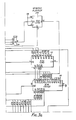
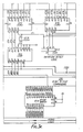
- the conference bridge 10 is equivalent to a whole shelf and hence has a shelf address within the system of Figure 1. It is addressable by the control computer (not shown ⁇ via the TDM network controller 114 and address bus ABO and data bus DBO. Data is transmitted by the bridge on the lower byte of the bus (bits 8-15) and received on the upper byte (bits 0-7)-see Figure 2.
- the exchange for security has two separate control systems A and B and a conference bridge is allocated to each of the'sides as shown. The operation of both bridges is identical.
- the Address bus command structure is of the form
- Each conference is allocated a unique channel number and each party within a conference a unique party number, the resulting seven bit address thus defines the individual contributions to a conference.
- This contribution may consist of 8 bit linearly encoded PCM voice or data samples or A law or p law encoded PCM samples. The remaining bit is used to enable an operator or other party to listen in on a conference without providing contributions to the conference. Thus enabling call monitoring functions to be performed.
- the conference bridge provides a two way connection by accumulating speech samples in the present time frame and supplying speech samples from the previous time frame's calculations.
- the output of the conference bridge in a given time frame is the algebraic sum of the previous frame's samples (for a given conference channel) less the contribution of the party receiving the output. (A time frame is 125 ⁇ s long in the system described).
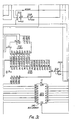
- the conference bridge must not be addressed more often than once every four time slots each time slot being 144n sec long. That is, if time slot n contains a conference bridge entry then time slots n+1, n+2, n+3 must not contain any conference bridge entry. These connection constraints are needed in order for the conference bridge to receive and transmit data onto the system data bus at the required time.
- the timing of signals can be seen from Figure 4 in which the upper set of waveforms and time slots CEC represent the timings for the Common Equipment Card-in this case the conference bridge and the lower set of waveforms and time slots represent the timings for examples for the telephony cards which require conference facilities. At time TO a shelf command to operate the conference bridge is transmitted on ABO.
- a data byte is transmitted out onto the parallel data highway and at time T2 after a short delay the data byte is received off the data highway. Also at time T1 a data byte is transmitted on the system intershelf bus on DBO 8-15 and at time T3 data is transmitted on the system shelf bus.
- a shelf slot command being given at time TO generating a slot command at time T4 which in turn generates an enable signal at time T5 causing data to be transmitted at time T6 at which time data on shelf data bus DBO bits 0-7 may be received from the conference bridge.
- the data is present on the intershelf bus.
- Bits 6 and 7 control the updown function, if the conference bridge has been 'downed' it will ignore any commands sent to it on the address bus.
- the commands sent to the bridge define the conference channel number (up to sixteen 0-15) and the party number in each conference (0-7) uniquely the order of command connections in the connection table does not matter. Thus as each party joins a conference he is merely allocated the next slot in the connection table.
- the conference bridge comprises an address header circuit 202 which defines which shelf in the system the conference bridge appears to be. As the bridge occupies a whole shelf only a shelf address is required.
- the connections within the conference bridge are normally PCM coded signals fed in parallel over paths whose width is indicated by the numerals giving the number of parallel paths.
- the output of the address header is connected to a first input of an address comparison circuit 204 which checks to see if the address bus ABO (0-15) is addressing the conference bridge.
- the address input from system address bus ABO (0-15) is latched into a latch circuit 206.
- a card enable up/down logic circuit 208 is included to enable the particular conference bridge to be enabled or disabled. In the latter case the alternative (B side) conference bridge will take over.
- the up/down logic circuit 208 is connected to enable a timing state logic circuit 210 which controls the reception and transmission timings of data onto and off the system bus.
- Timing state logic circuit 210 One output of the timing state logic circuit 210 is fed to a frame logic circuit 212 which controls the switching over at each time frame boundary of the running totals of each conference to give a total for a given time frame.
- a second output from the timing state logic circuit 210 is fed to a new frame first party logic circuit 214 which allows a first person into a conference to be written in and then every other party to be added to the conference.
- Eight bits of the output of the address latch 206 are fed to an address buffer 216.
- a first output of buffer 216 is used to identify in the new frame first party logic circuit 214 that a conference is required.
- a second output is used to initiate a decompanding PROM 218 which converts incoming 8 bit linear, A law or u iaw speech samples received from the upper byte of the system data bus DBO (bits 8-15) via latch 220 into 12 bit linear PCM signals for addition in an adder 222.
- the adder 222 produces a 15 bit output signal to a totaliser RAM 224 which calculates the total contributions for each conference as controlled by the frame logic circuit 212 and identified by the output from the address buffer 216.
- the 15 bit output from adder 222 is necessary to allow the addition of more than one 12 bit number.
- Each output of the totaliser RAM 224 is fed back to the adder 222 via a latch 226 for addition to the next parties contribution and also to an adder 228.
- Each incoming parties contribution is stored in a party RAM 230 which stores each parties contribution in the last time frame. This contribution is accessed when the conference total is output from the totaliser RAM 224 and is subtracted therefrom by inverting it in an inverter 232 and adding the two sums together in adder 228 to give an effective subtraction.
- the output of adder 228 is fed to an error detect and correct circuit 234 which detects if the remaining. total (which is equal to the sum of all the parties contributions less the addressed party's own contribution) is still greater than the maximum permitted value and if it is it forces full scale output (either positive or negative as required) to avoid any over/under flow to the companding PROM 236 which recompands the now 12 bits linear to A law, p law or to 8 bits linear.
- the output of PROM 236 is fed to a latch circuit 238 which stores the finalised PCM sample prior to transmission onto output data bus DB 0-7 via a bus driver 240.
Landscapes
- Engineering & Computer Science (AREA)
- Multimedia (AREA)
- Signal Processing (AREA)
- Telephonic Communication Services (AREA)
- Two-Way Televisions, Distribution Of Moving Picture Or The Like (AREA)
- Time-Division Multiplex Systems (AREA)
- Radio Relay Systems (AREA)
- Interconnected Communication Systems, Intercoms, And Interphones (AREA)
- Catalysts (AREA)
- Small-Scale Networks (AREA)
- Use Of Switch Circuits For Exchanges And Methods Of Control Of Multiplex Exchanges (AREA)
Abstract
Description
- The present invention relates to conference bridges and more particular to conference bridges for use in digital time division multiplex PCM telecommunication exchanges. The
conference bridge conferences 8 bit PCM data channels. - The conference bridge of the present invention has been designed for use in the electronic switching system as described in our co-pending European Patent Application No. 83304984.4 (EP-A-103437). The conference bridge can be configured to
conference 8 bit PCM voice samples which have been encoded linearly or to A law standards or p law standards. (All 8 KHz sampling rates). - One conference bridge capable of conferencing 8-bit PCM encoded voice samples for use in a digital TDM-PCM exchange is disclosed in GB-A-1498316. In the system of GB-A-1498316, each tdm sample from each party is stored in a party memory and a running total of all parties contributions is stored in an accumulator.
- On output to a party, the partys contribution to the last frame is subtracted from the running total, the balance of the running total being output to the party. The partys current contribution is then added to the balance to provide a new running total to be stored in the accumulator.
- One problem with a system using a continuously updated total is that any noise or other error inserted into the total remains present throughout the conference and any errors will be cumulative. Such accumulated errors may lead to a gradual degradation of the quality of a conference as it progresses.
- Accordingly, one object of the present invention is to provide a conference bridge similar to that outlined above but in which accumulation of errors is inhibited.
- Therefore the present invention provides a conference bridge which has a party RAM which stores individual contributions to a conference and a totaliser which stores the calculated total contributions to a conference, each party contribution being subtracted from the calculated total contribution prior to outputting the total to the respective parties, the bridge including means arranged to determine time frame boundaries to cause a total stored in respect of a previous time slot to be erased and a new total calculated from each partys contribution to a subsequent time slot to be used for output.
- A conference bridge in accordance with the present invention will now be described, by way of example with reference to the accompanying drawings in which:-
- Figure 1 shows the electronic switching system shown in the above co-pending application and including a conference bridge according to the present invention,
- Figure 2 shows in block diagrammatic form a conference bridge according to the present invention,
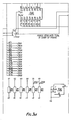
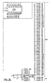
- Figure 3 shows the circuit of Figure 2 in greater detail and,
- Figure 4 shows an exemplary generalised timing system for a conference bridge of Figure 2.
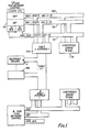
- With reference to Figure 1, the
conference bridge 10 is equivalent to a whole shelf and hence has a shelf address within the system of Figure 1. It is addressable by the control computer (not shown} via theTDM network controller 114 and address bus ABO and data bus DBO. Data is transmitted by the bridge on the lower byte of the bus (bits 8-15) and received on the upper byte (bits 0-7)-see Figure 2. - In the telephone system such as described in the above co-pending Application the exchange for security has two separate control systems A and B and a conference bridge is allocated to each of the'sides as shown. The operation of both bridges is identical.
- The Address bus command structure is of the form

- 1) Shelf address
- 2) Up/down control
- 3) Conference channel number
- 4) Conference Party number
- 5) Transmit only. Function Control.
- See timing diagram for detailed timings.
- Each conference is allocated a unique channel number and each party within a conference a unique party number, the resulting seven bit address thus defines the individual contributions to a conference. This contribution may consist of 8 bit linearly encoded PCM voice or data samples or A law or p law encoded PCM samples. The remaining bit is used to enable an operator or other party to listen in on a conference without providing contributions to the conference. Thus enabling call monitoring functions to be performed.
- The conference bridge provides a two way connection by accumulating speech samples in the present time frame and supplying speech samples from the previous time frame's calculations. The output of the conference bridge in a given time frame is the algebraic sum of the previous frame's samples (for a given conference channel) less the contribution of the party receiving the output. (A time frame is 125 µs long in the system described).
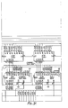
- The conference bridge must not be addressed more often than once every four time slots each time slot being 144n sec long. That is, if time slot n contains a conference bridge entry then time slots n+1, n+2, n+3 must not contain any conference bridge entry. These connection constraints are needed in order for the conference bridge to receive and transmit data onto the system data bus at the required time. The timing of signals can be seen from Figure 4 in which the upper set of waveforms and time slots CEC represent the timings for the Common Equipment Card-in this case the conference bridge and the lower set of waveforms and time slots represent the timings for examples for the telephony cards which require conference facilities. At time TO a shelf command to operate the conference bridge is transmitted on ABO. At time T1 a data byte is transmitted out onto the parallel data highway and at time T2 after a short delay the data byte is received off the data highway. Also at time T1 a data byte is transmitted on the system intershelf bus on DBO 8-15 and at time T3 data is transmitted on the system shelf bus.
- For the telephony card a similar set of timings is required with a shelf slot command being given at time TO generating a slot command at time T4 which in turn generates an enable signal at time T5 causing data to be transmitted at time T6 at which time data on shelf data bus DBO bits 0-7 may be received from the conference bridge. At time T1 the data is present on the intershelf bus.
- Thus it may be seen that in a telephone exchange system correct synchronisation is necessary to ensure that data (voice samples) are received by the conference bridge at the correct time and that sufficient time is allowed to enable the conferencing to be carried out prior to the receipt of the conferenced signals by each subscriber associated with a telephony card.
-
Bits 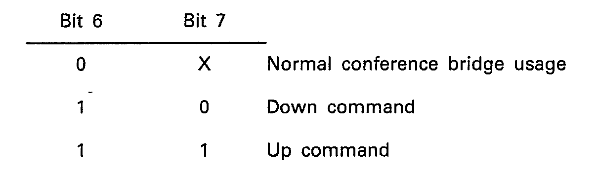
- Because the commands sent to the bridge define the conference channel number (up to sixteen 0-15) and the party number in each conference (0-7) uniquely the order of command connections in the connection table does not matter. Thus as each party joins a conference he is merely allocated the next slot in the connection table.
- If the speech samples in any conference channel on addition cause overflow to occur then the output is forced to plus or minus full scale.
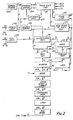
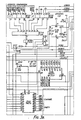
- With reference now to Figure 2 the conference bridge comprises an
address header circuit 202 which defines which shelf in the system the conference bridge appears to be. As the bridge occupies a whole shelf only a shelf address is required. The connections within the conference bridge are normally PCM coded signals fed in parallel over paths whose width is indicated by the numerals giving the number of parallel paths. - The output of the address header is connected to a first input of an
address comparison circuit 204 which checks to see if the address bus ABO (0-15) is addressing the conference bridge. The address input from system address bus ABO (0-15) is latched into alatch circuit 206. A card enable up/downlogic circuit 208 is included to enable the particular conference bridge to be enabled or disabled. In the latter case the alternative (B side) conference bridge will take over. - The up/
down logic circuit 208 is connected to enable a timingstate logic circuit 210 which controls the reception and transmission timings of data onto and off the system bus. - One output of the timing
state logic circuit 210 is fed to aframe logic circuit 212 which controls the switching over at each time frame boundary of the running totals of each conference to give a total for a given time frame. - A second output from the timing
state logic circuit 210 is fed to a new frame firstparty logic circuit 214 which allows a first person into a conference to be written in and then every other party to be added to the conference. - Eight bits of the output of the
address latch 206 are fed to anaddress buffer 216. A first output ofbuffer 216 is used to identify in the new frame firstparty logic circuit 214 that a conference is required. A second output is used to initiate adecompanding PROM 218 which converts incoming 8 bit linear, A law or u iaw speech samples received from the upper byte of the system data bus DBO (bits 8-15) vialatch 220 into 12 bit linear PCM signals for addition in anadder 222. Theadder 222 produces a 15 bit output signal to atotaliser RAM 224 which calculates the total contributions for each conference as controlled by theframe logic circuit 212 and identified by the output from theaddress buffer 216. - The 15 bit output from
adder 222 is necessary to allow the addition of more than one 12 bit number. Each output of thetotaliser RAM 224 is fed back to theadder 222 via alatch 226 for addition to the next parties contribution and also to anadder 228. - Each incoming parties contribution is stored in a
party RAM 230 which stores each parties contribution in the last time frame. This contribution is accessed when the conference total is output from thetotaliser RAM 224 and is subtracted therefrom by inverting it in aninverter 232 and adding the two sums together inadder 228 to give an effective subtraction. - The output of
adder 228 is fed to an error detect andcorrect circuit 234 which detects if the remaining. total (which is equal to the sum of all the parties contributions less the addressed party's own contribution) is still greater than the maximum permitted value and if it is it forces full scale output (either positive or negative as required) to avoid any over/under flow to thecompanding PROM 236 which recompands the now 12 bits linear to A law, p law or to 8 bits linear. The output ofPROM 236 is fed to alatch circuit 238 which stores the finalised PCM sample prior to transmission onto output data bus DB 0-7 via abus driver 240.
Claims (3)
Priority Applications (1)
| Application Number | Priority Date | Filing Date | Title |
|---|---|---|---|
| AT84300153T ATE31135T1 (en) | 1983-01-18 | 1984-01-11 | CONFERENCE BRIDGE. |
Applications Claiming Priority (2)
| Application Number | Priority Date | Filing Date | Title |
|---|---|---|---|
| GB8301323 | 1983-01-18 | ||
| GB838301323A GB8301323D0 (en) | 1983-01-18 | 1983-01-18 | Conference bridge |
Publications (2)
| Publication Number | Publication Date |
|---|---|
| EP0120552A1 EP0120552A1 (en) | 1984-10-03 |
| EP0120552B1 true EP0120552B1 (en) | 1987-11-25 |
Family
ID=10536505
Family Applications (1)
| Application Number | Title | Priority Date | Filing Date |
|---|---|---|---|
| EP84300153A Expired EP0120552B1 (en) | 1983-01-18 | 1984-01-11 | Conference bridge |
Country Status (12)
| Country | Link |
|---|---|
| EP (1) | EP0120552B1 (en) |
| JP (1) | JPS59189766A (en) |
| AT (1) | ATE31135T1 (en) |
| AU (1) | AU563083B2 (en) |
| CA (1) | CA1223324A (en) |
| DE (1) | DE3467844D1 (en) |
| DK (1) | DK22384A (en) |
| GB (1) | GB8301323D0 (en) |
| IE (1) | IE55082B1 (en) |
| NO (1) | NO160560C (en) |
| NZ (1) | NZ206836A (en) |
| ZA (1) | ZA84251B (en) |
Family Cites Families (5)
| Publication number | Priority date | Publication date | Assignee | Title |
|---|---|---|---|---|
| CA1027265A (en) * | 1975-04-23 | 1978-02-28 | Alan S.J. Chapman | Method and apparatus for establishing a plurality of simultaneous conferences in a pcm switching system |
| FR2310669A1 (en) * | 1975-05-07 | 1976-12-03 | Labo Cent Telecommunicat | MULTIPLE CONNECTION DEVICE FOR TIME-DISTRIBUTED DIGITAL SWITCHING CENTER |
| FR2334244A1 (en) * | 1975-12-04 | 1977-07-01 | Labo Cent Telecommunicat | Simultaneous multi subscriber PCM circuit - reduces computation time using sequential addition and subtraction operations at constant rate |
| JPS5474610A (en) * | 1977-11-28 | 1979-06-14 | Oki Electric Ind Co Ltd | Meeting communication system |
| JPS5528608A (en) * | 1978-08-21 | 1980-02-29 | Toshiba Corp | Conference operation system |
-
1983
- 1983-01-18 GB GB838301323A patent/GB8301323D0/en active Pending
-
1984
- 1984-01-11 DE DE8484300153T patent/DE3467844D1/en not_active Expired
- 1984-01-11 AT AT84300153T patent/ATE31135T1/en not_active IP Right Cessation
- 1984-01-11 EP EP84300153A patent/EP0120552B1/en not_active Expired
- 1984-01-11 AU AU23211/84A patent/AU563083B2/en not_active Ceased
- 1984-01-12 ZA ZA84251A patent/ZA84251B/en unknown
- 1984-01-12 NO NO840105A patent/NO160560C/en unknown
- 1984-01-13 NZ NZ206836A patent/NZ206836A/en unknown
- 1984-01-17 CA CA000445405A patent/CA1223324A/en not_active Expired
- 1984-01-17 IE IE92/84A patent/IE55082B1/en unknown
- 1984-01-18 DK DK22384A patent/DK22384A/en not_active Application Discontinuation
- 1984-01-18 JP JP59006991A patent/JPS59189766A/en active Pending
Also Published As
| Publication number | Publication date |
|---|---|
| JPS59189766A (en) | 1984-10-27 |
| DK22384A (en) | 1984-07-19 |
| CA1223324A (en) | 1987-06-23 |
| EP0120552A1 (en) | 1984-10-03 |
| NO160560B (en) | 1989-01-16 |
| ZA84251B (en) | 1984-09-26 |
| NZ206836A (en) | 1987-09-30 |
| AU563083B2 (en) | 1987-06-25 |
| AU2321184A (en) | 1984-07-19 |
| GB8301323D0 (en) | 1983-02-16 |
| DE3467844D1 (en) | 1988-01-07 |
| NO840105L (en) | 1984-07-19 |
| ATE31135T1 (en) | 1987-12-15 |
| DK22384D0 (en) | 1984-01-18 |
| IE840092L (en) | 1984-07-18 |
| IE55082B1 (en) | 1990-05-23 |
| NO160560C (en) | 1989-04-26 |
Similar Documents
| Publication | Publication Date | Title |
|---|---|---|
| US4577310A (en) | Station interface for digital electronic telephone switching system having centralized digital audio processor | |
| US4109111A (en) | Method and apparatus for establishing conference calls in a time division multiplex pulse code modulation switching system | |
| US4224688A (en) | Digital conference circuit | |
| US4301531A (en) | Three-party conference circuit for digital time-division-multiplex communication systems | |
| US5070524A (en) | Telephone system | |
| US4656625A (en) | Switching system having capability for telecommunication conferences | |
| CA1189205A (en) | Demultiplexer circuit | |
| US4416007A (en) | Digital conferencing method and arrangement | |
| US4606021A (en) | Digital conference circuit | |
| GB1529106A (en) | Method and apparatus for establishing a plurality of simultaneous conferences in a pcm switching system | |
| CA1075384A (en) | Conferencing arrangement for use in a pcm system | |
| US4195206A (en) | Path test apparatus and method | |
| EP0120552B1 (en) | Conference bridge | |
| US4472798A (en) | Telecommunication path substitution arrangement | |
| GB2134751A (en) | Conference bridge | |
| CA1191630A (en) | Pcm conference circuit | |
| US4225956A (en) | Multiplex conference bridge | |
| US4644530A (en) | Instant speaker algorithm for digital conference bridge | |
| US4133980A (en) | Data pulse register/sender for a TDM switching system | |
| CA1151327A (en) | Digital conference circuit and method | |
| USRE31814E (en) | Three-party conference circuit for digital time-division-multiplex communication systems | |
| DE3107671A1 (en) | DIGITAL TELECOMMUNICATION CONTROL DEVICE | |
| IL104106A (en) | Method of transmission of tele-communication signals | |
| CA1232663A (en) | Instant speaker algorithm for digital conference bridge | |
| CA1159540A (en) | Digital concentrator for use with a digital telephone office |
Legal Events
| Date | Code | Title | Description |
|---|---|---|---|
| PUAI | Public reference made under article 153(3) epc to a published international application that has entered the european phase |
Free format text: ORIGINAL CODE: 0009012 |
|
| AK | Designated contracting states |
Designated state(s): AT BE CH DE FR IT LI LU NL SE |
|
| 17P | Request for examination filed |
Effective date: 19850311 |
|
| 17Q | First examination report despatched |
Effective date: 19860228 |
|
| GRAA | (expected) grant |
Free format text: ORIGINAL CODE: 0009210 |
|
| AK | Designated contracting states |
Kind code of ref document: B1 Designated state(s): AT BE CH DE FR IT LI LU NL SE |
|
| REF | Corresponds to: |
Ref document number: 31135 Country of ref document: AT Date of ref document: 19871215 Kind code of ref document: T |
|
| ITF | It: translation for a ep patent filed | ||
| REF | Corresponds to: |
Ref document number: 3467844 Country of ref document: DE Date of ref document: 19880107 |
|
| PG25 | Lapsed in a contracting state [announced via postgrant information from national office to epo] |
Ref country code: LU Free format text: LAPSE BECAUSE OF NON-PAYMENT OF DUE FEES Effective date: 19880131 |
|
| ET | Fr: translation filed | ||
| PLBI | Opposition filed |
Free format text: ORIGINAL CODE: 0009260 |
|
| 26 | Opposition filed |
Opponent name: SIEMENS AKTIENGESELLSCHAFT, BERLIN UND MUENCHEN Effective date: 19880825 |
|
| NLR1 | Nl: opposition has been filed with the epo |
Opponent name: SIEMENS AKTIENGESELLSCHAFT |
|
| PGFP | Annual fee paid to national office [announced via postgrant information from national office to epo] |
Ref country code: AT Payment date: 19890111 Year of fee payment: 6 |
|
| PGFP | Annual fee paid to national office [announced via postgrant information from national office to epo] |
Ref country code: FR Payment date: 19890112 Year of fee payment: 6 |
|
| PGFP | Annual fee paid to national office [announced via postgrant information from national office to epo] |
Ref country code: SE Payment date: 19890116 Year of fee payment: 6 Ref country code: CH Payment date: 19890116 Year of fee payment: 6 |
|
| PGFP | Annual fee paid to national office [announced via postgrant information from national office to epo] |
Ref country code: BE Payment date: 19890125 Year of fee payment: 6 |
|
| ITTA | It: last paid annual fee | ||
| PGFP | Annual fee paid to national office [announced via postgrant information from national office to epo] |
Ref country code: NL Payment date: 19890131 Year of fee payment: 8 Ref country code: DE Payment date: 19890131 Year of fee payment: 6 |
|
| PGFP | Annual fee paid to national office [announced via postgrant information from national office to epo] |
Ref country code: LU Payment date: 19890220 Year of fee payment: 6 |
|
| RDAG | Patent revoked |
Free format text: ORIGINAL CODE: 0009271 |
|
| STAA | Information on the status of an ep patent application or granted ep patent |
Free format text: STATUS: PATENT REVOKED |
|
| 27W | Patent revoked |
Effective date: 19890909 |
|
| REG | Reference to a national code |
Ref country code: CH Ref legal event code: PL |
|
| NLR2 | Nl: decision of opposition | ||
| BERE | Be: lapsed |
Owner name: PLESSEY OVERSEAS LTD Effective date: 19900131 |
|
| EUG | Se: european patent has lapsed |
Ref document number: 84300153.8 |