EP0118309B1 - Semi conductor device and starter circuit for a fluorescent tube lamp, provided with such a semi conductor device - Google Patents
Semi conductor device and starter circuit for a fluorescent tube lamp, provided with such a semi conductor device Download PDFInfo
- Publication number
- EP0118309B1 EP0118309B1 EP84301451A EP84301451A EP0118309B1 EP 0118309 B1 EP0118309 B1 EP 0118309B1 EP 84301451 A EP84301451 A EP 84301451A EP 84301451 A EP84301451 A EP 84301451A EP 0118309 B1 EP0118309 B1 EP 0118309B1
- Authority
- EP
- European Patent Office
- Prior art keywords
- region
- thyristor
- circuit
- tube
- current
- Prior art date
- Legal status (The legal status is an assumption and is not a legal conclusion. Google has not performed a legal analysis and makes no representation as to the accuracy of the status listed.)
- Expired - Lifetime
Links
- 239000007858 starting material Substances 0.000 title claims description 29
- 239000004065 semiconductor Substances 0.000 title claims description 26
- 230000015556 catabolic process Effects 0.000 claims description 8
- 230000001939 inductive effect Effects 0.000 claims description 8
- 230000007704 transition Effects 0.000 claims description 6
- 230000001419 dependent effect Effects 0.000 claims description 3
- 239000012535 impurity Substances 0.000 claims description 3
- 239000000463 material Substances 0.000 claims description 3
- 238000000034 method Methods 0.000 claims description 3
- 238000001465 metallisation Methods 0.000 claims description 2
- 239000003990 capacitor Substances 0.000 description 32
- 239000004020 conductor Substances 0.000 description 21
- 238000010586 diagram Methods 0.000 description 8
- 230000035945 sensitivity Effects 0.000 description 6
- 230000000694 effects Effects 0.000 description 5
- 230000008901 benefit Effects 0.000 description 3
- 238000010276 construction Methods 0.000 description 3
- 238000010304 firing Methods 0.000 description 3
- 230000001172 regenerating effect Effects 0.000 description 3
- 230000002441 reversible effect Effects 0.000 description 3
- 230000001960 triggered effect Effects 0.000 description 3
- 230000009471 action Effects 0.000 description 2
- 238000010438 heat treatment Methods 0.000 description 2
- OAICVXFJPJFONN-UHFFFAOYSA-N Phosphorus Chemical compound [P] OAICVXFJPJFONN-UHFFFAOYSA-N 0.000 description 1
- 230000008859 change Effects 0.000 description 1
- 239000011248 coating agent Substances 0.000 description 1
- 238000000576 coating method Methods 0.000 description 1
- 230000003111 delayed effect Effects 0.000 description 1
- 238000009792 diffusion process Methods 0.000 description 1
- 238000009499 grossing Methods 0.000 description 1
- 238000005468 ion implantation Methods 0.000 description 1
- 150000002500 ions Chemical class 0.000 description 1
- 230000001151 other effect Effects 0.000 description 1
- 230000002028 premature Effects 0.000 description 1
- 229910052710 silicon Inorganic materials 0.000 description 1
- 239000010703 silicon Substances 0.000 description 1
- 230000002459 sustained effect Effects 0.000 description 1
- 238000004804 winding Methods 0.000 description 1
Images


Classifications
-
- H—ELECTRICITY
- H05—ELECTRIC TECHNIQUES NOT OTHERWISE PROVIDED FOR
- H05B—ELECTRIC HEATING; ELECTRIC LIGHT SOURCES NOT OTHERWISE PROVIDED FOR; CIRCUIT ARRANGEMENTS FOR ELECTRIC LIGHT SOURCES, IN GENERAL
- H05B41/00—Circuit arrangements or apparatus for igniting or operating discharge lamps
- H05B41/02—Details
- H05B41/04—Starting switches
- H05B41/042—Starting switches using semiconductor devices
- H05B41/044—Starting switches using semiconductor devices for lamp provided with pre-heating electrodes
- H05B41/046—Starting switches using semiconductor devices for lamp provided with pre-heating electrodes using controlled semiconductor devices
Definitions
- This invention relates to a semiconductor device as set forth in the preamble of claim 1 suitably for use in a starter circuit for a fluorescent tube lamp.
- the invention also relates to such a starter circuit and a lamp fitting incorporating the circuit.
- Fluorescent tubes are lamps which produce light by means of an electrical discharge in a gas which excites a phosphor coating on the tube.
- the impedance of the tube When in operation, the impedance of the tube is negative and therefore requires an added series impedance so that the operation is stable.
- the series impedance is usually chosen to be reactive so as to reduce power losses.
- the "running" voltage is between 20 and 60 per cent of the nominal AC supply voltage, the remainder of that voltage being dropped across the added series impedance.
- the purpose of a starting circuit is to strike the discharge in the tube and the voltage required to achieve this is higher than the running voltage and depends on the age of the tube, its operational environment and the length of time for which striking voltage is applied. Tubes have heated cathodes which provide a source of ions and electrons for the discharge and reduce the magnitude of the voltage required to strike the tube. It is possible to strike a tube when the cathodes are cold but the striking voltage/time requirement is usually beyond the capability of conventional starting circuits; and, in any case, the cold striking of a tube tends to shorten its life.
- a well-known circuit for achieving this includes a glow tube switch which is used to complete a series circuit including the ballast series impedance and the two cathode heaters, the switch itself being connected between the two cathode heaters.
- this strip When sufficiently hot, this strip closes some switch contacts which short-circuit the glow tube and cause the cathode heaters to be heated by the supply current. After a certain period of time the bimetallic strip cools allowing the switch to open again which interrupts the heater current and causes the ballast impedance, which is usually an inductor, to produce an e.m.f. in addition to the supply voltage which is usually sufficient to strike the tube. If the tube does not strike, the glow tube switch will repeat its attempt to strike it as described above. After the tube has struck insufficient voltage is applied to the glow tube for the discharge to be set up in it and the starter remains quiescent.
- the main problems with the glow tube switch as described above are that the actual time of opening of the switch is random relative to the supply voltage so that the actual e.m.f. applied to the tube in an attempt to strike it is frequently insufficient so that the striking of the tube is delayed and it is preceded by an unpleasant series of flashes. Furthermore, the performances of the glow tube starters are very variable which can result in unreliable operation in some instances. In addition, the life expectancy of the glow tube switch is unpredictable. Moreover, the continued attempts to strike a faulty tube by such a switch can be very annoying.
- a semiconductor device having a thyristor formed in a body of semiconductor material of a first conductivity type, the body providing a first region of the thyristor, the device including second and third regions, of a second conductivity type opposite to the first conductivity type, respectively formed in the opposite major faces of the body, and a fourth region, of the first conductivity type, formed in the second region, the device further including a fifth region, of the second conductivity type, alongside the second region and sixth region, of the first conductivity type in the fifth region, a connection being provided from.
- the sixth region to the second region, characterised in that the third region covers at least those parts of the major face of the body in which it is formed which lie opposite the second and fifth regions in the other major face of the body, so that the device includes an auxiliary thyristor and a main thyristor in Darlington connection, the main thyristor being formed by the fourth region, the second region, the first region and the third region, and the auxiliary thyristor being formed by the sixth region, the fifth region, the first region and the third region, parts of the second region penetrate the fourth region to reach the major face of the body, and metallisation providing a connection to the fourth region causes the parts of the second region to be connected in parallel with the pn junction between the second and fourth regions, thereby causing the main thyristor to have a high holding current, a seventh region is provided, of the second conductivity type but of lower impurity concentration than the second, third and fifth regions, the seventh region covering whole of the fifth region and covering the periphery of the second region
- the invention provides a starter circuit for an a.c. energised fluorescent tube lamp having cathodes with heaters and an inductive ballast impedance in which in use the circuit is connected between the cathode heaters of the tube itself and presents a low impedance enabling the heaters to be energised during part of the starting procedure and a high impedance whilst the tube is running, the circuit including a thyristor, characterised in that the circuit includes a semiconductor device according to the above paragraph connected by its main terminals between the cathode heaters so that the transition from low impedance to high impedance of the path between the main terminals of the device occurs when the cyclically varying current through the path falls below the holding current of the main thyristor of the device, the circuit being such that in use the inductive ballast impedance stores energy corresponding substantially to the passage of the high holding current through it at the instant of the transition from low impedance to high impedance, the holding current being determined by the
- the avalanche diode clamp Since the amount of energy stored in the inductive ballast impedance at the instant of the transition from low impedance to high impedance of the controlled current path is fixed by the holding current of the main thyristor and the inductance of the impedance, and the voltage of the supply at that instant is predetermined, it follows that the use of the avalanche diode clamp will result in a pulse of known amplitude and duration being applied to the tube.
- the parameters determining the amplitude and duration of the pulse are chosen to suit the starting conditions required by the tube.
- the thyristor In order to provide for the heating of the cathodes the thyristor needs to be held in the low impedance condition for a period of preheating appropriate to the tube. This can be achieved by providing a resistive connection from the first main terminal of the semiconductor device to its control input terminal to hold it in conduction and then short-circuiting the control input terminal to the second main terminal of the device or otherwise holding the control input terminal bias sufficiently negative at the end of the preheating period so that the main thyristor switches to the high impedance condition when the current next falls below the holding value.
- the duration of the preheating period may be made inversely dependent on the preheating current so that the same starting circuit is suitable for different sizes of tube.
- the circuit may be arranged to produce only a single striking pulse before it becomes quiescent or it may produce striking pulses for a predetermined period and then become quiescent.
- the circuit includes a diode bridge rectifier circuit so that the conductive state of the semiconductor device can control the current in both phases of the a.c. supply.
- a single diode half wave rectifier may be used provided that adequate power can be applied to the cathode heaters when the semiconductor device is conducting.
- the invention also provides a lamp fixture for a fluorescent tube lamp having cathodes with heaters, the fixture further including an inductive ballast impedance connected in series between the lamp terminals and a.c. supply terminals and a starter circuit, according to the second aspect of the invention and a rectifier connected to the lamp terminals to supply a rectified voltage to the semiconductor device.
- the starter circuit is mounted in a box, so that the box and circuit together are detachable from the fixture and are of substantially the same size and shape as a conventional fluorescent lamp starter switch.
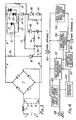
- a.c. supply terminals 1 and 2 are provided of which the terminal 1 is connected through a ballast choke 3 to one end of a cathode heater winding 4 of a fluorescent tube lamp 5.
- the terminal 2 is connected directly to an end terminal of the heater 6 of a second cathode of the tube 5.
- the other ends of the heaters 4 and 6 are connected across a diagonal of a diode bridge rectifier 7 of which the output diagonal is connected to a positive conductor 8 and a negative conductor 9.
- the positive conductor 8 is connected to the negative conductor 9 through two parallel circuits.
- a resistor 10 and a capacitor 11 are connected in series and in the other parallel circuit a semiconductor device, herein referred to as a "fluoractor" 12 is connected in series with a diode 13 and a resistor 14 connected in parallel with one another.
- the junction of the resistor 10 and the capacitor 11 is connected via a resistor 15 to the gate or control electrode of the fluoractor 12, which electrode is connected through a thyristor 16 to the negative conductor 9.
- the junction of the fluoractor 12 and the diode 13 is connected through a resistor 17 to the gate of the thyristor 16 which electrode is connected to the negative conductor 9 through a series circuit consisting of a resistor 18 and a capacitor 19.
- the fluoractor 12 is a monolithic power semiconductor structure which includes a main thyristor 20 and an auxiliary thyristor 21 with their anodes connected together.
- the cathode of the auxiliary thyristor 21 is connected to the gate of the main thyristor 20 and the gate of the auxiliary thyristor 21 acts as the gate of the fluoractor.
- a zener diode or other voltage limiting structure 22 is provided in parallel with the anode-cathode path of the main thyristor 20 which forms the controlled current path of the fluoractor 12.
- the auxiliary thyristor 21 is of conventional thyristor construction and has in effect a resistor 23 of 1 k ⁇ connected between gate and cathode.
- the main thyristor 20 has a modified construction with a number of shorting dots shorting the gate to cathode junction, the effect of which is to cause the thyristor 20 to require a particularly high current to hold it in conduction when there is no positive bias on the gate. Another effect of the shorting dots is to produce the effect that the gate is effectively shorted to the cathode of this thyristor through a resistance 24 of about 30 Q. Other effects are produced by the structure and these will be described where appropriate in the description of the operation of the circuit.
- the starter circuit consists of the components shown in Figure 1 to the right of the tube 5 and these would be included in a small cylindrical package such as that used for a conventional glow switch starter and it is intended that they would be directly replaceable items for a glow switch starter.
- the starting circuit switches to a high impedance. This is achieved in the circuit shown in Figure 1 by the flow of current through the resistors 17 and 18 which causes the capacitor 19 to be charged up.
- the preheating period for the cathodes expires the amount of charge on the capacitor 19 is sufficient to permit the junction of resistors 17 and 18 to have reached a voltage high enough to cause the thyristor 16 to become conducting, thus bringing the potential applied to the gate of the fluoractor 12 down to a voltage close to that of the negative conductor 9.
- the alternating supply is rectified by the diode bridge 7 but is not subjected to any significant smoothing, there is quite a large 100 Hz ripple superimposed on the d.c. supply with the result that the voltage which appears at the junction of the resistors 17 and 18 also contains a significant 100 Hz ripple which ensures that the time of firing of the thyristor 16 occurs near a voltage peak of the a.c. supply.
- the fluoractor 12 remains conducting as long as the current through it exceeds the holding current of the main thyristor 20. However, the current through the fluoractor 12 which is substantially in phase with the voltage across it follows a succession of half sine waves resulting from the full wave rectification of the a.c. supply.
- the above expression is approximately valid for a lagging power factor circuit; for a leading power factor circuit the expression is modified by a change of the positive sign to a negative one in the denominator so that the duration of the pulse is longer.
- the voltage V clamp is that which is available to strike the tube, it being applied across the two cathodes of the tube.
- the circuit of Figure 1 produces only a single striking pulse because once the thyristor 16 has been triggered into conduction, it remains conducting because sufficient current flows through the resistors 10 and 15 to keep in that condition and therefore the voltage applied to the gate of the fluoractor 12 remains too negative to permit it to conduct. If the striking pulse is not effective in striking the tube the a.c. power may be switched off and reapplied for a second attempt. There is no appreciable delay in the termination of the conduction of the thyristor 16 once the a.c. supply is switched off, because the charge in the capacitor 11 is rapidly reduced through the relatively low resistor 15 and the thyristor 16.
- Figure 2 shows an alternative circuit which produces a plurality of striking pulses over a controlled period after which the circuit becomes quiescent.
- Components of Figure 2 which correspond exactly to those of Figure 1 have the same reference numbers as in that Figure.
- the terminals A and B of Figure 2 correspond to those marked on the conductors 8 and 9 in Figure 1, the remainder of the circuit to the left of those terminals being exactly as shown in Figure 1.
- the controlled current path of the fluoractor 12 is connected from the positive conductor 8 through diodes 30 and 31 in series to the negative conductor 9.
- Transistors 32 and 33 are connected in a regenerative feedback circuit to act as a thyristor but the collector load of the transistor 33 takes the form of a diode-connected transistor 34 connected between the collector of the transistor 33 and the conductor 9.
- the collector of the transistor 33 is connected to the junction of the diodes 30 and 31 through a resistor 35.
- the base of the transistor 33 is connected to its emitter through a resistor 36 and that emitter is connected directly to the gate of the fluoractor 12 and through a resistor 37 to the conductor 8.
- the transistor 32 With regard to the transistor 32, its collector is connected directly to the base of the transistor 33, its emitter is connected directly to the conductor 9 and its base is connected through a resistor 38 to the collector of the transistor 33, to the conductor 9 through a capacitor 39 and to one end of a resistor 40.
- a resistor 41 and a capacitor 42 are connected in series from the conductor 8 to the conductor 9.
- the capacitor 42 is shunted by a resistor 43.
- the junction of the resistor 41 and the capacitor 42 is connected through a resistor 45 to the other end of the resistor 40 and the junction of these two resistors is connected to the conductor 9 through a capacitor 44.
- the size of the capacitor 39 is so much smaller than that of the capacitor 44 that it can be ignored during consideration of this part of the operation of the circuit; the capacitor 39 is provided to absorb spurious noise pulses which might otherwise trigger the thyristor formed by the transistors 32 and 33.
- the transistors 32 and 33 Up to this time the transistors 32 and 33 have been non-conducting, but when the voltage at the base of the transistor 32 reaches about 0.7 volts the transistors 32 and 33 become conducting with the result that the gate of the fluoractor 12 is taken to a more negative value so that the fluoractor becomes non-conducting when the current through it falls below its relatively high holding current. Because the d.c.
- the period of time necessary to build up an adequate voltage at the base of the transistor 32 to cause the thyristor formed by the transistors 32 and 33 to start conducting again is shorter than it was initially because of the residual charge stored in the capacitor 44, but as the cathodes of the tube are already heated, it is not necessary for current to be fed through the cathode heaters for the full reheat period between its striking pulses.
- the structure of the fluoractor is such that whilst it is conducting and also whilst it is clamping the voltage being applied across it, current flows out of the gate connection and this current flows through the thyristor formed by the transistors 32 and 33 to charge up not only the capacitor 44 but also the capacitor 42. Therefore, during each striking pulse the charge stored in the capacitor 42 is increased with the result that if the tube fails to strike after a few seconds sufficient charge will have been accumulated by the capacitor 42 for the voltage at the base of the transistor 32 to be high enough to hold the thyristor formed by the transistors 32 and 33 in conduction whenever a positive voltage appears at the emitter of the transistor 33. This means that the fluoractor 12 does not become conducting and the circuit assumes a quiescent state in which the charge on the capacitor 42 is sustained by current flow through the resistor 41 and the thyristor formed by the transistors 32 and 33 is continuously conducting.
- Figure 3 shows a further starter circuit according to the invention which is similar to the circuit shown in Figure 1 but which provides a plurality of striking pulses over a controlled period as does the circuit of Figure 2. Comparing Figure 3 with Figure 1, it will be seen that the capacitor shunting the thyristor 16 has been removed, the controlled path of the fluoractor 12 has been shunted by a resistor and the firing circuit in the thyristor 16 has been made more complex to provide the succession of striking pulses. The functions of the additional parts will become apparent from the following description of the operation of the circuit.
- the thyristor 16 is kept in a conducting condition by the current flowing out from the gate input of the fluoractor 12 together with the current through the resistor 10.
- the thyristor ceases conduction when the pulse voltage from the full wave rectifier 7 falls to zero and does not turn on as the next half wave begins because the voltage applied to its gate is too low.
- the cycle recommences and the capacitor 19 is recharged and the thyristor 16 is triggered again, this time at a slightly earlier time in the half cycle because of the residual charge in the capacitor 19.
- the cycle is repeated with the thyristor being turned on progressively earlier and earlier until finally the capacitor 19 is sufficiently charged that the thyristor is held conducting and the fluoractor 12 does not conduct because the voltage on its gate does not rise sufficiently.
- a benefit obtained by this progressively earlier triggering of the thyristor 16 is that the fluoractor can be turned off before the current through it has risen to the holding current so that after the striking pulse the tube receives a greater proportion of a half cycle of current through it which will assist in maintaining the discharge.
- the capacitor 19 is discharged quickly through the diodes 46, 47 and 48.
- Figures 4, 5 and 6 show details of the fluoractor 12, it being constructed as a monolithic semiconductor device.
- Figure 4 is a block diagram of the functions of the device, Figure 5 a nominal circuit diagram, and Figure 6 a diagram partly in cross-section of the device itself.
- the high power regenerative switch 100 is the main thyristor of the device and the high sensitivity regenerative trigger 101 is the auxiliary thyristor.
- the sensitivity delatch definition function 102 is performed by the shorting dots in the main thyristor and the sensitivity definition function 103 of the auxiliary thyristor is provided by the resistor connecting the gate of that thyristor to an end terminal of its controlled current path.
- the high voltage clamp function 104 is an avalanche breakdown diode formed in the construction of the main thyristor and the current mirror 105 is provided by a transistor having its collector connected to the gate input 106 of the device, which transistor is connected in parallel with one of the transistors forming the auxiliary thyristor 101.
- the controlled current path of the device is between main terminals 107 and 108.
- Figure 4 will help in understanding the functions of the elements of the circuit of Figure 5. As far as possible, the references used in Figure 4 have been used in Figure 5. The dotted outlines in Figure 5 have been numbered with the reference numbers used in Figure 4 indicating that the parts enclosed perform the functions shown in Figure 4.
- the thyristors are shown as regenerativeiy connected pairs of transistors. In the main thyristor 100, one of the transistors is shown as being composed of a plurality of transistors connected in parallel; this is partly because the transistor concerned is a high power one and partly because the resistors performing the sensitivity delatch definition function 102 of Figure 4 are distributed and respectively connect the base to the emitter of each of the transistors of the plurality.
- the device has a body 110 of N-type silicon with a region 111 of P-type conductivity formed on its lower major face. An ohmic contact is made to the region 111 and this forms the main terminal 1 of the device.
- the region 111 In the upper main face of the body 110 there are formed two regions, 112 and 113, of P-type conductivity joined by a short bridge 114 also of P-type conductivity.
- the region 112 In the region 112 is formed a further region 115 of N + conductivity to which an ohmic connection is made and provides the main terminal 2.
- the input or gate of the device is provided by an ohmic connection to the region 113.
- region 113 another region 116 of N + type conductivity is formed and this is connected by a conductive link 117 to the region 112 at a position near the bridge 114.
- the regions 112 and 113 are enclosed by a region 118 of P-type conductivity having a reduced impurity concentration; this is shown in Figure 6 as P-.
- the region 118 does not completely enclose the regions 112 and 113 but leaves uncovered the central substantially planar part 119 of the interface between the region 112 and the body 110.
- the N + type region 115 is provided with small areas 120 through which the P-type material of the region 112 still extends to the upper surface of the body 110 and the conductive connection forming the main terminal 2 is connected not only to the N + regions 115 but also to the P region 112 at the places 120. These perforations through the region 115 form the base to emitter resistors which perform the sensitivity delatch definition function 102 by causing the main thyristor to have a relatively high holding current.
- the perforations 120 through the region 115 provide the base to emitter resistors shown in Figure 5 on the main thyristor 100.
- the sensitivity definition function 103 of the auxiliary thyristor is provided by the bridge 114 through which the region 116 is connected to the region 113 so that it acts as a base to emitter resistor as shown in Figure 5.
- the current mirror transistor 105 is formed by the region 113, the body 110 and the region 111, this appearing as a separate component from part of the auxiliary thyristor 101 because the N + type region 116 is located towards one end of the region 113.
- the P- region 118 covers the corners of the PN junctions between the regions 112 and 113 and the body 110 so as to prevent premature reverse voltage breakdown in these areas.
- the reverse voltage breakdown PN junction between the region 112 and the body 110 is confined to the area 119 not covered by the P- region 118 which forms an accurately controlled avalanche diode clamp performing the function 104 shown in Figure 4.
- the region 111 is shown over the whole of the lower major face of the body 110, it need not do so provided that it covers those parts of the major face which are opposite the regions 112 and 113 in the other major face.
- the perforations 120 need not take the form shown but could be narrow slits or any other geometrical configuration providing the required resistive connection of the region 112 to the main terminal 2 distributed evenly over the area of the region 115.
- the device may be manufactured using conventional planar integrated circuit techniques including diffusion and/or ion implantation.
- starter circuits described are the fact that the timing of the pre- heat current can be quite precisely controlled so that the tube cathodes reach the optimum temperature for striking the tube and that the voltage clamping action of the fluoractor serves not only to limit the voltage stresses on the components of the circuit but also to extend the duration of the striking pulse applied to the tube which has been found to make the striking of the tube more reliable than with a shorter pulse.
- the voltage set up across the diode (13 of Fig. 1 or of Fig. 2) from which the firing voltage for the thyristor (16 of Fig. 1 or 32, 33 of Fig. 2) is built up may be arranged to be dependent on the magnitude of the cathode heater current by including a resistor in series with the diode.
- the energy in the striking pulse is accurately controlled because of the way in which it is generated.
- All of the starter circuits described above are arranged so that if the tube fails to strike after either a single striking pulse or a succession of striking pulses over a predetermined time interval the starter circuit becomes quiescent and produces no further striking pulses until it has been switched off and then on again. This is achieved by ensuring that the driving thyristor remains turned on and therefore shorting the gate of the fluoractor to ground.
- the starting circuits described have a number of advantages additional to those mentioned above.
- the same fall in temperature will effectively reduce the charging current of the pre-heat timing capacitor 19 or 44, thus automatically providing a longer pre-heat time.
- circuits described have used a full wave rectifier circuit, half wave rectification could be used instead, allowance being made for the effectively smaller heater current and the intervals between the rectified current pulses.
Landscapes
- Circuit Arrangements For Discharge Lamps (AREA)
Description
- This invention relates to a semiconductor device as set forth in the preamble of
claim 1 suitably for use in a starter circuit for a fluorescent tube lamp. The invention also relates to such a starter circuit and a lamp fitting incorporating the circuit. - Fluorescent tubes are lamps which produce light by means of an electrical discharge in a gas which excites a phosphor coating on the tube. When in operation, the impedance of the tube is negative and therefore requires an added series impedance so that the operation is stable. For AC circuits the series impedance is usually chosen to be reactive so as to reduce power losses.
- Once the tube has been struck the "running" voltage is between 20 and 60 per cent of the nominal AC supply voltage, the remainder of that voltage being dropped across the added series impedance. The purpose of a starting circuit is to strike the discharge in the tube and the voltage required to achieve this is higher than the running voltage and depends on the age of the tube, its operational environment and the length of time for which striking voltage is applied. Tubes have heated cathodes which provide a source of ions and electrons for the discharge and reduce the magnitude of the voltage required to strike the tube. It is possible to strike a tube when the cathodes are cold but the striking voltage/time requirement is usually beyond the capability of conventional starting circuits; and, in any case, the cold striking of a tube tends to shorten its life. Moreover the high voltages required for the larger tube sizes would call for correspondingly high voltage components, so that cold striking is not normally used for such tubes. It is therefore a function of starting circuits to provide a period for which current is applied to the cathodes to heat them and a well-known circuit for achieving this includes a glow tube switch which is used to complete a series circuit including the ballast series impedance and the two cathode heaters, the switch itself being connected between the two cathode heaters. When power is first supplied to the circuit, the full AC supply voltage is applied to the glow tube in which a discharge is set up and the heat of this discharge heats up a bimetallic strip. When sufficiently hot, this strip closes some switch contacts which short-circuit the glow tube and cause the cathode heaters to be heated by the supply current. After a certain period of time the bimetallic strip cools allowing the switch to open again which interrupts the heater current and causes the ballast impedance, which is usually an inductor, to produce an e.m.f. in addition to the supply voltage which is usually sufficient to strike the tube. If the tube does not strike, the glow tube switch will repeat its attempt to strike it as described above. After the tube has struck insufficient voltage is applied to the glow tube for the discharge to be set up in it and the starter remains quiescent.
- The main problems with the glow tube switch as described above are that the actual time of opening of the switch is random relative to the supply voltage so that the actual e.m.f. applied to the tube in an attempt to strike it is frequently insufficient so that the striking of the tube is delayed and it is preceded by an unpleasant series of flashes. Furthermore, the performances of the glow tube starters are very variable which can result in unreliable operation in some instances. In addition, the life expectancy of the glow tube switch is unpredictable. Moreover, the continued attempts to strike a faulty tube by such a switch can be very annoying.
- In order to overcome the above disadvantages of a glow tube starter switch certain semiconductor solutions have been proposed, but in many instances the circuits are quite complicated so that the switch cannot be manufactured as cheaply as a glow tube switch and cannot be fitted into the small cylindrical package used fqr such switches so that they cannot be regarded as an in-service replacement for the glow tube switch.
- In United States Patent Specifications Nos. 3,978,368 and 3,942,070, there are described starter circuits for fluorescent lamps using thyristors in Darlington connection. The circuits described are constructed solely from discrete components.
- In British Patent Specification No. 1,566,540, there is described a thyristor having transistors formed integrally with it for the purpose of amplifying the gating signal.
- It is an object of the present invention to provide an improved form of electronic circuit for starting a fluorescent tube lamp which overcomes the disadvantages of the semiconductor replacements for the glow tube switch.
- According to one aspect of the present invention there is provided a semiconductor device having a thyristor formed in a body of semiconductor material of a first conductivity type, the body providing a first region of the thyristor, the device including second and third regions, of a second conductivity type opposite to the first conductivity type, respectively formed in the opposite major faces of the body, and a fourth region, of the first conductivity type, formed in the second region, the device further including a fifth region, of the second conductivity type, alongside the second region and sixth region, of the first conductivity type in the fifth region, a connection being provided from. the sixth region to the second region, characterised in that the third region covers at least those parts of the major face of the body in which it is formed which lie opposite the second and fifth regions in the other major face of the body, so that the device includes an auxiliary thyristor and a main thyristor in Darlington connection, the main thyristor being formed by the fourth region, the second region, the first region and the third region, and the auxiliary thyristor being formed by the sixth region, the fifth region, the first region and the third region, parts of the second region penetrate the fourth region to reach the major face of the body, and metallisation providing a connection to the fourth region causes the parts of the second region to be connected in parallel with the pn junction between the second and fourth regions, thereby causing the main thyristor to have a high holding current, a seventh region is provided, of the second conductivity type but of lower impurity concentration than the second, third and fifth regions, the seventh region covering whole of the fifth region and covering the periphery of the second region, lying between the second and fifth regions and the body, the seventh region ensuring that avalanche breakdown of the junction between the first and second regions occurs in the substantially planar part of that junction, and there are provided first and second main terminals respectively connected to the third region and the fourth region and a control input terminal connected to the fifth region.
- " In a second aspect the invention provides a starter circuit for an a.c. energised fluorescent tube lamp having cathodes with heaters and an inductive ballast impedance in which in use the circuit is connected between the cathode heaters of the tube itself and presents a low impedance enabling the heaters to be energised during part of the starting procedure and a high impedance whilst the tube is running, the circuit including a thyristor, characterised in that the circuit includes a semiconductor device according to the above paragraph connected by its main terminals between the cathode heaters so that the transition from low impedance to high impedance of the path between the main terminals of the device occurs when the cyclically varying current through the path falls below the holding current of the main thyristor of the device, the circuit being such that in use the inductive ballast impedance stores energy corresponding substantially to the passage of the high holding current through it at the instant of the transition from low impedance to high impedance, the holding current being determined by the parts of the second region which penetrate the fourth region of the device, and the stored energy is converted to a striking pulse which is applied to the tube, the striking pulse being of a voltage limited by the avalanche breakdown of the junction between the first and second regions of the device.
- Since the amount of energy stored in the inductive ballast impedance at the instant of the transition from low impedance to high impedance of the controlled current path is fixed by the holding current of the main thyristor and the inductance of the impedance, and the voltage of the supply at that instant is predetermined, it follows that the use of the avalanche diode clamp will result in a pulse of known amplitude and duration being applied to the tube. Preferably the parameters determining the amplitude and duration of the pulse are chosen to suit the starting conditions required by the tube.
- In order to provide for the heating of the cathodes the thyristor needs to be held in the low impedance condition for a period of preheating appropriate to the tube. This can be achieved by providing a resistive connection from the first main terminal of the semiconductor device to its control input terminal to hold it in conduction and then short-circuiting the control input terminal to the second main terminal of the device or otherwise holding the control input terminal bias sufficiently negative at the end of the preheating period so that the main thyristor switches to the high impedance condition when the current next falls below the holding value. The duration of the preheating period may be made inversely dependent on the preheating current so that the same starting circuit is suitable for different sizes of tube.
- The circuit may be arranged to produce only a single striking pulse before it becomes quiescent or it may produce striking pulses for a predetermined period and then become quiescent.
- Preferably the circuit includes a diode bridge rectifier circuit so that the conductive state of the semiconductor device can control the current in both phases of the a.c. supply. Alternatively a single diode half wave rectifier may be used provided that adequate power can be applied to the cathode heaters when the semiconductor device is conducting.
- According to a third aspect the invention also provides a lamp fixture for a fluorescent tube lamp having cathodes with heaters, the fixture further including an inductive ballast impedance connected in series between the lamp terminals and a.c. supply terminals and a starter circuit, according to the second aspect of the invention and a rectifier connected to the lamp terminals to supply a rectified voltage to the semiconductor device.
- Preferably the starter circuit is mounted in a box, so that the box and circuit together are detachable from the fixture and are of substantially the same size and shape as a conventional fluorescent lamp starter switch.
- In order that the invention may be fully understood and readily carried into effect, it will now be described with reference to the accompanying drawings, of which:
- FIGURE 1 is a diagram of one example of a starter circuit;
- FIGURE 2 is a diagram of another starter circuit;
- FIGURE 3 is a diagram of a further example of a starter circuit; and
- FIGURES 4, 5 and 6 show a functional diagram, a nominal circuit diagram and a physical configuration respectively of a "fluoractor" suitable for use in the circuits of Figures 1, 2 and 3.
- Referring now to Figure 1, a.c.
supply terminals terminal 1 is connected through aballast choke 3 to one end of a cathode heater winding 4 of afluorescent tube lamp 5. Theterminal 2 is connected directly to an end terminal of theheater 6 of a second cathode of thetube 5. The other ends of theheaters positive conductor 8 and anegative conductor 9. Thepositive conductor 8 is connected to thenegative conductor 9 through two parallel circuits. In one of these parallel circuits aresistor 10 and a capacitor 11 are connected in series and in the other parallel circuit a semiconductor device, herein referred to as a "fluoractor" 12 is connected in series with adiode 13 and aresistor 14 connected in parallel with one another. The junction of theresistor 10 and the capacitor 11 is connected via aresistor 15 to the gate or control electrode of thefluoractor 12, which electrode is connected through athyristor 16 to thenegative conductor 9. The junction of thefluoractor 12 and thediode 13 is connected through aresistor 17 to the gate of thethyristor 16 which electrode is connected to thenegative conductor 9 through a series circuit consisting of aresistor 18 and acapacitor 19. - The
fluoractor 12 is a monolithic power semiconductor structure which includes amain thyristor 20 and anauxiliary thyristor 21 with their anodes connected together. The cathode of theauxiliary thyristor 21 is connected to the gate of themain thyristor 20 and the gate of theauxiliary thyristor 21 acts as the gate of the fluoractor. A zener diode or othervoltage limiting structure 22 is provided in parallel with the anode-cathode path of themain thyristor 20 which forms the controlled current path of thefluoractor 12. Theauxiliary thyristor 21 is of conventional thyristor construction and has in effect aresistor 23 of 1 kΩ connected between gate and cathode. Themain thyristor 20 has a modified construction with a number of shorting dots shorting the gate to cathode junction, the effect of which is to cause thethyristor 20 to require a particularly high current to hold it in conduction when there is no positive bias on the gate. Another effect of the shorting dots is to produce the effect that the gate is effectively shorted to the cathode of this thyristor through aresistance 24 of about 30 Q. Other effects are produced by the structure and these will be described where appropriate in the description of the operation of the circuit. - The starter circuit consists of the components shown in Figure 1 to the right of the
tube 5 and these would be included in a small cylindrical package such as that used for a conventional glow switch starter and it is intended that they would be directly replaceable items for a glow switch starter. - In the operation of Figure 1, when the a.c. supply is first connected to the
terminals conductor 8 relative to theconductor 9. Current then flows through theresistor 10 and within a fraction of a second the capacitor 11 is charged to a voltage sufficient to switch thefluoractor 12 into conduction. Once thefluoractor 12 is conducting a relatively large current can flow in both 1/2 cycles of the a.c. supply by virtue of the diode bridge 7 so that theheaters tube 5 are heated up. During this time the current is effectively controlled by the impedance of theballast choke 3 and the resistances of theheaters - As with a conventional glow switch starter, when the heaters have been energised for a sufficient period of time for them to have reached the correct temperature for the tube to be struck, the starting circuit switches to a high impedance. This is achieved in the circuit shown in Figure 1 by the flow of current through the
resistors capacitor 19 to be charged up. When the preheating period for the cathodes expires the amount of charge on thecapacitor 19 is sufficient to permit the junction ofresistors thyristor 16 to become conducting, thus bringing the potential applied to the gate of thefluoractor 12 down to a voltage close to that of thenegative conductor 9. Because the alternating supply is rectified by the diode bridge 7 but is not subjected to any significant smoothing, there is quite a large 100 Hz ripple superimposed on the d.c. supply with the result that the voltage which appears at the junction of theresistors thyristor 16 occurs near a voltage peak of the a.c. supply. Thefluoractor 12 remains conducting as long as the current through it exceeds the holding current of themain thyristor 20. However, the current through thefluoractor 12 which is substantially in phase with the voltage across it follows a succession of half sine waves resulting from the full wave rectification of the a.c. supply. This means that near each zero crossing of the a.c. supply waveform the current through thefluoractor 12 will fall below the holding current and the fluoractor will then cease to conduct. At this time the energy stored in theballast choke 3 appears as a high voltage pulse because the current has been reduced substantially to zero. The voltage of this pulse is limited by thezener diode 22 built into thefluoractor 12 which permits such current to flow as to hold the voltage at a clamped value determined by the structure of thezener diode 22. Because all of the energy in thechoke 3 must appear in the high voltage pulse, it follows that the duration of this pulse will be extended and it can be shown that the duration of the pulse is approximately equal to
- L is the inductance of the
choke 3 - IH is the holding current of the
fluoractor 12 - VClamp is the limiting voltage of the
zener diode 22 and - VsupplY is the supply voltage at the particular instant.
- The above expression is approximately valid for a lagging power factor circuit; for a leading power factor circuit the expression is modified by a change of the positive sign to a negative one in the denominator so that the duration of the pulse is longer. The voltage V clamp is that which is available to strike the tube, it being applied across the two cathodes of the tube.
- The above description of the operation of the circuit of Figure 1 has been simplified to some extent since the structure of the
fluoractor 12 results in an appreciable current flowing out of the gate connection whilst the device is conducting, and this current helps to charge the capacitor 11. Although it would appear that the voltage set up across thediode 13 would be insufficient to trigger thethyristor 16, it should be remembered that in operation a considerable current is flowing through thediode 13 so that the voltage established across it is approximately 0.9 volts which is rather larger than the 0.5 volts which is due to the junction itself. In a typical example of the circuit of Figure 1, the following component types were used.
- The circuit of Figure 1 produces only a single striking pulse because once the
thyristor 16 has been triggered into conduction, it remains conducting because sufficient current flows through theresistors fluoractor 12 remains too negative to permit it to conduct. If the striking pulse is not effective in striking the tube the a.c. power may be switched off and reapplied for a second attempt. There is no appreciable delay in the termination of the conduction of thethyristor 16 once the a.c. supply is switched off, because the charge in the capacitor 11 is rapidly reduced through the relativelylow resistor 15 and thethyristor 16. - Figure 2 shows an alternative circuit which produces a plurality of striking pulses over a controlled period after which the circuit becomes quiescent. Components of Figure 2 which correspond exactly to those of Figure 1 have the same reference numbers as in that Figure. The terminals A and B of Figure 2 correspond to those marked on the
conductors - In Figure 2, the controlled current path of the
fluoractor 12 is connected from thepositive conductor 8 throughdiodes 30 and 31 in series to thenegative conductor 9.Transistors transistor 33 takes the form of a diode-connectedtransistor 34 connected between the collector of thetransistor 33 and theconductor 9. The collector of thetransistor 33 is connected to the junction of thediodes 30 and 31 through aresistor 35. The base of thetransistor 33 is connected to its emitter through aresistor 36 and that emitter is connected directly to the gate of thefluoractor 12 and through a resistor 37 to theconductor 8. With regard to thetransistor 32, its collector is connected directly to the base of thetransistor 33, its emitter is connected directly to theconductor 9 and its base is connected through aresistor 38 to the collector of thetransistor 33, to theconductor 9 through acapacitor 39 and to one end of aresistor 40. Aresistor 41 and acapacitor 42 are connected in series from theconductor 8 to theconductor 9. Thecapacitor 42 is shunted by aresistor 43. The junction of theresistor 41 and thecapacitor 42 is connected through aresistor 45 to the other end of theresistor 40 and the junction of these two resistors is connected to theconductor 9 through acapacitor 44. - The values and types of the components used in Figure 2 in one example are as follows:

- In the operation of Figure 2, when a.c. power is first applied and a d.c. voltage is established between
conductors fluoractor 12 which then becomes conducting so that a low impedance is presented between theconductors fluoractor 12 establishes about 0.9 volts across thediode 31 so that current flows throughresistors capacitor 44. The size of thecapacitor 39 is so much smaller than that of thecapacitor 44 that it can be ignored during consideration of this part of the operation of the circuit; thecapacitor 39 is provided to absorb spurious noise pulses which might otherwise trigger the thyristor formed by thetransistors transistors transistor 32 reaches about 0.7 volts thetransistors fluoractor 12 is taken to a more negative value so that the fluoractor becomes non-conducting when the current through it falls below its relatively high holding current. Because the d.c. supply applied to the circuit is unsmoothed full wave rectified a.c., there is a substantial 100 Hz ripple on the d.c. which also appears on the voltage applied to the base of thetransistor 32 so that the actual start of conduction of the thyristor formed by thetransistors fluoractor 12 which is determined by the time at which the current through it falls below the required holding current depends to a very large extent on the timing of the charging of thecapacitor 44 from the voltage established across thediode 31. Thus the preheat time of the cathode heaters of the tube is closely controlled and need not depart substantially from an ideal value. Up to now the operation of the circuit of Figure 2 has been similar to that of Figure 1. However, in Figure 2 the gain of the thyristor circuit formed by thetransistors transistor 34 as the collector load of thetransistor 33 so that it, like thefluoractor 12, requires a relatively high current to hold it in conduction, although its holding current is much lower than that offluoractor 12. Thus shortly after thefluoractor 12 has ceased conduction so the thyristor formed by thetransistors fluoractor 12 and the thyristor formed by thetransistors transistor 32 to cause the thyristor formed by thetransistors capacitor 44, but as the cathodes of the tube are already heated, it is not necessary for current to be fed through the cathode heaters for the full reheat period between its striking pulses. - The structure of the fluoractor is such that whilst it is conducting and also whilst it is clamping the voltage being applied across it, current flows out of the gate connection and this current flows through the thyristor formed by the
transistors capacitor 44 but also thecapacitor 42. Therefore, during each striking pulse the charge stored in thecapacitor 42 is increased with the result that if the tube fails to strike after a few seconds sufficient charge will have been accumulated by thecapacitor 42 for the voltage at the base of thetransistor 32 to be high enough to hold the thyristor formed by thetransistors transistor 33. This means that thefluoractor 12 does not become conducting and the circuit assumes a quiescent state in which the charge on thecapacitor 42 is sustained by current flow through theresistor 41 and the thyristor formed by thetransistors - Figure 3 shows a further starter circuit according to the invention which is similar to the circuit shown in Figure 1 but which provides a plurality of striking pulses over a controlled period as does the circuit of Figure 2. Comparing Figure 3 with Figure 1, it will be seen that the capacitor shunting the
thyristor 16 has been removed, the controlled path of thefluoractor 12 has been shunted by a resistor and the firing circuit in thethyristor 16 has been made more complex to provide the succession of striking pulses. The functions of the additional parts will become apparent from the following description of the operation of the circuit. - When the power is switched on, current flows from A through the
resistor 10, thefluoractor 12, thediode 13 and the resistor 14to B, some current also flowing through theresistor 50 in series with theresistor 14. This current triggers thefluoractor 12 into conduction which causes the pulsing dc set up across thediodes capacitor 19 through 17 and 18, the Schottky diode being reverse biassed for most of the 100 Hz cycle. When thecapacitor 19 is sufficiently charged, thethyristor 16 is triggered into conduction, thus reducing the control voltage applied to thefluoractor 12 which ceases conduction when the current through it falls below the holding current. At this time thethyristor 16 is kept in a conducting condition by the current flowing out from the gate input of thefluoractor 12 together with the current through theresistor 10. The thyristor ceases conduction when the pulse voltage from the full wave rectifier 7 falls to zero and does not turn on as the next half wave begins because the voltage applied to its gate is too low. The cycle recommences and thecapacitor 19 is recharged and thethyristor 16 is triggered again, this time at a slightly earlier time in the half cycle because of the residual charge in thecapacitor 19. If the tube fails to strike, the cycle is repeated with the thyristor being turned on progressively earlier and earlier until finally thecapacitor 19 is sufficiently charged that the thyristor is held conducting and thefluoractor 12 does not conduct because the voltage on its gate does not rise sufficiently. A benefit obtained by this progressively earlier triggering of thethyristor 16 is that the fluoractor can be turned off before the current through it has risen to the holding current so that after the striking pulse the tube receives a greater proportion of a half cycle of current through it which will assist in maintaining the discharge. When the power is turned off, thecapacitor 19 is discharged quickly through thediodes - Figures 4, 5 and 6 show details of the
fluoractor 12, it being constructed as a monolithic semiconductor device. Figure 4 is a block diagram of the functions of the device, Figure 5 a nominal circuit diagram, and Figure 6 a diagram partly in cross-section of the device itself. - In Figure 4, the high power
regenerative switch 100 is the main thyristor of the device and the high sensitivityregenerative trigger 101 is the auxiliary thyristor. The sensitivity delatchdefinition function 102 is performed by the shorting dots in the main thyristor and thesensitivity definition function 103 of the auxiliary thyristor is provided by the resistor connecting the gate of that thyristor to an end terminal of its controlled current path. The highvoltage clamp function 104 is an avalanche breakdown diode formed in the construction of the main thyristor and thecurrent mirror 105 is provided by a transistor having its collector connected to thegate input 106 of the device, which transistor is connected in parallel with one of the transistors forming theauxiliary thyristor 101. The controlled current path of the device is betweenmain terminals - The above outline description of Figure 4 will help in understanding the functions of the elements of the circuit of Figure 5. As far as possible, the references used in Figure 4 have been used in Figure 5. The dotted outlines in Figure 5 have been numbered with the reference numbers used in Figure 4 indicating that the parts enclosed perform the functions shown in Figure 4. It will be noted that the thyristors are shown as regenerativeiy connected pairs of transistors. In the
main thyristor 100, one of the transistors is shown as being composed of a plurality of transistors connected in parallel; this is partly because the transistor concerned is a high power one and partly because the resistors performing the sensitivitydelatch definition function 102 of Figure 4 are distributed and respectively connect the base to the emitter of each of the transistors of the plurality. - Referring now to Figure 6 which shows partly in cross-section the device itself; the device has a
body 110 of N-type silicon with aregion 111 of P-type conductivity formed on its lower major face. An ohmic contact is made to theregion 111 and this forms themain terminal 1 of the device. In the upper main face of thebody 110 there are formed two regions, 112 and 113, of P-type conductivity joined by ashort bridge 114 also of P-type conductivity. In theregion 112 is formed afurther region 115 of N+ conductivity to which an ohmic connection is made and provides themain terminal 2. The input or gate of the device is provided by an ohmic connection to theregion 113. In theregion 113 anotherregion 116 of N+ type conductivity is formed and this is connected by aconductive link 117 to theregion 112 at a position near thebridge 114. Theregions region 118 of P-type conductivity having a reduced impurity concentration; this is shown in Figure 6 as P-. Theregion 118 does not completely enclose theregions planar part 119 of the interface between theregion 112 and thebody 110. The N+ type region 115 is provided withsmall areas 120 through which the P-type material of theregion 112 still extends to the upper surface of thebody 110 and the conductive connection forming themain terminal 2 is connected not only to the N+ regions 115 but also to theP region 112 at theplaces 120. These perforations through theregion 115 form the base to emitter resistors which perform the sensitivitydelatch definition function 102 by causing the main thyristor to have a relatively high holding current. - The
regions 115 and 112together with thebody 110 and theregion 111 form the main thyristor, and theregions body 110 and theregion 111 form the auxiliary thyristor. As explained above, theperforations 120 through theregion 115 provide the base to emitter resistors shown in Figure 5 on themain thyristor 100. Thesensitivity definition function 103 of the auxiliary thyristor is provided by thebridge 114 through which theregion 116 is connected to theregion 113 so that it acts as a base to emitter resistor as shown in Figure 5. Thecurrent mirror transistor 105 is formed by theregion 113, thebody 110 and theregion 111, this appearing as a separate component from part of theauxiliary thyristor 101 because the N+ type region 116 is located towards one end of theregion 113. The P-region 118 covers the corners of the PN junctions between theregions body 110 so as to prevent premature reverse voltage breakdown in these areas. The reverse voltage breakdown PN junction between theregion 112 and thebody 110 is confined to thearea 119 not covered by the P-region 118 which forms an accurately controlled avalanche diode clamp performing thefunction 104 shown in Figure 4. - Although in Figure 6 the
region 111 is shown over the whole of the lower major face of thebody 110, it need not do so provided that it covers those parts of the major face which are opposite theregions perforations 120 need not take the form shown but could be narrow slits or any other geometrical configuration providing the required resistive connection of theregion 112 to themain terminal 2 distributed evenly over the area of theregion 115. In fact, many other geometrical configurations having the same properties as that shown in Figure 6 will be apparent to those skilled in the art. The device may be manufactured using conventional planar integrated circuit techniques including diffusion and/or ion implantation. - Among the advantages of starter circuits described are the fact that the timing of the pre- heat current can be quite precisely controlled so that the tube cathodes reach the optimum temperature for striking the tube and that the voltage clamping action of the fluoractor serves not only to limit the voltage stresses on the components of the circuit but also to extend the duration of the striking pulse applied to the tube which has been found to make the striking of the tube more reliable than with a shorter pulse. In order to make a starter circuit better suited to a range of tube sizes the voltage set up across the diode (13 of Fig. 1 or of Fig. 2) from which the firing voltage for the thyristor (16 of Fig. 1 or 32, 33 of Fig. 2) is built up may be arranged to be dependent on the magnitude of the cathode heater current by including a resistor in series with the diode. In addition, the energy in the striking pulse is accurately controlled because of the way in which it is generated.
- All of the starter circuits described above are arranged so that if the tube fails to strike after either a single striking pulse or a succession of striking pulses over a predetermined time interval the starter circuit becomes quiescent and produces no further striking pulses until it has been switched off and then on again. This is achieved by ensuring that the driving thyristor remains turned on and therefore shorting the gate of the fluoractor to ground.
- The starting circuits described have a number of advantages additional to those mentioned above. In particular, as the pre-heating requirement of the tube becomes greater with falling temperature, the same fall in temperature will effectively reduce the charging current of the
pre-heat timing capacitor - Although the circuits described have used a full wave rectifier circuit, half wave rectification could be used instead, allowance being made for the effectively smaller heater current and the intervals between the rectified current pulses.
Claims (14)
Applications Claiming Priority (2)
| Application Number | Priority Date | Filing Date | Title |
|---|---|---|---|
| GB838305878A GB8305878D0 (en) | 1983-03-03 | 1983-03-03 | Starter circuit |
| GB8305878 | 1983-03-03 |
Publications (3)
| Publication Number | Publication Date |
|---|---|
| EP0118309A2 EP0118309A2 (en) | 1984-09-12 |
| EP0118309A3 EP0118309A3 (en) | 1984-11-14 |
| EP0118309B1 true EP0118309B1 (en) | 1990-05-23 |
Family
ID=10538930
Family Applications (1)
| Application Number | Title | Priority Date | Filing Date |
|---|---|---|---|
| EP84301451A Expired - Lifetime EP0118309B1 (en) | 1983-03-03 | 1984-03-05 | Semi conductor device and starter circuit for a fluorescent tube lamp, provided with such a semi conductor device |
Country Status (4)
| Country | Link |
|---|---|
| US (1) | US4629944A (en) |
| EP (1) | EP0118309B1 (en) |
| DE (1) | DE3482367D1 (en) |
| GB (1) | GB8305878D0 (en) |
Families Citing this family (20)
| Publication number | Priority date | Publication date | Assignee | Title |
|---|---|---|---|---|
| GB2173055A (en) * | 1985-03-29 | 1986-10-01 | Philips Electronic Associated | Circuit arrangement for starting discharge lamps |
| GB8614470D0 (en) * | 1986-06-13 | 1986-07-16 | Texas Instruments Inc | Starter circuit |
| GB2194400B (en) * | 1986-08-04 | 1991-04-17 | Transtar Ltd | Starter and discharge lamp including it |
| US4777410A (en) * | 1987-06-22 | 1988-10-11 | Innovative Controls, Inc. | Ballast striker circuit |
| US4866347A (en) * | 1987-09-28 | 1989-09-12 | Hubbell Incorporated | Compact fluorescent lamp circuit |
| GB8806384D0 (en) * | 1988-03-17 | 1988-04-13 | Emi Plc Thorn | Starter circuits for discharge lamps |
| GB2234868A (en) * | 1989-07-20 | 1991-02-13 | David John Martin | Simplified electronic starter for fluorescent lamps |
| ES2042397B1 (en) * | 1991-10-15 | 1996-10-01 | Sanchez Jose Maria Jerez | PERFECTED ELECTRONIC PRIMER FOR LIGHTING. |
| GB9127476D0 (en) * | 1991-12-30 | 1992-02-19 | Texas Instruments Ltd | A semiconductor integrated circuit |
| ATE162922T1 (en) * | 1992-10-28 | 1998-02-15 | Knobel Lichttech | METHOD AND CIRCUIT ARRANGEMENT FOR IGNITING FLUORESCENT LAMPS AT A PREDETERMINED TEMPERATURE OF THE LAMP CATHODES |
| FR2708811B1 (en) * | 1993-08-06 | 1995-10-20 | Sgs Thomson Microelectronics | Thyristor with trigger amplification with increased holding current. |
| WO1996022007A1 (en) * | 1995-01-13 | 1996-07-18 | Yeong Choon Chung | Electronic starter for fluorescent lamp |
| US5736817A (en) * | 1995-09-19 | 1998-04-07 | Beacon Light Products, Inc. | Preheating and starting circuit and method for a fluorescent lamp |
| IL116250A0 (en) * | 1995-12-04 | 1996-03-31 | Vainer Shimon | Improved starting device for fluorescent lamps |
| FR2808622B1 (en) * | 2000-05-04 | 2006-09-08 | Bollore | ELECTROCHEMICAL GENERATOR WITH POLYMERIC ELECTROLYTE COMPRISING FLUORINATED POLYMERS |
| US6603275B2 (en) * | 2001-06-05 | 2003-08-05 | Chen-Kuo Ku | Electronic starter for fluorescent lamps |
| US8502454B2 (en) * | 2008-02-08 | 2013-08-06 | Innosys, Inc | Solid state semiconductor LED replacement for fluorescent lamps |
| US8148907B2 (en) | 2009-04-11 | 2012-04-03 | Sadwick Laurence P | Dimmable power supply |
| US8773031B2 (en) | 2010-11-22 | 2014-07-08 | Innosys, Inc. | Dimmable timer-based LED power supply |
| US8987997B2 (en) | 2012-02-17 | 2015-03-24 | Innosys, Inc. | Dimming driver with stealer switch |
Citations (1)
| Publication number | Priority date | Publication date | Assignee | Title |
|---|---|---|---|---|
| GB1566540A (en) * | 1977-12-14 | 1980-04-30 | Cutler Hammer World Trade Inc | Amplified gate thyristor |
Family Cites Families (16)
| Publication number | Priority date | Publication date | Assignee | Title |
|---|---|---|---|---|
| NL155707B (en) * | 1967-09-30 | 1978-01-16 | Philips Nv | DEVICE FOR THE IGNITION AND OPERATION OF A GAS AND / OR VAPOR DISCHARGE TUBE, AS WELL AS A STARTING SYSTEM FOR USE IN THIS DEVICE. |
| IL29382A (en) * | 1968-01-29 | 1971-06-23 | Yissum Res Dev Co | Starter for fluorescent lamps |
| DE1917281A1 (en) * | 1968-10-22 | 1970-10-08 | Hans Kreutzinger | Fully electronic starter for fluorescent tubes |
| NL158054B (en) * | 1968-11-20 | 1978-09-15 | Auco Nv | AUXILIARY DEVICE PROVIDED WITH TWO CONNECTING DEVICES FOR IGNITIONING A GAS DISCHARGE TUBE. |
| GB1303337A (en) * | 1970-10-06 | 1973-01-17 | ||
| US3822409A (en) * | 1971-06-01 | 1974-07-02 | Matsushita Electric Works Ltd | Photosensitive solid oscillator |
| GB1369962A (en) * | 1973-02-08 | 1974-10-09 | Smolyansky R E | Circuits for igniting fluorescent lamps |
| US3978368A (en) * | 1973-02-21 | 1976-08-31 | Hitachi, Ltd. | Discharge lamp control circuit |
| US3942070A (en) * | 1974-09-10 | 1976-03-02 | Hitachi, Ltd. | Electric discharge lamp lighting device |
| GB1602456A (en) * | 1977-04-18 | 1981-11-11 | Thorn Emi Ltd | Starting of discharge lamps |
| NZ188933A (en) * | 1977-12-01 | 1982-11-23 | Gen Electric Co Ltd | Discharge lamp supply circuit |
| GB2023951B (en) * | 1978-06-22 | 1982-10-27 | Transtar Ltd | Fluorescent lamp circuit |
| NL7909128A (en) * | 1979-12-19 | 1981-07-16 | Philips Nv | ELECTRONIC AUXILIARY DEVICE FOR STARTING AND ACCOUNTING OPERATIONS OF A GAS AND / OR VAPOR DISCHARGE LAMP. |
| GB2069779A (en) * | 1980-02-08 | 1981-08-26 | Thorn Emi Ltd | Discharge lamp circuit |
| FR2488046A1 (en) * | 1980-07-31 | 1982-02-05 | Silicium Semiconducteur Ssc | DMOS controlled semiconductor power device - uses DMOS FET to drive thyristor with photodiodes deposited on insulating layer with power device using most of substrate area |
| GB2101820B (en) * | 1981-06-08 | 1985-06-12 | Texas Instruments Ltd | Starter circuit for a fluorescent tube lamp |
-
1983
- 1983-03-03 GB GB838305878A patent/GB8305878D0/en active Pending
-
1984
- 1984-02-29 US US06/584,586 patent/US4629944A/en not_active Expired - Lifetime
- 1984-03-05 DE DE8484301451T patent/DE3482367D1/en not_active Expired - Lifetime
- 1984-03-05 EP EP84301451A patent/EP0118309B1/en not_active Expired - Lifetime
Patent Citations (1)
| Publication number | Priority date | Publication date | Assignee | Title |
|---|---|---|---|---|
| GB1566540A (en) * | 1977-12-14 | 1980-04-30 | Cutler Hammer World Trade Inc | Amplified gate thyristor |
Also Published As
| Publication number | Publication date |
|---|---|
| DE3482367D1 (en) | 1990-06-28 |
| US4629944A (en) | 1986-12-16 |
| EP0118309A2 (en) | 1984-09-12 |
| EP0118309A3 (en) | 1984-11-14 |
| GB8305878D0 (en) | 1983-04-07 |
Similar Documents
| Publication | Publication Date | Title |
|---|---|---|
| EP0118309A2 (en) | Semi conductor device and starter circuit for a fluorescent tube lamp, provided with such a semi conductor device | |
| US4673844A (en) | Starter circuit for a fluorescent tube lamp | |
| EP0405715A1 (en) | Lamp starting circuit | |
| EP1122987A1 (en) | Gas discharge lamp ballast circuit with starter circuit arrangement | |
| JP3792296B2 (en) | Starter device for fluorescent tube and semiconductor component realizing the device | |
| US3644780A (en) | Starting device for discharge lamp including semiconductors preheating and starting circuits | |
| US4087723A (en) | Arrangement for starting and operating a discharge lamp | |
| US4970439A (en) | Power supply circuit for a gaseous discharge tube device | |
| US5343125A (en) | High-pressure discharge lamp with pulsed inverter operating circuit, and method of operating a discharge lamp | |
| US3720861A (en) | Fluorescent lamp igniting circuit | |
| EP0048137B1 (en) | Discharge tube firing circuit | |
| US3942070A (en) | Electric discharge lamp lighting device | |
| EP0078524A2 (en) | Discharge lampstarter arrangements | |
| GB2201307A (en) | Electronic starter for discharge lamps | |
| US5583395A (en) | Fluorescent device having a fluorescent starter which precisely controls heating time and absolute synchronism of fire point | |
| US4503359A (en) | Discharge lamp lighting device | |
| JPH0681494B2 (en) | DC voltage feeder | |
| US4287455A (en) | Power saving circuit for gaseous discharge lamps | |
| US4039895A (en) | Device for starting and feeding a discharge lamp | |
| EP0034401B1 (en) | Discharge lamp circuit | |
| KR0152673B1 (en) | Fluorescent Lamp Lighting Equipment | |
| KR0169164B1 (en) | Rapid start type fluorescent lamp starting circuit | |
| EP0520735A1 (en) | Electronic starter for fluorescent lamps | |
| SU1683186A1 (en) | Device for ignition and power supply of luminescent lamp | |
| JPS6321918Y2 (en) |
Legal Events
| Date | Code | Title | Description |
|---|---|---|---|
| PUAI | Public reference made under article 153(3) epc to a published international application that has entered the european phase |
Free format text: ORIGINAL CODE: 0009012 |
|
| AK | Designated contracting states |
Designated state(s): DE FR GB IT NL SE |
|
| PUAL | Search report despatched |
Free format text: ORIGINAL CODE: 0009013 |
|
| AK | Designated contracting states |
Designated state(s): DE FR GB IT NL SE |
|
| 17P | Request for examination filed |
Effective date: 19850513 |
|
| 17Q | First examination report despatched |
Effective date: 19870211 |
|
| ITF | It: translation for a ep patent filed | ||
| GRAA | (expected) grant |
Free format text: ORIGINAL CODE: 0009210 |
|
| AK | Designated contracting states |
Kind code of ref document: B1 Designated state(s): DE FR GB IT NL SE |
|
| PG25 | Lapsed in a contracting state [announced via postgrant information from national office to epo] |
Ref country code: SE Effective date: 19900523 |
|
| REF | Corresponds to: |
Ref document number: 3482367 Country of ref document: DE Date of ref document: 19900628 |
|
| ET | Fr: translation filed | ||
| ITF | It: translation for a ep patent filed | ||
| PLBE | No opposition filed within time limit |
Free format text: ORIGINAL CODE: 0009261 |
|
| STAA | Information on the status of an ep patent application or granted ep patent |
Free format text: STATUS: NO OPPOSITION FILED WITHIN TIME LIMIT |
|
| 26N | No opposition filed | ||
| ITTA | It: last paid annual fee | ||
| REG | Reference to a national code |
Ref country code: GB Ref legal event code: 732E |
|
| NLS | Nl: assignments of ep-patents |
Owner name: POWER INNOVATIONS LIMITED |
|
| REG | Reference to a national code |
Ref country code: FR Ref legal event code: TP |
|
| REG | Reference to a national code |
Ref country code: GB Ref legal event code: IF02 |
|
| PGFP | Annual fee paid to national office [announced via postgrant information from national office to epo] |
Ref country code: GB Payment date: 20020306 Year of fee payment: 19 |
|
| PGFP | Annual fee paid to national office [announced via postgrant information from national office to epo] |
Ref country code: FR Payment date: 20020312 Year of fee payment: 19 |
|
| PGFP | Annual fee paid to national office [announced via postgrant information from national office to epo] |
Ref country code: DE Payment date: 20020319 Year of fee payment: 19 |
|
| PGFP | Annual fee paid to national office [announced via postgrant information from national office to epo] |
Ref country code: NL Payment date: 20020328 Year of fee payment: 19 |
|
| PG25 | Lapsed in a contracting state [announced via postgrant information from national office to epo] |
Ref country code: GB Free format text: LAPSE BECAUSE OF NON-PAYMENT OF DUE FEES Effective date: 20030305 |
|
| PG25 | Lapsed in a contracting state [announced via postgrant information from national office to epo] |
Ref country code: NL Free format text: LAPSE BECAUSE OF NON-PAYMENT OF DUE FEES Effective date: 20031001 Ref country code: DE Free format text: LAPSE BECAUSE OF NON-PAYMENT OF DUE FEES Effective date: 20031001 |
|
| GBPC | Gb: european patent ceased through non-payment of renewal fee |
Effective date: 20030305 |
|
| PG25 | Lapsed in a contracting state [announced via postgrant information from national office to epo] |
Ref country code: FR Free format text: LAPSE BECAUSE OF NON-PAYMENT OF DUE FEES Effective date: 20031127 |
|
| NLV4 | Nl: lapsed or anulled due to non-payment of the annual fee |
Effective date: 20031001 |
|
| REG | Reference to a national code |
Ref country code: FR Ref legal event code: ST |