EP0118156A1 - Circuit recovering the carrier of a signal modulated by amplitude steps and phase steps - Google Patents
Circuit recovering the carrier of a signal modulated by amplitude steps and phase steps Download PDFInfo
- Publication number
- EP0118156A1 EP0118156A1 EP84200288A EP84200288A EP0118156A1 EP 0118156 A1 EP0118156 A1 EP 0118156A1 EP 84200288 A EP84200288 A EP 84200288A EP 84200288 A EP84200288 A EP 84200288A EP 0118156 A1 EP0118156 A1 EP 0118156A1
- Authority
- EP
- European Patent Office
- Prior art keywords
- zones
- line
- signal
- carrier
- zone
- Prior art date
- Legal status (The legal status is an assumption and is not a legal conclusion. Google has not performed a legal analysis and makes no representation as to the accuracy of the status listed.)
- Granted
Links
Images


Classifications
-
- H—ELECTRICITY
- H04—ELECTRIC COMMUNICATION TECHNIQUE
- H04L—TRANSMISSION OF DIGITAL INFORMATION, e.g. TELEGRAPHIC COMMUNICATION
- H04L27/00—Modulated-carrier systems
- H04L27/32—Carrier systems characterised by combinations of two or more of the types covered by groups H04L27/02, H04L27/10, H04L27/18 or H04L27/26
- H04L27/34—Amplitude- and phase-modulated carrier systems, e.g. quadrature-amplitude modulated carrier systems
- H04L27/38—Demodulator circuits; Receiver circuits
- H04L27/3818—Demodulator circuits; Receiver circuits using coherent demodulation, i.e. using one or more nominally phase synchronous carriers
Definitions
- the invention relates to a device for recovering the carrier of an input signal modulated by amplitude jumps and by phase jumps (in particular MAQ modulation) provided with a frequency-controlled oscillator for producing said carrier, a quadrature detector for supplying signals representing the amplitude of the input signal projected on two components P and Q in quadrature of the signal supplied by said oscillator and for thus determining the states of modulation of the input signal and of correction means to form, from a circuit for determining zones in the plane of the components P and Q, a correction signal for said frequency control of said oscillator.
- a frequency-controlled oscillator for producing said carrier
- a quadrature detector for supplying signals representing the amplitude of the input signal projected on two components P and Q in quadrature of the signal supplied by said oscillator and for thus determining the states of modulation of the input signal and of correction means to form, from a circuit for determining zones in the plane of the components P and Q, a correction signal for said frequency control of said oscillator.
- the invention proposes a carrier recovery device of the kind mentioned in the preamble which has an equally satisfactory operation both in the presence of selective fading and in its absence.
- such recovery device is characterized in that the j th correcting means comprise a weighting circuit at whose output appears the correction signal dependent according to weight variables in different zones defined by the zone determination circuit.
- An advantage provided by the invention is that by properly choosing the different weights of the weighting circuit, it is possible to avoid the problem of false hooks, which can be detected by examining the curve called " S "(see the article by A. LECLERT and P. VANDAMME in the GLOBECOM'82 report entitled” Universal carrier recovery loop for OASK and PSK signal sets ").
- FIG. 1 represents a device for recovering the carrier of a signal modulated in MAQ16 modulation, device produced in accordance with the invention.
- Figure 2 shows the distribution of modulation states in the P, Q plane.
- Figure 3 shows the formation of the zones.
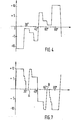
- FIG. 4 shows the "S" curve of the device of FIG. 1, that is to say the characteristic of phase comparator presented by this device.
- Figure 5 shows another distribution of the zones.
- Figure 6 shows another carrier recovery device according to the invention.
- FIG. 7 shows the "S" curve of the device shown in FIG. 6.
- the reference 1 indicates a quadrature detector which supplies signals on wires 1p and 1q from which all the states of a signal d are determined. 'input applied to terminal 2; these signals available on wires 1p and 1q are the projection of the amplitude of the input signal on the components P and 0 in quadrature of a signal supplied by an oscillator 3 provided with a frequency control 4.
- FIG. 2 represents the configuration of these states when the oscillator 3 is considered to be synchronized.
- the modulation of the input signal envisaged is the MAQ16 modulation, that is to say a modulation with 16 states; these states are identified in Figure 2 by E1, E2, E3, ..., E16; the state E1 is characterized by signals of amplitude "1" reported on the components P and Q, the state E3 by signals of amplitude "3” reported on the components P and Q, the state E2 by signals of amplitudes "3" and “1” reported respectively on the components P and Q and the state E4 by signals of amplitudes "1” and "3” reported respectively on the components P and Q.
- the states E5, E6. E7 and E8 occupy symmetrical positions, compared to the component Q in the states E1, E4, E3 and E2.
- means for supplying a correction signal to the frequency control 4 via an integrating low-pass filter 5.
- These means comprise inter alia a circuit for determining zones 10 in the plane P and Q components and according to the invention a weighting circuit 12 at the output of which appears the correction signal dependent, according to variable weights, of different zones defined by the zone determination circuit.
- Different logic circuits will determine different zones from the logic signals provided by these decision circuits.
- Doors “OR EXCLUSIVE" 40, 4 1 and 42 determine zones X represented by the references X1 to X8 in FIG. 3a.
- the door 42 is provided with two inputs, one of which is connected to the output of the door 40 and the other, to the output of the door 41.
- the two inputs of the door 40 are combined at the output of the two decision circuits 19 and 20 and the two inputs of gate 41 at the output of circuits 16 and 18.
- the output signal of gate 42 provides a logic value signal "1" for the hatched areas X2, X4, X6 and X8 and the value "0" for the other zones X1, X3, X5 and X7.
- the "OR" doors 45, 46 and 47 and the "EXCLUSIVE OR” door 48 with inverting output cooperating with the door 42 determine zones Y represented by the references Y1 to Y16 in FIG. 3b.
- the door 48 is provided with a first input which is connected to the outlet of the door 42 and a second one at the outlet of the door 47.
- the door 47 is provided with a first inlet which is connected to the outlet of the door 45 and a second at the exit of door 46; the two inputs of gate 45 are connected respectively to the outputs of decision circuits 30 and 31 and those of gate 46 to the outputs of circuits 32 and 33.
- the output signal of gate 48 provides a signal with logic value "1" for hatched areas Y1, Y4, Y5, Y8, Y9, Y12, Y13 and Y16 and the value "0" for the remaining areas Y2, Y3, Y6, Y7, Y10, Y11, Y14 and Y15.
- the "OR" doors 50, 51 and 52 and the "EXCLUSIVE OR” door 53 cooperating with the door 42 determine zones Z represented by the references Z1 to Z16 in FIG. 3c.
- the door 53 is provided with a first input which is connected to the outlet of the door 42 and a second one at the outlet of the door 52.
- the door 52 is provided with a first inlet which is connected to the outlet of the door 50 and a second at the output of door 51.
- the two inputs of door 50 are respectively connected to the outputs of the circuits decision 34 and 35 and those of gate 51 at the outputs of circuits 36 and 37.
- the output signal of gate 53 provides a logic value signal "1" for the hatched areas Z2, Z3, Z6, Z7, Z10, Z11, Z14 and Z15 and the value "0" for the remaining zones Z1, Z4, Z5, Z8, Z9, Z12, Z13 and Z16.
- the distribution of the zones is determined by successive rotations of the first quadrant around the point of intersection of the lines P and Q.
- the decision circuits can be used to supply logic signals corresponding to the different states E1 to E16. If we call FQ, FP, FQ2; FQ2 ', FP2 and FP2 'the signals at the output of the decision circuits 19, 20, 34, 35, 36 and 37 respectively, a coding circuit 70 supplies signals representing the states E1 to E16.
- the coding circuit 70 performs the following logic operations.
- states can be determined directly by dibits; for example, the first dibit of a state gives the number of the quadrant, this is obtained by the comparators 19 and 20 and the second dibit gives the place of the dibit in the quadrant this is obtained by the comparators 34 to 37 and the doors 50 and 51.
- FIG. 4 the "S" curve, or phase characteristic of the carrier recovery device of FIG. 1, has been represented. On the ordinate, the arbitrary units have been plotted while the abscissa is indicated in degrees . It can be seen that with this device of the invention, we are not confronted with the problems of false clashes.
- the distribution of the zones is deduced by successive rotations of the zones of the first quadrant.
- the device shown in a variant in FIG. 6 realizes the configuration of the zones in FIG. 5.
- This device is formed by a zone determination circuit 10 comprising the elements 15, 16, 17, 18, 19, 20, 34, 35, 36, 37, 40, 41, 42, 50 and 51 already mentioned, a door "OR EXCLUSIVE" 80 whose inputs are connected to the outputs of doors 50 and 51 and whose output is connected to the input of another door "OR EXCLUSIVE" 81, the other input of door 81 is connected to the exit from door 42.
Abstract
Ce dispositif de récupération de la porteuse d'un signal d'entrée modulé par sauts d'amplitude et par sauts de phase (notamment modulation MAQ) est pourvu d'un oscillateur à commande de fréquence (3) pour produire ladite porteuse, d'un détecteur à quadrature (1) pour fournir des signaux représentant l'amplitude du signal d'entrée projetée sur deux composantes P et Q en quadrature du signal fourni par ledit oscillateur et pour déterminer ainsi les états de modulation du signal d'entrée et de moyens de correction pour former, à partir d'un circuit de détermination de zones (10) dans le plan des composantes P et Q, un signal de correction pour ladite commande de fréquence dudit oscillateur. Selon l'invention les moyens de correction comportent un circuit de pondération (12) à la sortie duquel apparaît le signal de correction dépendant selon des poids variables de différentes zones définies par le circuit de détermination de zones. Application: transmission à haut débit binaire.This device for recovering the carrier of an input signal modulated by amplitude jumps and by phase jumps (in particular MAQ modulation) is provided with a frequency control oscillator (3) to produce said carrier, a quadrature detector (1) for supplying signals representing the amplitude of the input signal projected onto two P and Q components in quadrature of the signal supplied by said oscillator and thus for determining the modulation states of the input signal and of correction means for forming, from a circuit for determining zones (10) in the plane of the components P and Q, a correction signal for said frequency control of said oscillator. According to the invention, the correction means comprise a weighting circuit (12) at the output of which the dependent correction signal appears according to variable weights of different zones defined by the zone determination circuit. Application: high bit rate transmission.
Description
L'invention concerne un dispositif de récupération de la porteuse d'un signal d'entrée modulé par sauts d'amplitude et par sauts de phase (notamment modulation MAQ) pourvu d'un oscillateur à commande de fréquence pour produire ladite porteuse, d'un détecteur à quadrature pour fournir des signaux représentant l'amplitude du signal d'entrée projetée sur deux composantes P et Q en quadrature du signal fourni par ledit oscillateur et pour déterminer ainsi les états de modulation du signal d'entrée et de moyens de correction pour former, à partir d'un circuit de détermination de zones dans le plan des composantes P et Q, un signal de correction pour ladite commande de fréquence dudit oscillateur.The invention relates to a device for recovering the carrier of an input signal modulated by amplitude jumps and by phase jumps (in particular MAQ modulation) provided with a frequency-controlled oscillator for producing said carrier, a quadrature detector for supplying signals representing the amplitude of the input signal projected on two components P and Q in quadrature of the signal supplied by said oscillator and for thus determining the states of modulation of the input signal and of correction means to form, from a circuit for determining zones in the plane of the components P and Q, a correction signal for said frequency control of said oscillator.
Un tel dispositif est décrit dans la demande de brevet français n° 2 466 145 déposée le 11 août 1980. Dans ce dispositif connu, le signal de correction est élaboré pour tous les états du signal d'entrée considérés avec la même importance quelle que soit la zone dans laquelle il se trouve. Or si le signal d'entrée est transmis par un canal subissant le phénomème dit "d'évanouissement sélectif", la position des états par rapport aux composantes en quadrature n'est plus celle des points idéaux mais dépend de la succession des états transmis. L'incertitude de ces points est d'autant plus importante que le phénomène d'évanouissement sélectif est prononcé. Il peut même arriver que les domaines d'incertitudes deviennent adjacents. Dans ce cas, le dispositif connu fonctionne mal car les états pour lesquels l'amplitude du signal est faible sont générateurs de bruits et entachent d'erreurs importantes le signal de correction.Such a device is described in French patent application No. 2 466 145 filed on August 11, 1980. In this known device, the correction signal is developed for all the states of the input signal considered with the same importance whatever the area in which it is located. Now if the input signal is transmitted by a channel undergoing the phenomenon known as "selective fading", the position of the states with respect to the quadrature components is no longer that of the ideal points but depends on the succession of the transmitted states. The uncertainty of these points is all the more important as the phenomenon of selective fading is pronounced. It may even happen that the areas of uncertainty become adjacent. In this case, the known device malfunctions because the states for which the amplitude of the signal is low generate noise and taint the correction signal with significant errors.
L'invention propose un dispositif de récupération de porteuse du genre mentionné dans le préambule qui présente un fonctionnement tout aussi satisfaisant tant en présence d'évanouissement sélectif qu'en son absence.The invention proposes a carrier recovery device of the kind mentioned in the preamble which has an equally satisfactory operation both in the presence of selective fading and in its absence.
Pour cela, un tel discositif de récuoération est remar-Pour cela, un tel dispositif de récupération est remarquable en ce que les moyens je correction comportent un circuit de pondération à la sortie duquel apparaît le signal de correction dépendant selon des poids variables de différentes zones définies par le circuit de détermination de zones.For this purpose, such discositif of Regeneration and utilization is remar-for this purpose, such recovery device is characterized in that the j th correcting means comprise a weighting circuit at whose output appears the correction signal dependent according to weight variables in different zones defined by the zone determination circuit.
Un avantage apporté par l'invention est qu'en choisissant convenablement les différents poids du circuit pondéra- tion, il est possible d'éviter le problème de faux accrochages, ce qui peut être décelé par l'examen de la courbe dite courbe en "S" (on se reportera à ce sujet à l'article de A. LECLERT et P. VANDAMME du rapport GLOBECOM'82 intitulé "Universal carrier recovery loop for OASK et PSK signal sets").An advantage provided by the invention is that by properly choosing the different weights of the weighting circuit, it is possible to avoid the problem of false hooks, which can be detected by examining the curve called " S "(see the article by A. LECLERT and P. VANDAMME in the GLOBECOM'82 report entitled" Universal carrier recovery loop for OASK and PSK signal sets ").
La description suivante faite en regard des dessins annexés, le tout donné à titre d'exemple non limitatif, fera bien comprendre comment l'invention peut être réalisée.The following description given with reference to the appended drawings, all given by way of nonlimiting example, will make it clear how the invention can be implemented.
La figure 1 représente un dispositif de récupération de la porteuse d'un signal modulé en modulation MAQ16, dispositif réalisé conformément à l'invention.FIG. 1 represents a device for recovering the carrier of a signal modulated in MAQ16 modulation, device produced in accordance with the invention.
La figure 2 montre la répartition des états de modulation dans le plan P, Q.Figure 2 shows the distribution of modulation states in the P, Q plane.
La figure 3 montre la formation des zones.Figure 3 shows the formation of the zones.
La figure 4 montre la courbe en "S" du dispositif de la figure 1, c'est-à-dire la caractéristique de comparateur de phase que présente ce dispositif.FIG. 4 shows the "S" curve of the device of FIG. 1, that is to say the characteristic of phase comparator presented by this device.
La figure 5 montre une autre répartition des zones.Figure 5 shows another distribution of the zones.
La figure 6 montre un autre dispositif de récupération de porteuse conforme à l'invention.Figure 6 shows another carrier recovery device according to the invention.
La figure 7 montre la courbe en "S" du dispositif montré à la figure 6.FIG. 7 shows the "S" curve of the device shown in FIG. 6.
A la figure 1 où est montré un dispositif de récupération de porteuse conforme à l'invention, la référence 1 indique un détecteur à quadrature qui fournit des signaux sur des fils 1p et 1q à partir desquels on détermine tous les états d'un signal d'entrée appliqué à la borne 2; ces signaux disponibles sur des fils 1p et 1q sont la projection de l'amplitude du signal d'entrée sur les composants P et 0 en quadrature d'un signal fourni par un oscillateur 3 muni d'une commande de fréquence 4. La figure 2 représente la configuration de ces états lorsque l'oscillateur 3 est considéré comme synchronisé. Dans cet exemple décrit la modulation du signal d'entrée envisagée est la modulation MAQ16 c'est-à-dire une modulation à 16 états; ces états sont repérés sur la figure 2 par El, E2, E3, ..., E16; l'état E1 est caractérisé par des signaux d'amplitude "1" rapportée sur les composantes P et Q, l'état E3 par des signaux d'amplitude "3" rapportée sur les composantes P et Q, l'état E2 par des signaux d'amplitudes "3" et "1" rapportées respectivement sur les composantes P et Q et l'état E4 par des signaux d'amplitudes "1" et "3" rapportées respectivement sur les composantes P et Q. Les états E5, E6. E7 et E8 occupent des positions symétriques, par rapport à la composante Q aux états E1, E4, E3 et E2. Quant aux états E9, E10,E11, E12, E13, E14, E15 et E16 ils occupent des positions symétriques, par rapport à la composante P, aux états E5, E8, E7, E6, E1, E4, E3 et E2 respectivement.In FIG. 1 where a carrier recovery device according to the invention is shown, the
Si, notamment, l'oscillateur n'est pas synchronisé avec le signal d'entrée, les états n'occupent plus les positions idéales définies ci-dessus. Pour ramener ces états vers leurs positions initiales, on a prévu des moyens pour fournir un signal de correction à la commande de fréquence 4 via un filtre passe-bas intégrateur 5. Ces moyens comportent entre autres un circuit de détermination de zones 10 dans le plan des composantes P et Q et conformément à l'invention un circuit de pondération 12 à la sortie duquel apparaît le signal de correction dépendant, selon des poids variables, de différentes zones définies par le circuit de détermination de zones.If, in particular, the oscillator is not synchronized with the input signal, the states no longer occupy the ideal positions defined above. To bring these states back to their initial positions, means have been provided for supplying a correction signal to the
Le circuit de détermination de zones 10 comprend un additionneur 15 dont les entrées sont connectées aux fils 1p et 1q et dont la sortie est connectée à un circuit de décision 16, un organe de soustraction 17 dont l'entrée (+) est connectée au fil 1q, dont l'entrée (-) est connectée au fil 1p et dont la sortie est connectée à un circuit de décision 18, un circuit de décision 19 dont l'entrée est connectée au fil 1q et un circuit de décision 20 dont l'entrée est connectée au fil 1p. Les circuits 16, 18, 19 et 20 fournissent un signal logique de valeur "1" lorsque le signal à leur entrée est supérieur à "0" et la valeur logique "0" si le signal ne l'est pas. Les valeurs logiques à la sortie apparaissent à la cadence d'apparition des différents états du signal d'état. Pour cela il est prévu, comme cela est connu, un générateur de cadencement 25 qui fournit des signaux H représentant cette cadence d'apparition et ces signaux H sont appliqués aux différents circuits de décision 16, 18, 19 et 20. D'autres circuits de décision sont prévus :
- - le
circuit 30 dont l'entrée est connectée au fil 1q fournit un signal "1" pour un signal d'entrée supérieur à "+3" et "0" autrement - - le circuit 31 dont l'entrée est connectée au fil 1q fournit un signal "1" pour un signal d'entrée inférieur à "-3" et "0" autrement
- - le
circuit 32 dont l'entrée est connectée au fil 1p fournit un signal "1" pour un signal d'entrée supérieur à "+3" et "0" autrement - - le
circuit 33 dont l'entrée est connectée au fil 1p fournit un signal "1" pour un signal d'entrée inférieur à "-3" et "0" autrement - - le
circuit 34 dont l'entrée est connectée au fil 1q fournit un signal "1" pour un signal d'entrée supérieur à "+2" et "0" autrement - - le
circuit 35 dont l'entrée est connectée au fil 1q fournit un signal "1" pour un signal d'entrée inférieur à "-2" et "0" autrement - - le
circuit 36 dont l'entrée est connectée au fil 1p fournit un signal ''1'' pour un signal d'entrée supérieur à "+2" et "0" autrement - - le
circuit 37 dont l'entrée est connectée au fil 1p fournit un signal "1" pour un signal d'entrée inférieur à "-2'' et "0" autrement.
- -
circuit 30, the input of which is connected to wire 1q, provides a signal "1" for an input signal greater than "+3" and "0" otherwise - - circuit 31 whose input is connected to wire 1q provides a signal "1" for an input signal less than "-3" and "0" otherwise
- -
circuit 32 whose input is connected to wire 1p provides a signal "1" for an input signal greater than "+3" and "0" otherwise - -
circuit 33 whose input is connected to wire 1p provides a signal "1" for an input signal less than "-3" and "0" otherwise - -
circuit 34 whose input is connected to wire 1q provides a signal "1" for an input signal greater than "+2" and "0" otherwise - -
circuit 35 whose input is connected to wire 1q provides a signal "1" for an input signal less than "-2" and "0" otherwise - -
circuit 36 whose input is connected to wire 1p provides a signal "1" for an input signal greater than "+2" and "0" otherwise - - The
circuit 37 whose input is connected to the wire 1p provides a signal "1" for an input signal less than "-2" and "0" otherwise.
Différents circuits logiques vont déterminer différentes zones à partir des signaux logiques fournis par ces circuits de décision.Different logic circuits will determine different zones from the logic signals provided by these decision circuits.
Les portes "OU EXCLUSIF" 40, 41 et 42 déterminent des zones X représentées par les références X1 à X8 a la figure 3a. La porte 42 est munie de deux entrées dont une est connectée à la sortie de la porte 40 et l'autre, a la sortie de la porte 41. Les deux entrées de la porte 40 sont réunies à la sortie des deux circuits de décision 19 et 20 et les deux entrées de la porte 41 à la sortie des circuits 16 et 18. Le signal de sortie de la porte 42 fournit un signal de valeur logique "1" pour les zones hachurées X2, X4, X6 et X8 et la valeur "0" pour les autres zones X1, X3, X5 et X7. Ces différentes zones sont délimitées d'une part par les axes P et Q et d'autre part par les droites d'équation p+q=0 et p-q=0 où p est la valeur d'abscisse et q la valeur d'ordonnée.Doors "OR EXCLUSIVE" 40, 4 1 and 42 determine zones X represented by the references X1 to X8 in FIG. 3a. The
Les portes "OU" 45, 46 et 47 et la porte "OU EXCLUSIF" 48 à sortie inverseuse coopérant avec la porte 42 déterminent des zones Y représentées par les références Y1 à Y16 à la figure 3b. La porte 48 est munie d'une première entrée qui est connectée à la sortie de la porte 42 et une deuxième à la sortie de la porte 47. La porte 47 est munie d'une première entrée qui est connectée à la sortie de la porte 45 et d'une deuxième à la sortie de la porte 46; les deux entrées de la porte 45 sont reliées respectivement aux sorties des circuits de décision 30 et 31 et celles de la porte 46 aux sorties des circuits 32 et 33. Le signal de sortie de la porte 48 fournit un signal de valeur logique "1" pour les zones hachurées Y1, Y4, Y5, Y8, Y9, Y12, Y13 et Y16 et la valeur "0" pour les zones restantes Y2, Y3, Y6, Y7, Y10, Y11, Y14 et Y15. Dans le plan P, Q ces zones sont délimitées d'une part par les axes P, Q et les droites p + q = 0 et p - q = 0 et d'autre part par un carré défini par les droites p = 3, P = -3, q = 3 et q =-3.The "OR"
Les portes "OU" 50, 51 et 52 et la porte "OU EXCLUSIF" 53 coopérant avec la porte 42 déterminent des zones Z représentées par les références Z1 à Z16 à la figure 3c. La porte 53 est munie d'une première entrée qui est connectée à la sortie de la porte 42 et une deuxième à la sortie de la porte 52. La porte 52 est munie d'une première entrée qui est connectée à la sortie de la porte 50 et d'une deuxième à la sortie de la porte 51. Les deux entrées de la porte 50 sont reliées respectivement aux sorties des circuits de décision 34 et 35 et celles de la porte 51 aux sorties des circuits 36 et 37. Le signal de sortie de la porte 53 fournit un signal de valeur logique "1" pour les zones hachurées Z2, Z3, Z6, Z7, Z10, Z11, Z14 et Z15 et la valeur "0" pour les zones restantes Z1, Z4, Z5, Z8, Z9, Z12, Z13 et Z16. Dans le plan P, Q ces zones sont délimitées d'une part par les axes P, Q et les droites p + q = 0, p - q = 0 et d'autre part par un carré défini par les droites p = 2, p = -2, q = 2 et q = -2.The "OR"
A partir des signaux de sortie des portes 42, 48 et 53 le circuit de pondération fournit un signal au filtre passe-bas intégrateur de la manière suivante :
- - aux valeurs logiques "1" des signaux de sortie des portes 42, 48
et 53 on affecte respectivement des valeurs positives +x, +y, +z et aux valeurs "0", -x, -y, -z. - - ces valeurs affectées sont ensuite additionnées
par un additionneur 60.
- - to the logical values "1" of the output signals of the
gates - - these assigned values are then added by an
adder 60.
Si les valeurs de x, y, z sont telles que x=3,5, y=2 et z=0,5 on définit alors des zones de pondération ZP1, ZP2, ZP3, ZP4, ZP5 et ZP6 représentées à la figure 3d qui ne montre que le premier quadrant du plan P, Q.If the values of x, y, z are such that x = 3.5, y = 2 and z = 0.5 we then define weighting zones ZP1, ZP2, ZP3, ZP4, ZP5 and ZP6 shown in Figure 3d which shows only the first quadrant of the plane P, Q.
A la zone ZP1 délimitée par l'axe P, la droite p - q = 0 et la droite p = 2, la valeur "-2" est affectée.In the zone ZP1 delimited by the axis P, the line p - q = 0 and the line p = 2, the value "-2" is assigned.
A la zone ZP2 délimitée par l'axe P, la droite p - q = 0 et la droite p = 2 et la droite p = 3, la valeur "-1" est affectée.In the zone ZP2 delimited by the axis P, the line p - q = 0 and the line p = 2 and the line p = 3, the value "-1" is assigned.
A la zone ZP3 délimitée par l'axe P, la droite p - q = 0 et la droite p = 3, la valeur "-5" est affectée.In the zone ZP3 delimited by the axis P, the line p - q = 0 and the line p = 3, the value "-5" is assigned.
Aux zones ZP4, ZP5 et ZP6 symétriques, par rapport à la droite p - q = 0, aux zones ZP1, ZP2 et ZP3 les valeurs "+2", "+1" et "+5" sont respectivement affectées.In zones ZP4, ZP5 and ZP6 symmetrical, with respect to the line p - q = 0, in zones ZP1, ZP2 and ZP3 the values "+2", "+1" and "+5" are respectively assigned.
Pour les autres quadrants, la répartition des zones se détermine par des rotations successives du premier quadrant autour du point d'intersection des droites P et Q.For the other quadrants, the distribution of the zones is determined by successive rotations of the first quadrant around the point of intersection of the lines P and Q.
Il est intéressant de noter que les circuits de décision peuvent être utilisés pour fournir des signaux logiques correspondant aux différents états El à E16. Si on apelle FQ, FP, FQ2; FQ2', FP2 et FP2' les signaux à la sortie des circuits de décision 19, 20, 34, 35, 36 et 37 respectivement, un circuit de codage 70 fournit des signaux représentant les états E1 à E16. Le circuit de codage 70 effectue les opérations logiques suivantes.
Il est bien évident qu'à partir des circuits de décision et des circuits logiques, les états peuvent être déterminés directement par des dibits; par exemple, le premier dibit d'un état donne le numéro du quadrant, ceci est obtenu par les comparateurs 19 et 20 et le deuxième dibit donne la place du dibit dans le quadrant ceci est obtenu par les comparateurs 34 à 37 et les portes 50 et 51.It is obvious that from decision circuits and logic circuits, states can be determined directly by dibits; for example, the first dibit of a state gives the number of the quadrant, this is obtained by the
On a représenté à la figure 4, la courbe en "S", ou caractéristique de phase du dispositif de récupération de porteuse de la figure 1. En ordonnées, on a porté les unités arbitraires tandis qu'en abscisses les angles sont repérés en degrés. On constate qu'avec ce dispositif de l'invention, on n'est pas confronté avec les problèmes de faux accrochages.In FIG. 4, the "S" curve, or phase characteristic of the carrier recovery device of FIG. 1, has been represented. On the ordinate, the arbitrary units have been plotted while the abscissa is indicated in degrees . It can be seen that with this device of the invention, we are not confronted with the problems of false clashes.
Au lieu des zones montrées à la figure 3d on peut prendre la configuration de zones ZP100 à ZP105 indiquées à la figure 5.Instead of the zones shown in figure 3d we can take the configuration of zones ZP100 to ZP105 indicated in figure 5.
A la zone ZP100 délimitée par l'axe P, la droite p - q = 0 et la droite p = 2 la valeur "-5" est affectée.In the zone ZP100 delimited by the axis P, the straight line p - q = 0 and the line p = 2 the value "-5" is assigned.
A la zone ZP101 délimitée par l'axe P, la droite q = 2 et la droite p = 2 la valeur "-1" est affectée.In the zone ZP101 delimited by the axis P, the line q = 2 and the line p = 2 the value "-1" is assigned.
A la zone ZP102 délimitée par la droite p - q = 0 et la droite q = 2 la valeur "-5" est affectée.To the zone ZP102 delimited by the line p - q = 0 and the line q = 2 the value "-5" is assigned.
Aux zones ZP103, ZP104 et ZP105 symétriques, par rapport à la droite p - q = 0, aux zones ZP102, ZP101 et ZP100 sont affectées respectivement les valeurs "+5", "+1" et "+5".In zones ZP103, ZP104 and ZP105 symmetrical, with respect to the line p - q = 0, in zones ZP102, ZP101 and ZP100 are assigned the values "+5", "+1" and "+5" respectively.
Pour les autres quadrants, la répartition des zones se déduit par des rotations successives des zones du premier quadrant.For the other quadrants, the distribution of the zones is deduced by successive rotations of the zones of the first quadrant.
Le dispositif montré en variante à la figure 6 réalise la configuration de zones de la figure 5. Les éléments communs avec ceux de la figure 1 portent les mêmes références. Ce dispositif est formé d'un circuit de détermination de zones 10 comportant les éléments 15, 16, 17, 18, 19, 20, 34, 35, 36, 37, 40, 41, 42, 50 et 51 déjà cités, une porte "OU EXCLUSIF" 80 dont les entrées sont reliées aux sorties des portes 50 et 51 et dont la sortie est reliée à l'entrée d'une autre porte "OU EXCLUSIF" 81, l'autre entrée de la porte 81 est reliée à la sortie de la porte 42. A la sortie de la porte 42 on a un signal qui détermine les zones X déjà citées et à la sortie de la porte 81 on a un signal qui détermine des zones V et qui, combiné avec celui des X au moyen du circuit de pondération 12, permet d'obtenir la configuration de zones montrée à la figure 5. Pour cela, le circuit de pondération affecte la valeur v = 2 pour un signal de valeur logique "1" à la sortie de la porte 81 et la valeur v = -2 pour la valeur logique "0" et affecte la valeur x = 3 pour un signal de valeur logique "1" à la sortie de la porte 42 et la valeur x = -3 pour un signal de valeur logique "0".The device shown in a variant in FIG. 6 realizes the configuration of the zones in FIG. 5. The elements common with those of FIG. 1 have the same references. This device is formed by a
Cependant la courbe "S" présente deux plages A et B où l'on peut théoriquement avoir des phénomènes de faux accrochages. En pratique, comme ces points sont situés sur l'axe des abscisses ces phénomènes ne se produisent pas.However the curve "S" presents two ranges A and B where one can theoretically have phenomena of false hookings. In practice, as these points are located on the abscissa axis these phenomena do not occur.
Claims (4)
Applications Claiming Priority (2)
| Application Number | Priority Date | Filing Date | Title |
|---|---|---|---|
| FR8303688 | 1983-03-07 | ||
| FR8303688A FR2542536B1 (en) | 1983-03-07 | 1983-03-07 | DEVICE FOR RECOVERING THE CARRIER OF AN INPUT SIGNAL MODULATED BY AMPLITUDE HOP AND PHASE HOP |
Publications (2)
| Publication Number | Publication Date |
|---|---|
| EP0118156A1 true EP0118156A1 (en) | 1984-09-12 |
| EP0118156B1 EP0118156B1 (en) | 1986-10-15 |
Family
ID=9286560
Family Applications (1)
| Application Number | Title | Priority Date | Filing Date |
|---|---|---|---|
| EP84200288A Expired EP0118156B1 (en) | 1983-03-07 | 1984-03-01 | Circuit recovering the carrier of a signal modulated by amplitude steps and phase steps |
Country Status (9)
| Country | Link |
|---|---|
| US (1) | US4587498A (en) |
| EP (1) | EP0118156B1 (en) |
| JP (1) | JPS59168750A (en) |
| AU (1) | AU558495B2 (en) |
| CA (1) | CA1208712A (en) |
| DE (1) | DE3461013D1 (en) |
| FI (1) | FI82165C (en) |
| FR (1) | FR2542536B1 (en) |
| NO (1) | NO840819L (en) |
Cited By (7)
| Publication number | Priority date | Publication date | Assignee | Title |
|---|---|---|---|---|
| WO1986000940A1 (en) * | 1984-07-20 | 1986-02-13 | Hughes Aircraft Company | Growth of single crystal cadmium-indium-telluride |
| FR2581277A1 (en) * | 1985-04-30 | 1986-10-31 | Labo Electronique Physique | VEHICLE WAVE RECOVERY CIRCUIT FOR DIGITAL TRANSMISSION SYSTEMS |
| EP0224556A1 (en) * | 1985-05-20 | 1987-06-10 | Telebit Corp | Ensemble modem structure for imperfect transmission media. |
| EP0692896A1 (en) * | 1994-07-12 | 1996-01-17 | Laboratoires D'electronique Philips S.A.S. | QAM carrier recovery |
| FR2722630A1 (en) * | 1994-07-12 | 1996-01-19 | Philips Electronique Lab | Carrier recovery system for digital signal transmissions |
| FR2733107A1 (en) * | 1995-04-12 | 1996-10-18 | Philips Electronique Lab | Digital transmission system e.g. for optical communication |
| EP1940104A3 (en) * | 2006-12-29 | 2012-07-25 | Trident Microsystems (Far East) Ltd. | Method and device for determining a symbol when receiving a signal coupled with a quadrature signal pair for QAM frequency control and/or rotation control |
Families Citing this family (16)
| Publication number | Priority date | Publication date | Assignee | Title |
|---|---|---|---|---|
| US4991030A (en) * | 1986-07-07 | 1991-02-05 | Canon Kabushiki Kaisha | Image reading apparatus capable of reading a projected image and having means for diffusing the projected luminous flux |
| US4686689A (en) * | 1986-07-24 | 1987-08-11 | Graham-Patten Systems, Inc. | Phase-locked loop circuit |
| US4712221A (en) * | 1986-08-29 | 1987-12-08 | International Business Machines Corporation | Carrier recovery of modulated signals |
| DE58907579D1 (en) * | 1989-01-18 | 1994-06-01 | Siemens Ag | Digital distortion. |
| GB2323505B (en) * | 1994-03-18 | 1998-11-04 | Fujitsu Ltd | Radio receiver for use in the reception of digital multiplexing signals |
| JP2911773B2 (en) * | 1994-03-18 | 1999-06-23 | 富士通株式会社 | Digital multiplex radio receiver |
| US5519733A (en) * | 1994-05-05 | 1996-05-21 | General Instrument Corporation Of Delaware | Method and apparatus for recovering a qam carrier |
| US5987069A (en) * | 1996-12-24 | 1999-11-16 | Gte Government Systems Corporation | Method and apparatus for variably allocating upstream and downstream communication spectra |
| CA2274718A1 (en) * | 1996-12-24 | 1998-07-02 | Gte Government Systems Corporation | Symbol lock detector |
| US6304594B1 (en) | 1998-07-27 | 2001-10-16 | General Dynamics Government Systems Corporation | Interference detection and avoidance technique |
| US6560294B1 (en) | 1998-09-25 | 2003-05-06 | Texas Instruments Incorporated | Phase estimation in carrier recovery of phase-modulated signals such as QAM signals |
| US6212229B1 (en) | 1998-12-16 | 2001-04-03 | General Dynamics Government Systems Corporation | Adaptive pre-emphasis technique |
| US6707863B1 (en) | 1999-05-04 | 2004-03-16 | Northrop Grumman Corporation | Baseband signal carrier recovery of a suppressed carrier modulation signal |
| US8000667B2 (en) * | 2006-02-03 | 2011-08-16 | Johnson Controls Technology Company | System and method for compensating for modulation induced frequency shift during transmission of a radio frequency signal |
| US8259859B2 (en) * | 2009-09-21 | 2012-09-04 | Techwell Llc | Method and system for carrier recovery for QAM |
| JP6156807B2 (en) * | 2013-11-15 | 2017-07-05 | 国立研究開発法人産業技術総合研究所 | Received signal processing apparatus, communication system, and received signal processing method |
Citations (3)
| Publication number | Priority date | Publication date | Assignee | Title |
|---|---|---|---|---|
| US3970946A (en) * | 1973-07-12 | 1976-07-20 | Nippon Electric Company, Ltd. | Demodulator for amplitude-and-phase modulated signals having control means for reducing phase and amplitude errors |
| US4057762A (en) * | 1975-12-26 | 1977-11-08 | Nippon Electric Company, Ltd. | Device for phase synchronizing a reproduced reference carrier signal with windows specified for preselected ones of amplitude and phase modulated signal points |
| DE3030145A1 (en) * | 1979-08-10 | 1981-02-26 | Nippon Electric Co | PHASE SYNCHRONIZATION CIRCUIT FOR TRANSMITTING SIGNALS WITH MULTI-STAGE, MULTI-PHASE OVERLAY MODULATION |
-
1983
- 1983-03-07 FR FR8303688A patent/FR2542536B1/en not_active Expired
-
1984
- 1984-03-01 EP EP84200288A patent/EP0118156B1/en not_active Expired
- 1984-03-01 DE DE8484200288T patent/DE3461013D1/en not_active Expired
- 1984-03-01 CA CA000448668A patent/CA1208712A/en not_active Expired
- 1984-03-02 FI FI840842A patent/FI82165C/en not_active IP Right Cessation
- 1984-03-05 NO NO840819A patent/NO840819L/en unknown
- 1984-03-06 AU AU25301/84A patent/AU558495B2/en not_active Ceased
- 1984-03-07 JP JP59042230A patent/JPS59168750A/en active Granted
- 1984-03-07 US US06/587,089 patent/US4587498A/en not_active Expired - Fee Related
Patent Citations (3)
| Publication number | Priority date | Publication date | Assignee | Title |
|---|---|---|---|---|
| US3970946A (en) * | 1973-07-12 | 1976-07-20 | Nippon Electric Company, Ltd. | Demodulator for amplitude-and-phase modulated signals having control means for reducing phase and amplitude errors |
| US4057762A (en) * | 1975-12-26 | 1977-11-08 | Nippon Electric Company, Ltd. | Device for phase synchronizing a reproduced reference carrier signal with windows specified for preselected ones of amplitude and phase modulated signal points |
| DE3030145A1 (en) * | 1979-08-10 | 1981-02-26 | Nippon Electric Co | PHASE SYNCHRONIZATION CIRCUIT FOR TRANSMITTING SIGNALS WITH MULTI-STAGE, MULTI-PHASE OVERLAY MODULATION |
Cited By (11)
| Publication number | Priority date | Publication date | Assignee | Title |
|---|---|---|---|---|
| WO1986000940A1 (en) * | 1984-07-20 | 1986-02-13 | Hughes Aircraft Company | Growth of single crystal cadmium-indium-telluride |
| EP0187843A1 (en) * | 1984-07-20 | 1986-07-23 | Hughes Aircraft Co | Growth of single crystal cadmium-indium-telluride. |
| FR2581277A1 (en) * | 1985-04-30 | 1986-10-31 | Labo Electronique Physique | VEHICLE WAVE RECOVERY CIRCUIT FOR DIGITAL TRANSMISSION SYSTEMS |
| EP0200271A1 (en) * | 1985-04-30 | 1986-11-05 | Laboratoires D'electronique Philips | Carrier recovery circuit for digital transmission systems |
| EP0224556A1 (en) * | 1985-05-20 | 1987-06-10 | Telebit Corp | Ensemble modem structure for imperfect transmission media. |
| EP0224556A4 (en) * | 1985-05-20 | 1989-10-24 | Telebit Corp | Ensemble modem structure for imperfect transmission media. |
| EP0692896A1 (en) * | 1994-07-12 | 1996-01-17 | Laboratoires D'electronique Philips S.A.S. | QAM carrier recovery |
| FR2722630A1 (en) * | 1994-07-12 | 1996-01-19 | Philips Electronique Lab | Carrier recovery system for digital signal transmissions |
| US5684842A (en) * | 1994-07-12 | 1997-11-04 | U.S. Philips Corporation | Digital transmission system comprising a receiver which includes a carrier recovery circuit |
| FR2733107A1 (en) * | 1995-04-12 | 1996-10-18 | Philips Electronique Lab | Digital transmission system e.g. for optical communication |
| EP1940104A3 (en) * | 2006-12-29 | 2012-07-25 | Trident Microsystems (Far East) Ltd. | Method and device for determining a symbol when receiving a signal coupled with a quadrature signal pair for QAM frequency control and/or rotation control |
Also Published As
| Publication number | Publication date |
|---|---|
| US4587498A (en) | 1986-05-06 |
| DE3461013D1 (en) | 1986-11-20 |
| EP0118156B1 (en) | 1986-10-15 |
| JPS59168750A (en) | 1984-09-22 |
| FI82165B (en) | 1990-09-28 |
| FI840842A (en) | 1984-09-08 |
| NO840819L (en) | 1984-09-10 |
| FI82165C (en) | 1991-01-10 |
| CA1208712A (en) | 1986-07-29 |
| AU2530184A (en) | 1984-09-13 |
| FR2542536B1 (en) | 1985-07-12 |
| JPH0422380B2 (en) | 1992-04-16 |
| FR2542536A1 (en) | 1984-09-14 |
| FI840842A0 (en) | 1984-03-02 |
| AU558495B2 (en) | 1987-01-29 |
Similar Documents
| Publication | Publication Date | Title |
|---|---|---|
| EP0118156B1 (en) | Circuit recovering the carrier of a signal modulated by amplitude steps and phase steps | |
| EP0125723B1 (en) | Carrier frequency equalizing apparatus controlled by base-band signals | |
| EP0054829B1 (en) | Method and apparatus for detecting the training sequence of an autoadaptive equalizer | |
| FR2673344A1 (en) | PHASE / FREQUENCY COMPARATOR FOR RHYTHM RECOVERY CIRCUIT. | |
| DE69730990T2 (en) | DEVICE AND METHOD FOR THE SEQUENTIAL EVALUATION OF COMMUNICATION SIGNALS TO THE MAXIMUM PROBABILITY THROUGH THE USE OF WHITE NOISE PATHING METHODS | |
| JPS5820181B2 (en) | Tasoui Soudou Kifukuchiyousouchi | |
| EP0599722B1 (en) | Apparatus for band clock recovery in a modem receiver | |
| EP0630137A1 (en) | System for the reception of a phase and amplitude modulated digital signal | |
| EP0579100B1 (en) | Method and apparatus for baseband phase correction in a PSK receiver | |
| FR2466145A1 (en) | PHASE SYNCHRONIZATION CIRCUIT FOR MULTI-PHASE, MULTI-LEVEL OVERLAY MODULATED SIGNAL TRANSMISSION SYSTEM | |
| US3727134A (en) | Auto equalizer apparatus | |
| FR2773925A1 (en) | Phase lock loop locking condition detection | |
| CA1052451A (en) | Demodulator for differential phase modulated trains_ | |
| FR2689712A1 (en) | Device for demodulating digital signals modulated according to a technique with alternating modulation constellations. | |
| FR2505111A1 (en) | CARRIER RECOVERY DEVICE FOR 16-STATE AMPLITUDE AND PHASE MODULATION AND DIGITAL DATA RECEIVING SYSTEM COMPRISING SUCH A DEVICE | |
| Osborne | A Generalized" Polarity-Type" Costas Loop for Tracking MPSK Signals | |
| EP1179936B1 (en) | Demodulator for CPFSK signals using a linear approximation of the CPFSK signal | |
| JP3294017B2 (en) | Digital generation method of complex baseband signal | |
| CN106330338B (en) | A kind of signal phase regeneration method and device | |
| DE10300267B4 (en) | Demodulating a frequency modulated received signal by mapping the zero crossings to a sequence of parameter values | |
| Wulich et al. | Synthesis of discrete time-varying null filters for frequency-varying signals using the time-warping technique | |
| DE69909516T2 (en) | METHOD FOR RECEIVING SPREADING SPECTRUM SIGNALS WITH CORRECTION OF THE FREQUENCY OFFICE | |
| US20040223567A1 (en) | Clock recovery system | |
| Goodwin et al. | Choice of basis functions for continuous and discrete system modelling | |
| JP3905195B2 (en) | Method and apparatus for detecting error on frequency of carrier wave |
Legal Events
| Date | Code | Title | Description |
|---|---|---|---|
| PUAI | Public reference made under article 153(3) epc to a published international application that has entered the european phase |
Free format text: ORIGINAL CODE: 0009012 |
|
| AK | Designated contracting states |
Designated state(s): BE CH DE FR GB IT LI NL SE |
|
| 17P | Request for examination filed |
Effective date: 19841130 |
|
| GRAA | (expected) grant |
Free format text: ORIGINAL CODE: 0009210 |
|
| AK | Designated contracting states |
Kind code of ref document: B1 Designated state(s): BE CH DE FR GB IT LI NL SE |
|
| REF | Corresponds to: |
Ref document number: 3461013 Country of ref document: DE Date of ref document: 19861120 |
|
| ITF | It: translation for a ep patent filed |
Owner name: ING. C. GREGORJ S.P.A. |
|
| PGFP | Annual fee paid to national office [announced via postgrant information from national office to epo] |
Ref country code: NL Payment date: 19870331 Year of fee payment: 4 |
|
| PLBE | No opposition filed within time limit |
Free format text: ORIGINAL CODE: 0009261 |
|
| STAA | Information on the status of an ep patent application or granted ep patent |
Free format text: STATUS: NO OPPOSITION FILED WITHIN TIME LIMIT |
|
| 26N | No opposition filed | ||
| PG25 | Lapsed in a contracting state [announced via postgrant information from national office to epo] |
Ref country code: LI Effective date: 19890331 Ref country code: CH Effective date: 19890331 |
|
| PG25 | Lapsed in a contracting state [announced via postgrant information from national office to epo] |
Ref country code: NL Effective date: 19891001 |
|
| NLV4 | Nl: lapsed or anulled due to non-payment of the annual fee | ||
| REG | Reference to a national code |
Ref country code: CH Ref legal event code: PL |
|
| REG | Reference to a national code |
Ref country code: FR Ref legal event code: TP |
|
| ITTA | It: last paid annual fee | ||
| ITPR | It: changes in ownership of a european patent |
Owner name: CESSIONE;TRT TELECOMMUNICATIONS RADIOELECTRIQUES E |
|
| REG | Reference to a national code |
Ref country code: GB Ref legal event code: 732E |
|
| EAL | Se: european patent in force in sweden |
Ref document number: 84200288.3 |
|
| PGFP | Annual fee paid to national office [announced via postgrant information from national office to epo] |
Ref country code: BE Payment date: 19960228 Year of fee payment: 13 |
|
| PGFP | Annual fee paid to national office [announced via postgrant information from national office to epo] |
Ref country code: GB Payment date: 19960229 Year of fee payment: 13 |
|
| PGFP | Annual fee paid to national office [announced via postgrant information from national office to epo] |
Ref country code: SE Payment date: 19960326 Year of fee payment: 13 |
|
| PGFP | Annual fee paid to national office [announced via postgrant information from national office to epo] |
Ref country code: FR Payment date: 19960327 Year of fee payment: 13 |
|
| REG | Reference to a national code |
Ref country code: FR Ref legal event code: TP |
|
| PGFP | Annual fee paid to national office [announced via postgrant information from national office to epo] |
Ref country code: DE Payment date: 19960523 Year of fee payment: 13 |
|
| REG | Reference to a national code |
Ref country code: GB Ref legal event code: 732E |
|
| PG25 | Lapsed in a contracting state [announced via postgrant information from national office to epo] |
Ref country code: GB Effective date: 19970301 |
|
| PG25 | Lapsed in a contracting state [announced via postgrant information from national office to epo] |
Ref country code: SE Effective date: 19970302 |
|
| PG25 | Lapsed in a contracting state [announced via postgrant information from national office to epo] |
Ref country code: BE Effective date: 19970331 |
|
| BERE | Be: lapsed |
Owner name: PHILIPS COMMUNICATION D'ENTREPRISE Effective date: 19970331 |
|
| GBPC | Gb: european patent ceased through non-payment of renewal fee |
Effective date: 19970301 |
|
| PG25 | Lapsed in a contracting state [announced via postgrant information from national office to epo] |
Ref country code: FR Free format text: LAPSE BECAUSE OF NON-PAYMENT OF DUE FEES Effective date: 19971128 |
|
| PG25 | Lapsed in a contracting state [announced via postgrant information from national office to epo] |
Ref country code: DE Effective date: 19971202 |
|
| EUG | Se: european patent has lapsed |
Ref document number: 84200288.3 |
|
| REG | Reference to a national code |
Ref country code: FR Ref legal event code: ST |