EP0116287A2 - Dynamic re-programmable PLA - Google Patents
Dynamic re-programmable PLA Download PDFInfo
- Publication number
- EP0116287A2 EP0116287A2 EP84100235A EP84100235A EP0116287A2 EP 0116287 A2 EP0116287 A2 EP 0116287A2 EP 84100235 A EP84100235 A EP 84100235A EP 84100235 A EP84100235 A EP 84100235A EP 0116287 A2 EP0116287 A2 EP 0116287A2
- Authority
- EP
- European Patent Office
- Prior art keywords
- coupled
- array
- output
- lines
- transistor means
- Prior art date
- Legal status (The legal status is an assumption and is not a legal conclusion. Google has not performed a legal analysis and makes no representation as to the accuracy of the status listed.)
- Withdrawn
Links
Images


Classifications
-
- H—ELECTRICITY
- H03—ELECTRONIC CIRCUITRY
- H03K—PULSE TECHNIQUE
- H03K19/00—Logic circuits, i.e. having at least two inputs acting on one output; Inverting circuits
- H03K19/02—Logic circuits, i.e. having at least two inputs acting on one output; Inverting circuits using specified components
- H03K19/173—Logic circuits, i.e. having at least two inputs acting on one output; Inverting circuits using specified components using elementary logic circuits as components
- H03K19/177—Logic circuits, i.e. having at least two inputs acting on one output; Inverting circuits using specified components using elementary logic circuits as components arranged in matrix form
- H03K19/17704—Logic circuits, i.e. having at least two inputs acting on one output; Inverting circuits using specified components using elementary logic circuits as components arranged in matrix form the logic functions being realised by the interconnection of rows and columns
- H03K19/17708—Logic circuits, i.e. having at least two inputs acting on one output; Inverting circuits using specified components using elementary logic circuits as components arranged in matrix form the logic functions being realised by the interconnection of rows and columns using an AND matrix followed by an OR matrix, i.e. programmable logic arrays
- H03K19/17712—Logic circuits, i.e. having at least two inputs acting on one output; Inverting circuits using specified components using elementary logic circuits as components arranged in matrix form the logic functions being realised by the interconnection of rows and columns using an AND matrix followed by an OR matrix, i.e. programmable logic arrays one of the matrices at least being reprogrammable
Definitions
- This invention relates to programmable logic arrays (PLA's), and more particularly, to PLA's which are readily re-programnable.
- a PLA is a logic circuit which receives a plurality of digital input signals and generates a plurality of digital output signals wherein each of the digital output signals is a programmable sum-of-product combination of the input signals.
- one circuit is provided for generating a plurality of terms which are the logical AND of selected input signals; and another circuit is provided to generate the output signals by selectively ORing the AND terms.
- a typical PLA may have a total of n input signals, generate a total of m AND terms from the input signals, and generate a total of k output signals by selectively ORing the m AND terms.
- the general design of a PLA includes an AND array feeding into an OR array.
- the AND array accepts n address inputs which includes an array of terms m deep. Each term is the AND combination of data, or data complement or don't care for each input (don't care is formed by ignoring data and data complement for a given input), hence a typical program may appear as:
- each.term line may be selectively OR'd into an output (the array is m X k where k is the number of outputs).
- PLA's are typically designed for use in systems requiring permanent or semipermanent nonvolatile logic arrays.
- PROM's programmable read only memories
- EPROM's erasable PROM's
- EPROM's can be changed by the use of an ultraviolet light, which erasure requires several hours to complete.
- another problem with EPROM's is that they are expensive.
- EEPROM's electrically erasable PROM's
- EPROM's require special power supplies.
- PROM's are not configured as PLA's.
- An advantage of the present invention resides in the provision of a unique design that is readily adaptable to standard MOS (metal oxide semiconductor) fabrication techniques.
- Another advantage of this invention is the provision of a PLA design that is readily programmable or re-programmable as required, and requires reduced semiconductor chip area ("real estate").
- a programmable logic array which has an AND array disposed for receiving n input signals, an OR array providing k output signals on k output lines and m term lines and m bit lines coupling the AND and OR arrays, wherein the array comprises new and improved random access AND and OR arrays.
- the AND array includes n X m cells wherein each cell has first and second transistor means coupled in series between one of the term lines and a reference potential.
- Each cell includes a charge storage element coupled to the control element of the first transistor means and one of the n input terminals is coupled to the control element of the second transistor means.
- the OR array includes m X k cells wherein each cell has third and fourth transistor means coupled in series between one of said output lines and a reference potential.
- Each of the OR array cells also includes a charge storage element coupled to the control element of the third transistor means and one of the m term lines is coupled to the control element of the fourth transistor means.
- Refresh logic is coupled to the bit lines for periodically restoring the charge on the charge storage elements.
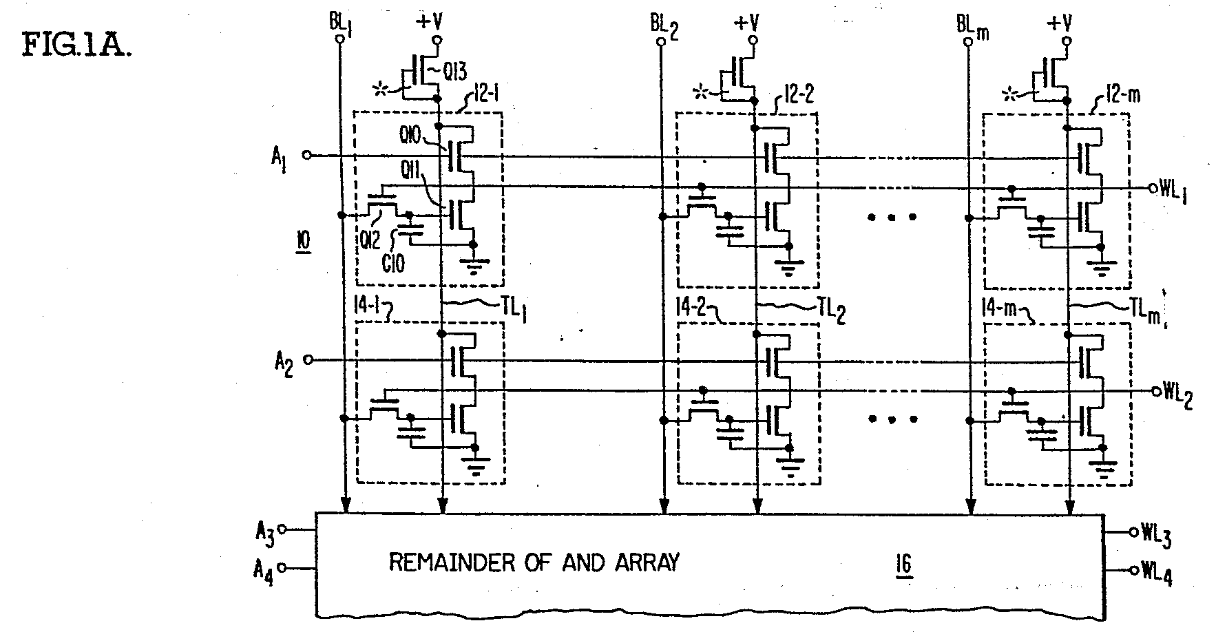
- programmable logic array (PLA) 10 in accordance with the present invention is illustrated in detail.
- Programmable elements 12-1, 12-2...12-m each have a first input terminal coupled to an address line A l and a second input terminal coupled to a word line WL 1 .
- programmable elements 14-1, 14-2...14-m each have a first input terminal coupled to an address line A 2 and a second input terminal coupled to a word line WL 2 .
- Additional programmable elements are similarly coupled to address lines A3, A4, A 5 ...A n and to word lines WL3 , W L 4 , WL 5 ...WL n , which elements are represented by block 16 entitled "Remainder of AND Array".
- the combination of the elements 12-1, 12-2...12-m, 14-1, 14-2...14-m and those represented by the block 16 form what is referred to herein as an AND array of the PLA 10.
- Third and fourth input terminals of each of the elements in each column of the AND array are coupled to bit lines BL 1 , BL 2 ...BL m and term lines TL 1 , TL 2 ...TL m , respectively.
- the address line A 1 is coupled to the gate terminal of a transistor Q10, which transistor has a source terminal coupled to the term line TL 1 .
- the drain terminal of the transistor Q10 is coupled to the source terminal of a transistor Qll, and the drain terminal of this transistor is coupled to ground potential.
- the word line WL 1 is coupled to the gate terminal of a transistor Q12, which transistor has a drain terminal coupled to the bit line BL 1 .
- the source terminal of the transistor Q12 is coupled to the gate terminal of the transistor Qll.
- a storage capacitor C10 is coupled between the source terminal of the transistor Q12 and ground potential.
- the element 12-1 is programmed when a charge is placed on the capacitor C10 by simultaneously applying a high-level (e.g., five volts) signal on the bit line BL 1 and the word line WL l .
- the charge on the capacitor C10 is applied to the gate terminal of the transistor Qll, which will turn on when the transistor Q10 is turned on by a high-level signal on the address line A 1 .
- line TL 1 is coupled to a voltage supply +V (typically five volts) by means of a depletion transistor Q13 connected as a diode (i.e., the gate terminal is tied to the drain terminal of the transistor):
- a depletion transistor Q13 connected as a diode (i.e., the gate terminal is tied to the drain terminal of the transistor):
- the term line TL 1 is held at a high voltage level until it is "pulled down" by one of the programmable elements. More particularly, if the transistors Q10 and Qll are both on, the term line TL 1 is thereby coupled to ground potential (pulled down). This pulling down of the term line is applied to the OR array, which will be described in greater detail hereinbelow.
- the OR array comprises an array of m programmable elements as represented by elements 18-1, 18-2...18-m, and the remaining elements are included in a block 20 entitled "Remainder of OR Array".
- the element 18-1 will be described as representative of the elements of the OR array.
- Output line O 1 is coupled to input terminals of the elements 18-1, 18-2...18-m, and more specifically, is coupled to the source terminal of a transistor Q14 in the element 18-1.
- the gate terminal of Q14 is coupled to the term line TL 1 and the drain terminal is coupled to the source terminal of a transistor Q15.
- Word line WL n+1 is coupled to second input terminals of the elements 18-1, 18-2...18-m, and more specifically is coupled to the gate terminal of a transistor Q 16.
- the source terminal of the transistor Q16 is coupled to the bit line BL 1 , and the drain terminal is coupled to the gate terminal of the transistor Q15.
- a storage capacitor Cll is coupled between the gate terminal of Q15 and ground potential.
- the element 18-1 operates in a manner similar to the above-described element 12-1.
- a charge is placed on the capacitor Cll by simultaneously applying a high-level signal on the bit line BL 1 and the word line WL n+l .
- the charge on the capacitor Cll is applied to the gate terminal of the transistor Q15, which will turn on when the transistor Q14 is turned on by a high-level signal present on the term line TL 1 .
- the output line O 1 is biased at a high level in a manner similar to the term line TL 1 by means of a depletion transistor Q17 connected as a diode to the voltage supply +V.
- the transistor Q14 would be turned off because the term line TL 1 is pulled down to ground potential. In such event, it is irrelevant what charge is present on the capacitor Cll since Q14 is turned off. Hence, in this example, there would be a high level signal on the output line O 1 .
- bit lines BL l , BL 2 ...BL m are coupled to Refresh Logic 22, which logic is of conventional design.
- Refresh Logic 22 is of conventional design.
- a typical refresh logic suitable for Logic 22 is illustrated and described in an article entitled "Peripheral Circuits for One-Transistor Cell MOS RAM's" by F.C. Foss, at page 255 to 261 of the IEEE Journal of Solid State Circuits, Vol. SC-10, No. 5, October, 1975.
- FIG. 2 a logic-schematic diagram of the program register is illustrated.
- Programming data is supplied serially on an input terminal 32 also referred to herein as "SERIAL IN", which terminal is coupled to the data (" D ") input terminal of a flip-flop 30-1.
- the output terminal (“Q") of the flip-flop 30-1 is coupled to the data input terminal of another flip-flop 30-2.
- Additional flip-flops are concatenated together in a conventional manner to form a shift register m units long.
- the clock (CK) terminals of each of the flip-flops of the shift register are coupled to a CK input terminal 34.
- the output terminal of the last flip-flop 30-m of the register is coupled to a "SERIAL OUT" output terminal 36.
- each of the flip-flops 30-1, 30-2, 30-3...30-m is coupled to a source terminal of each of a series of transistors Q20-1, Q20-2, Q20-3...Q20-m, respectively.
- the gate terminals of all of these transistors are connected together at a "LOAD" input terminal 38, and the drain terminals are coupled respectively to each of the'bit lines BL 1 , BL 2 , BL 3 ...BL m .
- THE CK input terminal 40 is coupled to a master clock having a frequency typically between one and four megahertz.
- the terminal 40 is coupled to the input of an inverter 41 of a clock circuit 42 and to the gate terminal of a transistor Q30. It is noted that no more than one or two clock circuits such as circuit 40 are employed for the entire PLA.
- the data "D" input terminal 43 is coupled to the source terminal of Q30, and the drain terminal thereof is coupled to the input of an inverter 44 and one side of a capacitor C30.
- the capacitor C30 is a parasitic capacitor having the other side coupled to ground potential.
- the output of the inverter 44 is coupled to the source terminal of a transistor Q31, and the output of the inverter 41 is coupled to the gate terminal of the same Q31.
- the drain terminal of the transistor Q31 is coupled to the input of an inverter 45 and to one side of a capacitor C31.
- the capacitor C31 is a parasitic capacitor having the other side coupled to ground potential.
- the output of the inverter 45 is coupled to a node Q, which is the output terminal of the flip-flop element.
- a potential (e.g., high-level signal) applied on the terminal 43 is transferred to the input of the inverter 44 by the clock signal applied to the terminal 40 going to a high level.
- This potential is stored by the capacitor C30.
- the output of the inverter 41 goes to a high level and the potential on C30 inverted by the inverter 44 is transferred to the capacitor C31 through Q31.
- the inversion of this potential (now in phase with that on the node D) is supplied at the output node Q.
- the refresh register comprises a series of flip-flops 40-1, 40-2, 40-3...40-n+k.
- the outputs of the flip-flops of the refresh register are coupled to the word lines (WL 1 , WL 2 , WL 3 ...WL n+k ) ⁇
- the clock input terminals of these flip-flops are coupled to a CK input terminal 46.
- the data (“D”) input terminal of the first flip-flop in the series register (i.e., flip-flop 40-1) is coupled to the output of a non-inverting buffer 47, which has a single input terminal coupled to the drain terminals of a pair of transistors Q40 and Q41.
- the gate terminal of the transistor Q40 is coupled to the input of an inverter 48 and to the output terminal of a flip-flop 49.
- the output of the inverter 48 is coupled to the gate terminal of the transistor Q41.
- the data input terminal of the flip-flop 49 is coupled to the output terminal of a flip-flop 50.
- the data input terminal of the flip-flop 50 is coupled to a RESET input terminal 52.
- the clock input terminals of the flip-flops 49 and 50 are coupled to the CK input terminal 46.
- the source terminal of the transistor Q40 is coupled to a voltage supply +V, and the source terminal of the transistor Q41 is coupled to the output terminal of the last flip-flop in the refresh register (i.e., flip-flop 40-n+k).
- the output of the flip-flop 50 which is referred to herein as "RESET A" is coupled to the reset "R" input terminal of each of the flip-flops 40-1, 40-2, 40-3...40-n+k.
- RESET A is supplied to the flip-flops 40-1, 40-2, 40-3 ... 40-n+k, which thereby resets, or restores, the refresh register to a zero state.
- a high level voltage e.g., +5 volts
- a lower voltage e.g., 0 volts
- the flip-flop 49 On the next subsequent clock cycle the flip-flop 49 is set, which provides a "RESET B" signal to the input of the inverter 48 (which causes the transistor Q41 to turn off) and to the gate terminal of the transistor Q40.
- the transistor Q40 turns on and the +V potential (i.e., a logic one) is applied to the data ("D") input terminal of the flip-flop 40-1.
- the logic one On the next clock cycle the logic one is clocked to the flip-flop 40-2, and on the next subsequent clock cycle the same logic one is clocked into the flip-flop 40-3, and so on and so forth.
- the logic one When the logic one is stored in the flip-flop 40-n+k, it is recirculated back to the flip-flop 40-1 by means of the transistor Q41 and the buffer 47.
- the logic one that is being circulated through the refresh register is used to sequentially raise each of the word lines to a high level, which operates in conjunction with the refresh logic 22 to restore the charge programmed on the
- the RESET A signal goes to zero on the clock cycle that set the flip-flop 49.
- the flip-flops 49 and 50 are both reset and the RESET A and RESET B signals are both at a logic zero. Accordingly, the input to the inverter 48 is at a low level, the output thereof is at a high level and the transistor Q41 is turned on. Hence, when the recirculating logic one was applied to the source terminal of the transistor Q41 it was passed therethrough to the input of the flip-flop 40-1.
- Waveform 60 represents a RESET signal that is applied on the terminal 52; waveform 61 represents the RESET A signal appearing at the output of the flip-flop 50; and, waveform 62 represents the RESET B signal appearing at the output of the flip-flop 49.
- Waveforms 63, 64, 65...66 represent the logic one that is being circulated through the refresh register.
- the output of the PLA 10 can be programmed to be inverted, non-inverted or latched by use of program output circuits, one of which is illustrated in FIG. 6.
- a register is employed for storing the output program, which as shown in FIG. 5 comprises flip-flops 70, 71 and 72.
- the register input is the "SERIAL OUT" signal from terminal 36 (FIG. 2) which is coupled to the data ("D") input terminal of the flip-flop 70.
- the outputs of the flip-flops 70, 71 and 72 are coupled to the source terminals of transistors Q50, Q51 and Q52.
- the gate terminals of these transistors are coupled to a LOAD input terminal 74; and the drain terminals are coupled to bit lines BL a , BL b and BL c , respectively, which bit lines are coupled to refresh logic 75.
- a typical output line O x is coupled to the source terminal of a transistor Q53, the input terminal of an inverter 76 and the data ("D") input terminal of a flip-flop 78.
- the clock input terminals of the flip-flops 70, 71, 72 and 78 are coupled to the clock CK input terminal 79.
- the output terminal of the inverter 76 is coupled to the source terminal of a transistor Q54 and the output terminal of the flip-flop 78 is coupled to the source terminal of a transistor Q55.
- the drain terminals of the transistors Q53, Q54 and Q55 are connected together and this connection is coupled to the programmed output "OUT".
- Each of the transistors Q53, Q54 and Q55 are switched on and off by program elements similar to the element 18-1 (FIG. 1) described above.
- the gate terminal of the transistor Q53 is coupled to the drain terminal of a transistor Q56 having a gate terminal coupled to a word line WL x and a source terminal coupled to the bit line BL a .
- a capacitor C51 is coupled between the gate terminal of Q53 and ground for storing a charge.
- the gate terminal of Q54 is coupled to the source terminal of a transistor Q57 having a gate terminal coupled to the word line WL x and a drain terminal coupled to the bit line BL b .
- a capacitor C52 is coupled between the gate terminal of Q54 and ground potential.
- the gate terminal of Q55 is coupled to the source terminal Q58 having a gate terminal coupled to the word line WL x and a drain terminal coupled to the bit line BL c .
- a capacitor C53 is coupled between the gate terminal of Q55 and ground potential.
- the output signal appearing on O x will be transferred through Q53 to the output OUT. If the flip-flop 71 is set and 70 and 72 are reset, the output appearing on O x will be inverted by the inverter 76 and transmitted through Q54 (Q54 is on since flip-flop 71 is set) to the output OUT. In a similar manner, if the flip-flops 70 and 71 are reset and the flip-flop 72 is set, the signal appearing on O x will be latched by the flip-flop 78 on the next clock cycle, and the output thereof will be transmitted through Q55 to the output OUT.
Abstract
Description
- U.S. Patent applications directly or indirectly related to the subject application are the following:
- Serial No. 457,175, filed January 11, 1983 by David W. Page and LuVerne R. Peterson and entitled "A Re-programmable PLA", and
- Serial No. 457,177 , filed January 11, 1983 by David W. Page and entitled "A Dynamic Data Re-programmable PLA".
- This invention relates to programmable logic arrays (PLA's), and more particularly, to PLA's which are readily re-programnable.
- In general, a PLA is a logic circuit which receives a plurality of digital input signals and generates a plurality of digital output signals wherein each of the digital output signals is a programmable sum-of-product combination of the input signals. In conventional PLA's, one circuit is provided for generating a plurality of terms which are the logical AND of selected input signals; and another circuit is provided to generate the output signals by selectively ORing the AND terms. A typical PLA may have a total of n input signals, generate a total of m AND terms from the input signals, and generate a total of k output signals by selectively ORing the m AND terms.
- An article describing PLA's in more detail is "Field-PLA's Simplify Logic Designs", which was published in Electronic Design of September 1, 1975, at pages 84-90. Another series of articles describing PLA's are "Field-programmable Arrays: Powerful Alternatives to Random Logic", Electronics, July 5, 1979, pages 89-94; and "Field-programmable Logic, Part 2: Sequencers and Arrays Transform Truth Tables into Working Systems", Electronics, July 19, 1979, pages 95-102.
- The general design of a PLA includes an AND array feeding into an OR array. The AND array accepts n address inputs which includes an array of terms m deep. Each term is the AND combination of data, or data complement or don't care for each input (don't care is formed by ignoring data and data complement for a given input), hence a typical program may appear as:
- term 1 = A A B
- term 2 = A A B
- term m -
B - The term lines then feed into an OR array where each.term line may be selectively OR'd into an output (the array is m X k where k is the number of outputs).
- The prior art PLA's are typically designed for use in systems requiring permanent or semipermanent nonvolatile logic arrays. PROM's (programmable read only memories) are frequently used to implement logic arrays, which PROM's are usable only once after programming (i.e., the program cannot be changed once made). EPROM's (erasable PROM's) can be changed by the use of an ultraviolet light, which erasure requires several hours to complete. Also, another problem with EPROM's is that they are expensive.
- EEPROM's (electrically erasable PROM's), which are even more expensive than EPROM's, require special power supplies. Furthermore, PROM's are not configured as PLA's.
- An advantage of the present invention resides in the provision of a unique design that is readily adaptable to standard MOS (metal oxide semiconductor) fabrication techniques.
- Another advantage of this invention is the provision of a PLA design that is readily programmable or re-programmable as required, and requires reduced semiconductor chip area ("real estate").
- A programmable logic array is provided which has an AND array disposed for receiving n input signals, an OR array providing k output signals on k output lines and m term lines and m bit lines coupling the AND and OR arrays, wherein the array comprises new and improved random access AND and OR arrays. The AND array includes n X m cells wherein each cell has first and second transistor means coupled in series between one of the term lines and a reference potential. Each cell includes a charge storage element coupled to the control element of the first transistor means and one of the n input terminals is coupled to the control element of the second transistor means. The OR array includes m X k cells wherein each cell has third and fourth transistor means coupled in series between one of said output lines and a reference potential. Each of the OR array cells also includes a charge storage element coupled to the control element of the third transistor means and one of the m term lines is coupled to the control element of the fourth transistor means. Refresh logic is coupled to the bit lines for periodically restoring the charge on the charge storage elements.
-
- FIG. 1 is a schematic diagram of the PLA of this invention;
- FIG. 2 is a logic-schematic diagram of the program register of the PLA;
- FIG. 3 is a schematic diagram of a typical flip-flop employed in this invention;
- FIG. 4 is a logic-schematic diagram of the refresh register of the PLA;
- FIG. 5 is a timing diagram illustrating operation of the PLA; and,
- FIG. 6 is a logic-schematic diagram of a program output circuit of the PLA.
- Referring now to the drawings and in particular to FIG. 1, a programmable logic array (PLA) 10 in accordance with the present invention is illustrated in detail. Programmable elements 12-1, 12-2...12-m each have a first input terminal coupled to an address line Al and a second input terminal coupled to a word line WL1. In a similar manner, programmable elements 14-1, 14-2...14-m each have a first input terminal coupled to an address line A2 and a second input terminal coupled to a word line WL2. Additional programmable elements are similarly coupled to address lines A3, A4, A5...An and to word lines WL3, WL4, WL5...WLn, which elements are represented by
block 16 entitled "Remainder of AND Array". The combination of the elements 12-1, 12-2...12-m, 14-1, 14-2...14-m and those represented by theblock 16 form what is referred to herein as an AND array of thePLA 10. Third and fourth input terminals of each of the elements in each column of the AND array are coupled to bit lines BL1, BL2...BLm and term lines TL1, TL2...TLm, respectively. - Each of the programmable elements in the AND array are formed of the same structural details. The element 12-1 will be described in detail as representative of all such elements in the AND array. The address line A1 is coupled to the gate terminal of a transistor Q10, which transistor has a source terminal coupled to the term line TL1. The drain terminal of the transistor Q10 is coupled to the source terminal of a transistor Qll, and the drain terminal of this transistor is coupled to ground potential. The word line WL1 is coupled to the gate terminal of a transistor Q12, which transistor has a drain terminal coupled to the bit line BL1. The source terminal of the transistor Q12 is coupled to the gate terminal of the transistor Qll. A storage capacitor C10 is coupled between the source terminal of the transistor Q12 and ground potential.
- The element 12-1 is programmed when a charge is placed on the capacitor C10 by simultaneously applying a high-level (e.g., five volts) signal on the bit line BL1 and the word line WLl. The charge on the capacitor C10 is applied to the gate terminal of the transistor Qll, which will turn on when the transistor Q10 is turned on by a high-level signal on the address line A1. At this juncture of the description, it should be noted that the term line TL1 is coupled to a voltage supply +V (typically five volts) by means of a depletion transistor Q13 connected as a diode (i.e., the gate terminal is tied to the drain terminal of the transistor): Hence, the term line TL1 is held at a high voltage level until it is "pulled down" by one of the programmable elements. More particularly, if the transistors Q10 and Qll are both on, the term line TL1 is thereby coupled to ground potential (pulled down). This pulling down of the term line is applied to the OR array, which will be described in greater detail hereinbelow.
- The OR array comprises an array of m programmable elements as represented by elements 18-1, 18-2...18-m, and the remaining elements are included in a
block 20 entitled "Remainder of OR Array"..The element 18-1 will be described as representative of the elements of the OR array. Output line O1 is coupled to input terminals of the elements 18-1, 18-2...18-m, and more specifically, is coupled to the source terminal of a transistor Q14 in the element 18-1. The gate terminal of Q14 is coupled to the term line TL1 and the drain terminal is coupled to the source terminal of a transistor Q15. Word line WLn+1 is coupled to second input terminals of the elements 18-1, 18-2...18-m, and more specifically is coupled to the gate terminal of atransistor Q16. The source terminal of the transistor Q16 is coupled to the bit line BL1, and the drain terminal is coupled to the gate terminal of the transistor Q15. A storage capacitor Cll is coupled between the gate terminal of Q15 and ground potential. - The element 18-1 operates in a manner similar to the above-described element 12-1. A charge is placed on the capacitor Cll by simultaneously applying a high-level signal on the bit line BL1 and the word line WLn+l. The charge on the capacitor Cll is applied to the gate terminal of the transistor Q15, which will turn on when the transistor Q14 is turned on by a high-level signal present on the term line TL1. The output line O1 is biased at a high level in a manner similar to the term line TL1 by means of a depletion transistor Q17 connected as a diode to the voltage supply +V. Thus, if the transistors Q10 and Qll are both on, as described above, the transistor Q14 would be turned off because the term line TL1 is pulled down to ground potential. In such event, it is irrelevant what charge is present on the capacitor Cll since Q14 is turned off. Hence, in this example, there would be a high level signal on the output line O1.
- It should be noted that the bit lines BLl, BL2...BLm are coupled to Refresh
Logic 22, which logic is of conventional design. For example, a typical refresh logic suitable forLogic 22 is illustrated and described in an article entitled "Peripheral Circuits for One-Transistor Cell MOS RAM's" by F.C. Foss, at page 255 to 261 of the IEEE Journal of Solid State Circuits, Vol. SC-10, No. 5, October, 1975. - Referring now to FIG. 2, a logic-schematic diagram of the program register is illustrated. Programming data is supplied serially on an
input terminal 32 also referred to herein as "SERIAL IN", which terminal is coupled to the data ("D") input terminal of a flip-flop 30-1. The output terminal ("Q") of the flip-flop 30-1 is coupled to the data input terminal of another flip-flop 30-2. Additional flip-flops are concatenated together in a conventional manner to form a shift register m units long. The clock (CK) terminals of each of the flip-flops of the shift register are coupled to aCK input terminal 34. The output terminal of the last flip-flop 30-m of the register is coupled to a "SERIAL OUT"output terminal 36. - The output of each of the flip-flops 30-1, 30-2, 30-3...30-m is coupled to a source terminal of each of a series of transistors Q20-1, Q20-2, Q20-3...Q20-m, respectively. The gate terminals of all of these transistors are connected together at a "LOAD" input terminal 38, and the drain terminals are coupled respectively to each of the'bit lines BL1, BL2, BL3...BLm. Hence, when the LOAD signal is at a high level the data in the register are coupled to the bit lines.
- Details of the flip-flop elements used herein, such as elements 30-1, etc., are illustrated in FIG. 3. THE
CK input terminal 40 is coupled to a master clock having a frequency typically between one and four megahertz. The terminal 40 is coupled to the input of an inverter 41 of aclock circuit 42 and to the gate terminal of a transistor Q30. It is noted that no more than one or two clock circuits such ascircuit 40 are employed for the entire PLA. The data "D"input terminal 43 is coupled to the source terminal of Q30, and the drain terminal thereof is coupled to the input of aninverter 44 and one side of a capacitor C30. The capacitor C30 is a parasitic capacitor having the other side coupled to ground potential. - The output of the
inverter 44 is coupled to the source terminal of a transistor Q31, and the output of the inverter 41 is coupled to the gate terminal of the same Q31. The drain terminal of the transistor Q31 is coupled to the input of an inverter 45 and to one side of a capacitor C31. The capacitor C31 is a parasitic capacitor having the other side coupled to ground potential. The output of the inverter 45 is coupled to a node Q, which is the output terminal of the flip-flop element. - In operation, a potential (e.g., high-level signal) applied on the terminal 43 is transferred to the input of the
inverter 44 by the clock signal applied to the terminal 40 going to a high level. This potential is stored by the capacitor C30. When the CK signal drops to a low level, the output of the inverter 41 goes to a high level and the potential on C30 inverted by theinverter 44 is transferred to the capacitor C31 through Q31. The inversion of this potential (now in phase with that on the node D) is supplied at the output node Q. - Referring now to FIG. 4, a logic-schematic diagram of the refresh register and related circuitry is illustrated. The refresh register comprises a series of flip-flops 40-1, 40-2, 40-3...40-n+k. The outputs of the flip-flops of the refresh register are coupled to the word lines (WL1, WL2, WL3...WLn+k)· The clock input terminals of these flip-flops are coupled to a
CK input terminal 46. - The data ("D") input terminal of the first flip-flop in the series register (i.e., flip-flop 40-1) is coupled to the output of a
non-inverting buffer 47, which has a single input terminal coupled to the drain terminals of a pair of transistors Q40 and Q41. The gate terminal of the transistor Q40 is coupled to the input of aninverter 48 and to the output terminal of a flip-flop 49. The output of theinverter 48 is coupled to the gate terminal of the transistor Q41. The data input terminal of the flip-flop 49 is coupled to the output terminal of a flip-flop 50. The data input terminal of the flip-flop 50 is coupled to aRESET input terminal 52. The clock input terminals of the flip-flops CK input terminal 46. - The source terminal of the transistor Q40 is coupled to a voltage supply +V, and the source terminal of the transistor Q41 is coupled to the output terminal of the last flip-flop in the refresh register (i.e., flip-flop 40-n+k). The output of the flip-
flop 50, which is referred to herein as "RESET A", is coupled to the reset "R" input terminal of each of the flip-flops 40-1, 40-2, 40-3...40-n+k. When a RESET signal is applied to the terminal 52, the flip-flop 50 is set on the next subsequent clock cycle. Thus, the RESET A signal is supplied to the flip-flops 40-1, 40-2, 40-3 ... 40-n+k, which thereby resets, or restores, the refresh register to a zero state. It is assumed for discussions herein that a high level voltage (e.g., +5 volts) is a logic one and a lower voltage (e.g., 0 volts) is a logic zero. - On the next subsequent clock cycle the flip-
flop 49 is set, which provides a "RESET B" signal to the input of the inverter 48 (which causes the transistor Q41 to turn off) and to the gate terminal of the transistor Q40. The transistor Q40 turns on and the +V potential (i.e., a logic one) is applied to the data ("D") input terminal of the flip-flop 40-1. On the next clock cycle the logic one is clocked to the flip-flop 40-2, and on the next subsequent clock cycle the same logic one is clocked into the flip-flop 40-3, and so on and so forth. When the logic one is stored in the flip-flop 40-n+k, it is recirculated back to the flip-flop 40-1 by means of the transistor Q41 and thebuffer 47. The logic one that is being circulated through the refresh register is used to sequentially raise each of the word lines to a high level, which operates in conjunction with therefresh logic 22 to restore the charge programmed on the storage capacitors. - When the RESET B signal was generated by setting the flip-
flop 49, the RESET A signal goes to zero on the clock cycle that set the flip-flop 49. On the next following clock cycle, the flip-flops inverter 48 is at a low level, the output thereof is at a high level and the transistor Q41 is turned on. Hence, when the recirculating logic one was applied to the source terminal of the transistor Q41 it was passed therethrough to the input of the flip-flop 40-1. - The operation of the refresh register shown in FIG. 4 can be more fully understood by referring to the timing diagram illustrated in FIG. 5.
Waveform 60 represents a RESET signal that is applied on the terminal 52;waveform 61 represents the RESET A signal appearing at the output of the flip-flop 50; and,waveform 62 represents the RESET B signal appearing at the output of the flip-flop 49.Waveforms - The output of the
PLA 10 can be programmed to be inverted, non-inverted or latched by use of program output circuits, one of which is illustrated in FIG. 6. A register is employed for storing the output program, which as shown in FIG. 5 comprises flip-flops flop 70. The outputs of the flip-flops LOAD input terminal 74; and the drain terminals are coupled to bit lines BLa, BLb and BLc, respectively, which bit lines are coupled to refreshlogic 75. - A typical output line Ox is coupled to the source terminal of a transistor Q53, the input terminal of an
inverter 76 and the data ("D") input terminal of a flip-flop 78. The clock input terminals of the flip-flops CK input terminal 79. The output terminal of theinverter 76 is coupled to the source terminal of a transistor Q54 and the output terminal of the flip-flop 78 is coupled to the source terminal of a transistor Q55. The drain terminals of the transistors Q53, Q54 and Q55 are connected together and this connection is coupled to the programmed output "OUT". - Each of the transistors Q53, Q54 and Q55 are switched on and off by program elements similar to the element 18-1 (FIG. 1) described above. For example, the gate terminal of the transistor Q53 is coupled to the drain terminal of a transistor Q56 having a gate terminal coupled to a word line WLx and a source terminal coupled to the bit line BLa. A capacitor C51 is coupled between the gate terminal of Q53 and ground for storing a charge. Likewise, the gate terminal of Q54 is coupled to the source terminal of a transistor Q57 having a gate terminal coupled to the word line WLx and a drain terminal coupled to the bit line BLb. A capacitor C52 is coupled between the gate terminal of Q54 and ground potential. The gate terminal of Q55 is coupled to the source terminal Q58 having a gate terminal coupled to the word line WLx and a drain terminal coupled to the bit line BLc. A capacitor C53 is coupled between the gate terminal of Q55 and ground potential.
- The operation of this circuit is similar to that described above with reference to the element 18-1 (FIG. 1). Assume the flip-
flop 70 is set and flip-flops flop 71 is set and 70 and 72 are reset, the output appearing on Ox will be inverted by theinverter 76 and transmitted through Q54 (Q54 is on since flip-flop 71 is set) to the output OUT. In a similar manner, if the flip-flops flop 72 is set, the signal appearing on Ox will be latched by the flip-flop 78 on the next clock cycle, and the output thereof will be transmitted through Q55 to the output OUT. - It may be appreciated from the description above that a dynamic re-programmable logic array has been described in detail. Thus, while the invention has been particularly shown and described in detail with reference to only one embodiment, it will be understood by those skilled in the art that the foregoing and other changes in form and details may be made without departing from the spirit and scope of the invention. Accordingly, it is intended that the present invention only be limited by the appended claims.
Claims (16)
Applications Claiming Priority (2)
| Application Number | Priority Date | Filing Date | Title |
|---|---|---|---|
| US06/457,176 US4546273A (en) | 1983-01-11 | 1983-01-11 | Dynamic re-programmable PLA |
| US457176 | 1983-01-11 |
Publications (2)
| Publication Number | Publication Date |
|---|---|
| EP0116287A2 true EP0116287A2 (en) | 1984-08-22 |
| EP0116287A3 EP0116287A3 (en) | 1986-05-07 |
Family
ID=23815739
Family Applications (1)
| Application Number | Title | Priority Date | Filing Date |
|---|---|---|---|
| EP84100235A Withdrawn EP0116287A3 (en) | 1983-01-11 | 1984-01-11 | Dynamic re-programmable pla |
Country Status (3)
| Country | Link |
|---|---|
| US (1) | US4546273A (en) |
| EP (1) | EP0116287A3 (en) |
| JP (1) | JPS59161129A (en) |
Cited By (8)
| Publication number | Priority date | Publication date | Assignee | Title |
|---|---|---|---|---|
| GB2184878A (en) * | 1985-02-14 | 1987-07-01 | Intel Corp | Software programmable logic array |
| EP0282256A2 (en) * | 1987-03-06 | 1988-09-14 | Altera Corporation | Micro-sequencer device |
| EP0289035A2 (en) * | 1987-04-30 | 1988-11-02 | Oki Electric Industry Company, Limited | MOS Gate array device |
| FR2652462A1 (en) * | 1989-09-28 | 1991-03-29 | Bull Sa | INTEGRATED PROGRAMMABLE LOGIC NETWORK. |
| DE19525758A1 (en) * | 1994-07-14 | 1996-01-25 | Hyundai Electronics Ind | Reprogrammable programmable logic array |
| US5555214A (en) * | 1995-11-08 | 1996-09-10 | Altera Corporation | Apparatus for serial reading and writing of random access memory arrays |
| US7815933B2 (en) | 2001-09-07 | 2010-10-19 | Nicox S.A. | Self emulsifying drug delivery system |
| US10453846B2 (en) | 2010-09-13 | 2019-10-22 | Semiconductor Energy Laboratory Co., Ltd. | Semiconductor device |
Families Citing this family (50)
| Publication number | Priority date | Publication date | Assignee | Title |
|---|---|---|---|---|
| US4774421A (en) * | 1984-05-03 | 1988-09-27 | Altera Corporation | Programmable logic array device using EPROM technology |
| JPS61170828A (en) * | 1985-01-24 | 1986-08-01 | Hitachi Ltd | Microprogram control device |
| US4787047A (en) * | 1985-03-22 | 1988-11-22 | Intersil | Electrically erasable fused programmable logic array |
| JPH0787032B2 (en) * | 1985-07-08 | 1995-09-20 | 日本電気アイシ−マイコンシステム株式会社 | Semiconductor memory device |
| FR2587516B1 (en) * | 1985-09-13 | 1987-11-20 | Eurotechnique Sa | INSTRUCTION SEQUENCER FOR MICROPROCESSOR WITH NETWORK ARCHITECTURE |
| US4876640A (en) * | 1986-02-07 | 1989-10-24 | Advanced Micro Devices, Inc. | Logic controller having programmable logic "and" array using a programmable gray-code counter |
| US4779229A (en) * | 1986-07-02 | 1988-10-18 | Advanced Micro Devices, Inc. | Prom with programmable output structures |
| US4791603A (en) * | 1986-07-18 | 1988-12-13 | Honeywell Inc. | Dynamically reconfigurable array logic |
| US4730130A (en) * | 1987-01-05 | 1988-03-08 | Motorola, Inc. | Writable array logic |
| EP0312142B1 (en) * | 1987-10-12 | 1992-09-02 | Koninklijke Philips Electronics N.V. | Read circuit for a delay circuit |
| US5007022A (en) * | 1987-12-21 | 1991-04-09 | Texas Instruments Incorporated | Two-port two-transistor DRAM |
| US4894805A (en) * | 1988-04-28 | 1990-01-16 | Eastman Kodak Company | Security printer/copier |
| EP0469393B1 (en) * | 1990-07-30 | 1999-10-06 | Texas Instruments Incorporated | Static random access array including at least one arithmetic and logic unit |
| CA2158467A1 (en) * | 1993-03-17 | 1994-09-29 | Richard D. Freeman | Random access memory (ram) based configurable arrays |
| US5317212A (en) * | 1993-03-19 | 1994-05-31 | Wahlstrom Sven E | Dynamic control of configurable logic |
| US5815726A (en) * | 1994-11-04 | 1998-09-29 | Altera Corporation | Coarse-grained look-up table architecture |
| US5821773A (en) * | 1995-09-06 | 1998-10-13 | Altera Corporation | Look-up table based logic element with complete permutability of the inputs to the secondary signals |
| US5729495A (en) * | 1995-09-29 | 1998-03-17 | Altera Corporation | Dynamic nonvolatile memory cell |
| US5869979A (en) * | 1996-04-05 | 1999-02-09 | Altera Corporation | Technique for preconditioning I/Os during reconfiguration |
| US5977791A (en) * | 1996-04-15 | 1999-11-02 | Altera Corporation | Embedded memory block with FIFO mode for programmable logic device |
| US5859544A (en) * | 1996-09-05 | 1999-01-12 | Altera Corporation | Dynamic configurable elements for programmable logic devices |
| US6191611B1 (en) | 1997-10-16 | 2001-02-20 | Altera Corporation | Driver circuitry for programmable logic devices with hierarchical interconnection resources |
| US6184707B1 (en) | 1998-10-07 | 2001-02-06 | Altera Corporation | Look-up table based logic element with complete permutability of the inputs to the secondary signals |
| DE19860390A1 (en) * | 1998-12-28 | 2000-06-29 | Deutsche Telekom Ag | Programmable logic device uses logic arrays providing programmable AND plane and programmable OR plane in combination with memory or shift register cells |
| US6798693B2 (en) | 2001-09-18 | 2004-09-28 | Kilopass Technologies, Inc. | Semiconductor memory cell and memory array using a breakdown phenomena in an ultra-thin dielectric |
| JP4599059B2 (en) * | 2001-09-18 | 2010-12-15 | キロパス テクノロジー インコーポレイテッド | Semiconductor memory cell and memory array utilizing breakdown phenomenon of ultra-thin dielectric |
| US6700151B2 (en) * | 2001-10-17 | 2004-03-02 | Kilopass Technologies, Inc. | Reprogrammable non-volatile memory using a breakdown phenomena in an ultra-thin dielectric |
| US6693453B1 (en) * | 2002-04-23 | 2004-02-17 | Macronix International Co., Ltd. | Re-programmable logic array |
| US6992925B2 (en) * | 2002-04-26 | 2006-01-31 | Kilopass Technologies, Inc. | High density semiconductor memory cell and memory array using a single transistor and having counter-doped poly and buried diffusion wordline |
| US6940751B2 (en) * | 2002-04-26 | 2005-09-06 | Kilopass Technologies, Inc. | High density semiconductor memory cell and memory array using a single transistor and having variable gate oxide breakdown |
| US6777757B2 (en) * | 2002-04-26 | 2004-08-17 | Kilopass Technologies, Inc. | High density semiconductor memory cell and memory array using a single transistor |
| US6898116B2 (en) * | 2002-04-26 | 2005-05-24 | Kilopass Technologies, Inc. | High density semiconductor memory cell and memory array using a single transistor having a buried N+ connection |
| US6650143B1 (en) * | 2002-07-08 | 2003-11-18 | Kilopass Technologies, Inc. | Field programmable gate array based upon transistor gate oxide breakdown |
| US7042772B2 (en) * | 2002-09-26 | 2006-05-09 | Kilopass Technology, Inc. | Methods and circuits for programming of a semiconductor memory cell and memory array using a breakdown phenomenon in an ultra-thin dielectric |
| US7031209B2 (en) * | 2002-09-26 | 2006-04-18 | Kilopass Technology, Inc. | Methods and circuits for testing programmability of a semiconductor memory cell and memory array using a breakdown phenomenon in an ultra-thin dielectric |
| US6791891B1 (en) | 2003-04-02 | 2004-09-14 | Kilopass Technologies, Inc. | Method of testing the thin oxide of a semiconductor memory cell that uses breakdown voltage |
| US6924664B2 (en) * | 2003-08-15 | 2005-08-02 | Kilopass Technologies, Inc. | Field programmable gate array |
| US7064973B2 (en) | 2004-02-03 | 2006-06-20 | Klp International, Ltd. | Combination field programmable gate array allowing dynamic reprogrammability |
| US6972986B2 (en) * | 2004-02-03 | 2005-12-06 | Kilopass Technologies, Inc. | Combination field programmable gate array allowing dynamic reprogrammability and non-votatile programmability based upon transistor gate oxide breakdown |
| US20050218929A1 (en) * | 2004-04-02 | 2005-10-06 | Man Wang | Field programmable gate array logic cell and its derivatives |
| JP4981661B2 (en) * | 2004-05-06 | 2012-07-25 | サイデンス コーポレーション | Split channel antifuse array structure |
| US9123572B2 (en) | 2004-05-06 | 2015-09-01 | Sidense Corporation | Anti-fuse memory cell |
| US8735297B2 (en) | 2004-05-06 | 2014-05-27 | Sidense Corporation | Reverse optical proximity correction method |
| US7755162B2 (en) * | 2004-05-06 | 2010-07-13 | Sidense Corp. | Anti-fuse memory cell |
| US20050275427A1 (en) * | 2004-06-10 | 2005-12-15 | Man Wang | Field programmable gate array logic unit and its cluster |
| US7164290B2 (en) * | 2004-06-10 | 2007-01-16 | Klp International, Ltd. | Field programmable gate array logic unit and its cluster |
| US7135886B2 (en) * | 2004-09-20 | 2006-11-14 | Klp International, Ltd. | Field programmable gate arrays using both volatile and nonvolatile memory cell properties and their control |
| US7193436B2 (en) * | 2005-04-18 | 2007-03-20 | Klp International Ltd. | Fast processing path using field programmable gate array logic units |
| US8661394B1 (en) | 2008-09-24 | 2014-02-25 | Iowa State University Research Foundation, Inc. | Depth-optimal mapping of logic chains in reconfigurable fabrics |
| US8438522B1 (en) | 2008-09-24 | 2013-05-07 | Iowa State University Research Foundation, Inc. | Logic element architecture for generic logic chains in programmable devices |
Citations (1)
| Publication number | Priority date | Publication date | Assignee | Title |
|---|---|---|---|---|
| EP0005847A1 (en) * | 1978-06-05 | 1979-12-12 | International Business Machines Corporation | Memory circuit and its use in an electrically programmable logic array |
Family Cites Families (9)
| Publication number | Priority date | Publication date | Assignee | Title |
|---|---|---|---|---|
| US3718915A (en) * | 1971-06-07 | 1973-02-27 | Motorola Inc | Opposite conductivity gating circuit for refreshing information in semiconductor memory cells |
| US3758761A (en) * | 1971-08-17 | 1973-09-11 | Texas Instruments Inc | Self-interconnecting/self-repairable electronic systems on a slice |
| DE2455178C2 (en) * | 1974-11-21 | 1982-12-23 | Siemens AG, 1000 Berlin und 8000 München | Integrated, programmable logic arrangement |
| IT1041882B (en) * | 1975-08-20 | 1980-01-10 | Honeywell Inf Systems | SEMICONDUCTOR DYNAMIC MEMORY AND RELATIVE RECHARGE SYSTEM |
| US4203159A (en) * | 1978-10-05 | 1980-05-13 | Wanlass Frank M | Pseudostatic electronic memory |
| US4415818A (en) * | 1979-01-16 | 1983-11-15 | Nippon Telegraph & Telephone Corp. | Programmable sequential logic circuit devices |
| GB2049958B (en) * | 1979-03-15 | 1983-11-30 | Nippon Electric Co | Integrated logic circuit adapted to performance tests |
| JPS57129537A (en) * | 1981-02-05 | 1982-08-11 | Toshiba Corp | Programmable array circuit |
| US4442508A (en) * | 1981-08-05 | 1984-04-10 | General Instrument Corporation | Storage cells for use in two conductor data column storage logic arrays |
-
1983
- 1983-01-11 US US06/457,176 patent/US4546273A/en not_active Expired - Lifetime
-
1984
- 1984-01-10 JP JP59003345A patent/JPS59161129A/en active Pending
- 1984-01-11 EP EP84100235A patent/EP0116287A3/en not_active Withdrawn
Patent Citations (1)
| Publication number | Priority date | Publication date | Assignee | Title |
|---|---|---|---|---|
| EP0005847A1 (en) * | 1978-06-05 | 1979-12-12 | International Business Machines Corporation | Memory circuit and its use in an electrically programmable logic array |
Non-Patent Citations (1)
| Title |
|---|
| IBM TECHNICAL DISCLOSURE BULLETIN, vol. 24, no. 5, October 1981, pages 2424,2425, Armonk, New York, US; T. WINLOW: "Reloadable programmable logic array" * |
Cited By (14)
| Publication number | Priority date | Publication date | Assignee | Title |
|---|---|---|---|---|
| GB2184878A (en) * | 1985-02-14 | 1987-07-01 | Intel Corp | Software programmable logic array |
| GB2184878B (en) * | 1985-02-14 | 1989-11-01 | Intel Corp | Software programmable logic array |
| EP0282256A2 (en) * | 1987-03-06 | 1988-09-14 | Altera Corporation | Micro-sequencer device |
| EP0282256A3 (en) * | 1987-03-06 | 1989-11-02 | Altera Corporation | Micro-sequencer device |
| EP0289035A2 (en) * | 1987-04-30 | 1988-11-02 | Oki Electric Industry Company, Limited | MOS Gate array device |
| EP0289035B1 (en) * | 1987-04-30 | 1994-02-09 | Oki Electric Industry Company, Limited | MOS Gate array device |
| EP0420752A1 (en) * | 1989-09-28 | 1991-04-03 | Bull S.A. | Integrated programmable logic array |
| US5086240A (en) * | 1989-09-28 | 1992-02-04 | Bull S.A. | Programmable integrated logic network having bipolar and mos transistors |
| FR2652462A1 (en) * | 1989-09-28 | 1991-03-29 | Bull Sa | INTEGRATED PROGRAMMABLE LOGIC NETWORK. |
| DE19525758A1 (en) * | 1994-07-14 | 1996-01-25 | Hyundai Electronics Ind | Reprogrammable programmable logic array |
| US5555214A (en) * | 1995-11-08 | 1996-09-10 | Altera Corporation | Apparatus for serial reading and writing of random access memory arrays |
| USRE37060E1 (en) | 1995-11-08 | 2001-02-20 | Altera Corporation | Apparatus for serial reading and writing of random access memory arrays |
| US7815933B2 (en) | 2001-09-07 | 2010-10-19 | Nicox S.A. | Self emulsifying drug delivery system |
| US10453846B2 (en) | 2010-09-13 | 2019-10-22 | Semiconductor Energy Laboratory Co., Ltd. | Semiconductor device |
Also Published As
| Publication number | Publication date |
|---|---|
| EP0116287A3 (en) | 1986-05-07 |
| JPS59161129A (en) | 1984-09-11 |
| US4546273A (en) | 1985-10-08 |
Similar Documents
| Publication | Publication Date | Title |
|---|---|---|
| US4546273A (en) | Dynamic re-programmable PLA | |
| US5859544A (en) | Dynamic configurable elements for programmable logic devices | |
| US6532169B1 (en) | SONOS latch and application | |
| US4508977A (en) | Re-programmable PLA | |
| US5535160A (en) | Semiconductor integrated circuit | |
| KR0172366B1 (en) | Non-volatile semiconductor memory device | |
| KR100328161B1 (en) | Integrated circuit memory | |
| US5243573A (en) | Sense amplifier for nonvolatile semiconductor storage devices | |
| US4603405A (en) | Monolithically integrated semiconductor circuit | |
| EP0162083B1 (en) | Glitch lockout circuit for memory array | |
| KR960001327B1 (en) | Dynamic random access memory device with built-in test mode | |
| EP0051920B1 (en) | Memory arrangement with means for interfacing a central processing unit | |
| US4327424A (en) | Read-only storage using enhancement-mode, depletion-mode or omitted gate field-effect transistors | |
| US4449203A (en) | Memory with reference voltage generator | |
| US4524430A (en) | Dynamic data re-programmable PLA | |
| US3644907A (en) | Complementary mosfet memory cell | |
| EP0121394A2 (en) | Static semiconductor memory device incorporating redundancy memory cells | |
| US5818758A (en) | Zero voltage drop negative switch for dual well processes | |
| US5999459A (en) | High-performance pass-gate isolation circuitry | |
| EP0115140B1 (en) | Decoder circuit | |
| US5563837A (en) | Semiconductor memory device with reduced consumption power and refreshing method of the same | |
| US5999461A (en) | Low voltage bootstrapping circuit | |
| JP2003233996A (en) | Semiconductor memory device | |
| KR100465068B1 (en) | Pumping circuit | |
| US5416737A (en) | MOS memory unit for serial information processing |
Legal Events
| Date | Code | Title | Description |
|---|---|---|---|
| PUAI | Public reference made under article 153(3) epc to a published international application that has entered the european phase |
Free format text: ORIGINAL CODE: 0009012 |
|
| AK | Designated contracting states |
Designated state(s): BE DE FR GB NL SE |
|
| RAP1 | Party data changed (applicant data changed or rights of an application transferred) |
Owner name: BURROUGHS CORPORATION (A DELAWARE CORPORATION) |
|
| PUAL | Search report despatched |
Free format text: ORIGINAL CODE: 0009013 |
|
| AK | Designated contracting states |
Kind code of ref document: A3 Designated state(s): BE DE FR GB NL SE |
|
| 17P | Request for examination filed |
Effective date: 19860818 |
|
| 17Q | First examination report despatched |
Effective date: 19880310 |
|
| STAA | Information on the status of an ep patent application or granted ep patent |
Free format text: STATUS: THE APPLICATION IS DEEMED TO BE WITHDRAWN |
|
| 18D | Application deemed to be withdrawn |
Effective date: 19880721 |
|
| RIN1 | Information on inventor provided before grant (corrected) |
Inventor name: OSMAN, FAZIL ISMET |