EP0116275A2 - Reactive power compensator - Google Patents
Reactive power compensator Download PDFInfo
- Publication number
- EP0116275A2 EP0116275A2 EP84100127A EP84100127A EP0116275A2 EP 0116275 A2 EP0116275 A2 EP 0116275A2 EP 84100127 A EP84100127 A EP 84100127A EP 84100127 A EP84100127 A EP 84100127A EP 0116275 A2 EP0116275 A2 EP 0116275A2
- Authority
- EP
- European Patent Office
- Prior art keywords
- capacitor
- discharge circuit
- voltage
- thyristor switch
- reactive power
- Prior art date
- Legal status (The legal status is an assumption and is not a legal conclusion. Google has not performed a legal analysis and makes no representation as to the accuracy of the status listed.)
- Granted
Links
Images

Classifications
-
- H—ELECTRICITY
- H02—GENERATION; CONVERSION OR DISTRIBUTION OF ELECTRIC POWER
- H02J—CIRCUIT ARRANGEMENTS OR SYSTEMS FOR SUPPLYING OR DISTRIBUTING ELECTRIC POWER; SYSTEMS FOR STORING ELECTRIC ENERGY
- H02J3/00—Circuit arrangements for ac mains or ac distribution networks
- H02J3/18—Arrangements for adjusting, eliminating or compensating reactive power in networks
- H02J3/1821—Arrangements for adjusting, eliminating or compensating reactive power in networks using shunt compensators
- H02J3/1835—Arrangements for adjusting, eliminating or compensating reactive power in networks using shunt compensators with stepless control
- H02J3/1864—Arrangements for adjusting, eliminating or compensating reactive power in networks using shunt compensators with stepless control wherein the stepless control of reactive power is obtained by at least one reactive element connected in series with a semiconductor switch
-
- Y—GENERAL TAGGING OF NEW TECHNOLOGICAL DEVELOPMENTS; GENERAL TAGGING OF CROSS-SECTIONAL TECHNOLOGIES SPANNING OVER SEVERAL SECTIONS OF THE IPC; TECHNICAL SUBJECTS COVERED BY FORMER USPC CROSS-REFERENCE ART COLLECTIONS [XRACs] AND DIGESTS
- Y02—TECHNOLOGIES OR APPLICATIONS FOR MITIGATION OR ADAPTATION AGAINST CLIMATE CHANGE
- Y02E—REDUCTION OF GREENHOUSE GAS [GHG] EMISSIONS, RELATED TO ENERGY GENERATION, TRANSMISSION OR DISTRIBUTION
- Y02E40/00—Technologies for an efficient electrical power generation, transmission or distribution
- Y02E40/10—Flexible AC transmission systems [FACTS]
Definitions
- the invention is based on a reactive power compensator according to the preamble of patent claim 1.
- the invention relates to a prior art of reactive power compensators, as described in DE-PS 23 03 939.
- a compensation capacitor is precharged to the peak value of the mains AC voltage in the quarter period of the AC voltage preceding the switch-on time and connected to the AC network to be compensated by means of a thyristor switch via a choke when the voltage at the thyristor switch is approximately 0.
- the capacitor is discharged by firing the thyristor switch.
- the thyristor switch is closed, that is to say electrically conductive, and thus the capacitor AC network switched on, the voltage across the capacitor corresponds to the mains voltage at all times.
- the thyristor switch takes over the capacitor voltage at the time of switching and subsequently, with the change in the capacitor voltage and the mains voltage, the differential voltage from both.
- the capacitor voltage decreases at least on average over time due to the discharge of the capacitor via the discharge circuit connected in parallel with it.
- the capacitor is disconnected from the AC network at zero current crossing, ie at the maximum mains voltage. If the discharge of the capacitor via the discharge circuit is a slow process compared to the period of oscillation of the AC voltage, then after half a period of oscillation, the thyristor switch practically shows twice the maximum mains voltage.
- the capacitor In order to have to dimension the thyristor switch only for a simple maximum mains voltage, which is of considerable advantage for economic reasons, the capacitor must be able to discharge quickly enough via its discharge circuit, at the longest during half a period of the alternating voltage.
- the duration of half a period is 10 ms at an AC voltage frequency of 50 Hz.
- the capacitor usually has a capacitance on the order of a few 100 uF.
- the discharge circuit In order for such a large capacity to discharge in 10 ms, the discharge circuit must have a low resistance.
- a purely ohmic resistance in the discharge circuit should be, for example, only a few ⁇ , which for the capacitor practically represents a short circuit with a correspondingly high power loss, which cannot be tolerated when the capacitor is connected to the AC voltage.
- This power loss can be limited by a switch arranged in the discharge circuit, primarily a fast-acting semiconductor switch is open during the connection of the capacitor to the AC network and is only closed when the capacitor is disconnected from the AC network to initiate the discharge.
- a switch arranged in the discharge circuit, primarily a fast-acting semiconductor switch is open during the connection of the capacitor to the AC network and is only closed when the capacitor is disconnected from the AC network to initiate the discharge.
- Such a switch must be dimensioned for the full maximum mains voltage and is therefore also economically complex.
- the invention solves the problem of specifying a reactive power compensator which is subjected to low voltage loads and does not require any switching elements in the discharge circuit of the compensation capacitor.
- An advantage of the invention is that a rapid and continuous discharge of the capacitor, after it has been switched off from the AC voltage network, takes place in the discharge circuit of the capacitor without any fault-prone and expensive switching elements. This is achieved with simple means.
- a specially dimensioned iron choke coil can be used, with a second winding possibly also is provided for a particularly rapid magnetic reversal of the iron core.
- a specially dimensioned transformer with a short-circuit switch in its secondary circuit can also be used, which also enables very fast magnetic reversal and thus rapid discharge of the reactive load capacitor. This ensures that the valve voltage is relatively low and thus costs for expensive high voltage thyristors are saved.
- the destruction of thyristor valves can be avoided with certainty even in the event of a double misfire.
- N denotes a line of an electrical AC voltage network which is fed by a generator G.
- a reactive power capacitor C Connected to network N. is a reactive power capacitor C in series with a thyristor switch TS built up, for example, from anti-parallel thyristors.
- the ignition electrodes of the thyristors of the thyristor switch TS are connected to a first control unit SE 1 . These are derived as input values from the alternating-voltage network N electric current, V oltage and frequency signals M i, M u, M ⁇ supplied.
- the first control unit SE 1 From these signals, the first control unit SE 1 generates ignition pulses for the thyristors of the thyristor switch TS in a manner known per se and therefore also not explained in more detail if required for reactive power in the AC voltage network N.
- the capacitor C is connected in parallel with a discharge circuit which, as a variable reactance, has a discharge circuit choke D provided with an iron core.
- the ohmic effective resistance of the choke winding is denoted by R and is shown separately from the discharge circuit choke D.
- the capacitor C forms a resonant circuit together with the discharge circuit reactor D. If this is a parallel resonant circuit in series with the thyristor switch TS N. on the alternating-voltage network of the thyristor switch TS is closed, at least one of the two shown in Fig. Antiparallel thyristors after the ignition by the first control unit SE 1 1-conductive, so the parallel resonant circuit is an oscillation with the Frequency of the AC voltage in the AC network N, ie the network frequency ⁇ N is forced.
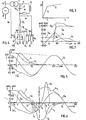
- FIG. 3 shows the magnetization characteristic of the iron core of the discharge circuit dossel D.
- the induction flow. is plotted against the current i 2 through the discharge circuit choke D and, idealized to a great extent, is composed of two straight sections designated 1 and 2. With small current values, the induction flow increases steeply (straight section 1). In this area the iron core is unsaturated and the inductance of the discharge circuit choke D, which results from the slope of the straight section, is large. The iron core is saturated at a saturation current value i S. The induction flux e increases only slowly above this saturation current value i s .
- the aim should be to make the straight section 1 as steep as possible and to make the straight section 2 as flat as possible.
- the former can be achieved, among other things, by using a self-contained, approximately toroidal iron core. This largely eliminates the scattering of the induction flux ⁇ .
- the latter can be achieved, among other things, by an even distribution of the choke winding over the iron core. As a result, the ratio of the number of turns to the length of the discharge circuit choke D, which also determines the size of the air inductance, is minimal.
- the saturation flow is preferably dimensioned to approximately 1.3 times the flow which flows through the discharge circuit choke D with the mains frequency ⁇ N when the capacitor C is connected to the AC voltage network N.
- the saturation property of the discharge circuit choke D only comes into play as soon as the capacitor C is separated from the AC voltage network N by opening the thyristor switch TS. From this point in time, the oscillating circuit comprising capacitor C and discharge circuit choke D is no longer forced to oscillate at the mains frequency ⁇ N specified by the AC network N.
- the resonant circuit oscillates freely with its own frequency, ie its natural frequency ⁇ E , which is determined by the capacitance of the capacitor C, the inductance of the unsaturated discharge circuit reactor D and the ohmic resistor R, is further damped.
- the choke represents a smaller resistance for the free, damped oscillation than for the forced oscillation with the mains frequency ⁇ N. Since the capacitor C is disconnected from the AC voltage network N at the maximum line voltage, the maximum line voltage U N is also present at the capacitor C as the initial value of the free damped oscillation. Under these conditions, the current through the discharge circuit choke D in the free, damped oscillation considerably exceeds the current of the forced oscillation and drives the iron core of the discharge circuit choke D into saturation.
- the damping resistance R of the winding of the discharge circuit inductor D is preferably chosen so that the discharge of the capacitor corresponds to an RC discharge with aperiodic damping, with where L means the inductance of the discharge circuit choke D in the saturated region.
- the ohmic resistance R is preferably the effective resistance of the winding of the discharge circuit inductor D, for which, for example, a material with a higher specific resistance than copper or aluminum is used.
- the discharge circuit inductor D acts as a variable reactance due to the saturation property of its iron core in the discharge circuit, which is larger when the capacitor C is connected to the AC network N, that is to say when the thyristor switch TS is closed, than when the capacitor C is at open thyristor switch TS is separated from the AC network N.
- the difference between these two states is so significant that in the former case only a small, insignificant current i 2 flows in the discharge circuit, while in the second case a large current, which discharges the capacitor C in less than half a period of the AC voltage i 2 can flow.
- the discharge circuit can also be permanently closed. An interruption of the discharge circuit during the connection of the capacitor C to the AC network N is not necessary.
- An additional winding ZW is advantageously placed around the iron core of an unloading circuit choke D, as shown in FIG. 1, to which a device E for accelerated magnetic reversal of the iron core is connected. This is connected via a control line SY for synchronization with the first control unit SE 1 .
- the time period that elapses after the capacitor C is disconnected from the AC voltage network N and the free, damped oscillation sets in, until the current in the discharge circuit choke D has risen to such an extent that saturation occurs.
- a transformer TR is provided in the discharge circuit as a variable reactance. This is connected to the discharge circuit with a primary side.
- a controllable switching element SS is arranged in the secondary circuit of the transformer TR. With the controllable switching element SS, the secondary circuit of the transformer TR can be short-circuited and opened.
- the controllable switching element SS is preferably constructed from anti-parallel thyristors.
- the controllable switching element SS is assigned a second control unit SE 2 , which, like the first control unit SE 1 , generates ignition pulses for the thyristors. For synchronization, a second control unit SE 2 is coupled to the first control unit SE 1 .
- the second control unit SE 2 generates precisely then ignition pulses for the thyristors of the controllable switching element SS when the first control unit SE 1 is not generating any ignition pulses for the thyristors of the thyristor switch TS and vice versa.
- the second control unit SE 2 therefore only needs to negate the control signal of the first control unit SE 1 . This ensures that the controllable switching element SS is always open or closed in the opposite direction to the thyristor switch TS.
- This embodiment of the invention takes advantage of the fact that with an open secondary circuit of the transformer TR, the full inductance of the primary winding, the so-called no-load inductance, is effective in its primary circuit, whereas the so-called short-circuit or leakage impedance of the transformer is effective when the secondary circuit is closed.
- the transformer TR consequently acts with an open secondary circuit as a large reactance in the discharge circuit (during the connection of the capacitor C to the AC network), so that only a small current i 2 can flow in the discharge circuit, as explained above for the discharge circuit reactor D.
- the transformer TR acts as a small reactance (if the capacitor is disconnected from the AC network N), so that, as also explained above for the discharge circuit choke, the capacitor C can quickly discharge through a free, damped oscillation.
- a switching element in the discharge circuit is unnecessary.
- the controllable switching element SS in the secondary circuit of the transformer TR offers the great advantage over a switching element in the discharge circuit that it only needs to be designed for a down-transformed and therefore much lower secondary voltage of the transformer TR.
- the capacitor C is connected to the AC network N via a transformer T.
- the discharge circuit reactor D is again connected with its active resistance R.
- an air throttle D L is connected to limit the valve current i TS in transient processes, the effective resistance of which is denoted by R L.
- the thyristor switch TS has two antiparallel connected thyristors V 1 and V 2 in parallel to a wiring capacitor B K.
- i TS and U TS denote the valve current and the valve voltage at the thyristor switch TS.
- a first varistor or overvoltage arrester A 1 is connected in parallel with the series circuit comprising air throttle D 1 and thyristor switch TS, and a second varistor or overvoltage arrester A 2 is connected in parallel with the thyristor switch TS.
- Both surge arresters A 1 and A 2 are voltage-dependent resistors made of a metal oxide, preferably zinc oxide, whose resistance value decreases with increasing voltage from a predefinable level of protection or protective voltage value.
- the level of protection of the first surge arrester A 1 is preferably greater than twice the amplitude of the mains voltage U N , which occurs on the secondary or low voltage side of the transformer T.
- the level of protection of the second surge arrester A 2 is preferably the same or greater than the level of protection of the first surge arrester A 1 ; In terms of performance, however, the second surge arrester A 2 is designed to be weaker than the first surge arrester A 1 .
- the currents through the surge arresters A 1 and A 2 are denoted by i Al and i A2 , and the voltage drops occurring during current passage are denoted by U A1 and U A2 .
- FIG. 4 The effect of the circuit according to FIG. 4 is explained below with reference to FIGS. 5 to 7, in which the current i in kA and the voltage U in kV are plotted on the ordinate and the time t in ms is plotted on the abscissa (FIGS. 5 and 6) or in a us (Fig. 7).
- FIG. 5 shows when the compensation capacitor is switched off, the time profile of the sinusoidal mains voltage U N , the voltage U c of the reactive power capacitor C, the valve voltage U TS and the capacitor discharge current i 2 for the undisturbed case.
- the following applies to the valve voltage U TS From the switch-off instant t 0 of the thyristor switch TS to the instant t 1 at which the iron core of the discharge circuit choke D saturates, the capacitor voltage U c is approximately constant and the capacitor discharge current i 2 is low, due to the high resistance of the discharge circuit choke D. Thereafter, the capacitor discharge current i 2 rises sharply and discharges the capacitor C within a half-oscillation of the mains frequency ⁇ n .
- the maximum valve voltage U TS is only about 15% higher than the mains voltage amplitude.
- the capacitor C would discharge only very slowly, in accordance with the line shown in broken lines in FIG. 5. This would have the consequence that at the time of the minimum of the mains voltage UN, the valve voltage U TS would be approximately twice as large as the mains voltage amplitude. Relatively expensive thyristors with increased dielectric strength would have to be used for the thyristor switch TS or a plurality of thyristor switches TS would have to be connected in series. If a misfire of a thyristor were to occur at the worst time, the charge would be reloaded Capacitor C to a maximum of three times the mains voltage amplitude. The valve voltage U TS would be reduced by the surge arresters A 1 and A 2 connected in parallel with the air throttle D L and the thyristor switch TS .
- the capacitor C is also recharged, as shown in FIG. 6. However, since the capacitor is almost discharged, it is only recharged to a maximum of twice the mains voltage amplitude.
- the valve voltage 0, and a negative valve current i TS flows , which disappears approximately at time t 4 , then flows briefly in the opposite direction, see FIG. Fig. 7, and finally, at about the time t 5 , disappears, after which the current-carrying thyristor automatically switches back to the blocking state.
- the valve current i TS simultaneously represents the charge reversal current for the capacitor C.
- the frequency of the oscillation corresponds to the natural frequency of this series resonant circuit, which is set by means of the air throttle D L in such a way that the thyristor switch TS does not result in an excessively steep rise and no excessive peak value of the valve current i TS .
- this series resonant circuit is preferably matched to a harmonic of the mains current to be compensated.
- the oscillation is interrupted at time t 5 . Due to the high capacitor voltage at time t 5 and the relative low mains voltage U N , a high valve voltage U TS and high valve voltages U A1 , U A2 occur. As a result, a remarkable arrester current i Al flows between t 4 and t 5 in the first surge arrester A l . At the time t 5 , the arrester current i A2 also starts in the second surge arrester A 2 , which continues until the time t 7 and causes a reduction in the valve voltage U TS .
- the iron core of the discharge circuit choke D is saturated again, in the opposite direction to that at time t 1 , so that a strong capacitor discharge current i 2 sets in, which condenser C within half a period of the mains frequency up to time t 8 discharges.
- the valve voltage U TS corresponds to the mains voltage U N , as in the undisturbed case according to FIG. 5.
- the AC voltage network N is shown as a single phase for the sake of simplicity.
- a compensation circuit corresponding to these figures must be provided for each phase.
- a thyristor switch TS instead of a thyristor switch TS, a plurality of thyristors can be connected in series and / or a plurality of thyristor switches TS can be provided in series with a thyristor switch TS, depending on the level of the AC voltage.
- inductive reactances can be provided in the discharge circuit of the capacitor C, as in the circuits according to FIGS. 1 and 2.
- the control units for the firing of the thyristors have been omitted in FIG. 4 for the sake of simplicity.
Abstract
Blindleistungskompensatoren werden zur Kompensation von kapazitiven oder induktiven Blindleistungen in Wechselspannungsnetzen verwendet. Dazu wird ein Kondensator (C) kurzzeitig mittels eines Thyristorschalters (TS) einem Wechselspannungsnetz (N) zugeschaltet. Zur Verringerung der Spannungsbelastung des Thyristorschalters (TS) wird dem Kondensator (C) ein Entladekreis parallelgeschaltet. Ueber diesen kann sich der Kondensator (C) nach einer Trennung vom Wechselspannungsnetz (N) so schnell entladen, dass am Thyristorschalter (TS) keine grössere Spannung als etwa die 1,5fache maximale Netzspannung auftritt. Im Entladekreis ist ein variabler induktiver Blindwiderstand angeordnet. Die kann eine Entladekreisdrossel mit Eisenkern (D) oder die Primärwicklung eines Transformators sein. Bei Zuschaltung des Kondensators (C) zum Wechselspannungsnetz (N) ist die Entladekreisdrossel (D) ungesättigt und deren Blindwiderstand gross (bzw. der Transformator sekundärseitig offen), so dass über den Entladekreis kein nennenswerter Verluststrom fliessen kann. Nach der Trennung des Kondensators (C) vom Wechselspannungsnetz (N) ist die Entladekreisdrossel (C) gesättigt und deren Blindwiderstand klein (bzw. der Transformator sekundärseitig kurzgeschlossen), so dass ein grosser Entladestrom fliessen kann. Ein Schaltelement im Entladekreis ist nicht nötig. Zur Begrenzung des Ventilstromes (iTS) des Tyristorschalters (TS) und der zeitlichen Aenderung dieses Ventilstromes ist eine Luftdrossel (DL) vorgesehen. Die maximale Ventilspannung (UTS) wird durch Ueberspannungsableiter (A1, A2) aus Zinkoxid begrenzt.Reactive power compensators are used to compensate for capacitive or inductive reactive powers in AC networks. For this purpose, a capacitor (C) is briefly connected to an AC network (N) by means of a thyristor switch (TS). To reduce the voltage load on the thyristor switch (TS), the capacitor (C) is connected in parallel with a discharge circuit. Via this, the capacitor (C) can discharge so quickly after disconnection from the AC voltage network (N) that no voltage greater than 1.5 times the maximum mains voltage occurs at the thyristor switch (TS). A variable inductive reactance is arranged in the discharge circuit. This can be a discharge circuit choke with an iron core (D) or the primary winding of a transformer. When the capacitor (C) is connected to the AC network (N), the discharge circuit choke (D) is unsaturated and its reactance is high (or the transformer is open on the secondary side), so that no significant leakage current can flow through the discharge circuit. After the capacitor (C) has been disconnected from the AC voltage network (N), the discharge circuit choke (C) is saturated and its reactance is low (or the transformer is short-circuited on the secondary side), so that a large discharge current can flow. A switching element in the discharge circuit is not necessary. An air throttle (DL) is provided to limit the valve current (iTS) of the tyristor switch (TS) and the temporal change in this valve current. The maximum valve voltage (UTS) is limited by surge arresters (A1, A2) made of zinc oxide.
Description
Bei der Erfindung wird ausgegangen von einem Blindleistungskompensator nach dem Oberbegriff des Patentanspruch 1.The invention is based on a reactive power compensator according to the preamble of
Mit diesem Oberbegriff nimmt die Erfindung auf einen Stand der Technik von Blindleistungskompensatoren Bezug, wie er in der DE-PS 23 03 939 beschrieben ist. Dort wird ein Kompensationskondensator in der dem Einschaltzeitpunkt vorangehenden Viertelperiode der Wechselspannung auf den Scheitelwert der Netzwechselspannung vorgeladen und mittels eines Thyristorschalters über eine Drossel an das zu kompensierende Wechselstromnetz geschaltet, wenn die Spannung am Thyristorschalter etwa 0 ist. In einer Viertelperiode der Netzwechselspannung nach dem Abschaltzeitpunkt des Kondensators wird dieser durch Zünden des Thyristorschalters entladen. Ist bei einer derartigen Anordnung der Thyristorschalter geschlossen, also elektrisch leitend, und damit der Kondensator dem Wechselspannungsnetz zugeschaltet, so entspricht die Spannung am Kondensator in jedem Augenblick der Netzspannung. Wird der Kondensator durch Oeffnen des Thyristorschalters vom Wechselspannungsnetz getrennt, so übernimmt der Thyristorschalter zum Schaltzeitpunkt die Kondensatorspannung und in der Folge, mit der Veränderung der Kondensatorspannung und der Netzspannung, jeweils die Differenzspannung aus beiden. Die Kondensatorspannung nimmt durch die Entladung des Kondensators über den ihm parallelgeschalteten Entladekreis zumindest im Mittel zeitlich ab. In der Regel wird der Kondensator im Stromnulldurchgang, d.h. zum Zeitpunkt maximaler Netzspannung vom Wechselspannungsnetz getrennt. Ist die Entladung des Kondensators über den'Entladekreis im Vergleich zur Schwingungsdauer der Wechselspannung ein langsamer Vorgang, so tritt am Thyristorschalter nach einer halben Schwingungsdauer praktisch die doppelte maximale Netzspannung auf. Um den Thyristorschalter nur für eine einfache maximale Netzspannung bemessen zu müssen, was aus wirtschaftlichen Gründen von erheblichem Vorteil ist, muss sich der Kondensator über seinen Entladekreis schnell genug, längstens während einer halben Periode der Wechselspannung entladen können. Die Dauer einer halben Periode beträgt bei einer Frequenz der Wechselspannung von 50 Hz 10 ms. Der Kondensator weist üblicherweise eine Kapazität in der Grössenordnung von einigen 100 uF auf. Damit sich eine so grosse Kapazität in 10 ms überhaupt entladen kann, muss der Entladekreis niederohmig sein. Ein rein ohmscher Widerstand im Entladekreis dürfte z.B. nur wenige Ω betragen, was für den Kondensator praktisch einen Kurzschluss mit entsprechend hoher Verlustleistung darstellt, welche bei Zuschaltung des Kondensators zum Wechselspannungsnezt nicht tolerierbar ist. Begrenzen lässt sich diese Verlustleistung durch einen im Entladekreis angeordneten Schalter, vornehmlicht einen schnellwirkenden Halbleiterschalter, der während der Zuschaltung des Kondensators zum Wechselspannungsnetz offen ist und erst beim Trennen des Kondensators vom Wechselspannungsnetz zur Einleitung der Entladung geschlossen wird. Ein solcher Schalter muss für die volle maximale Netzspannung bemessen sein und ist deshalb ebenfalls wirtschaftlich aufwendig.With this preamble, the invention relates to a prior art of reactive power compensators, as described in DE-PS 23 03 939. There, a compensation capacitor is precharged to the peak value of the mains AC voltage in the quarter period of the AC voltage preceding the switch-on time and connected to the AC network to be compensated by means of a thyristor switch via a choke when the voltage at the thyristor switch is approximately 0. In a quarter period of the AC mains voltage after the capacitor has been switched off, the capacitor is discharged by firing the thyristor switch. With such an arrangement, the thyristor switch is closed, that is to say electrically conductive, and thus the capacitor AC network switched on, the voltage across the capacitor corresponds to the mains voltage at all times. If the capacitor is separated from the AC voltage supply by opening the thyristor switch, the thyristor switch takes over the capacitor voltage at the time of switching and subsequently, with the change in the capacitor voltage and the mains voltage, the differential voltage from both. The capacitor voltage decreases at least on average over time due to the discharge of the capacitor via the discharge circuit connected in parallel with it. As a rule, the capacitor is disconnected from the AC network at zero current crossing, ie at the maximum mains voltage. If the discharge of the capacitor via the discharge circuit is a slow process compared to the period of oscillation of the AC voltage, then after half a period of oscillation, the thyristor switch practically shows twice the maximum mains voltage. In order to have to dimension the thyristor switch only for a simple maximum mains voltage, which is of considerable advantage for economic reasons, the capacitor must be able to discharge quickly enough via its discharge circuit, at the longest during half a period of the alternating voltage. The duration of half a period is 10 ms at an AC voltage frequency of 50 Hz. The capacitor usually has a capacitance on the order of a few 100 uF. In order for such a large capacity to discharge in 10 ms, the discharge circuit must have a low resistance. A purely ohmic resistance in the discharge circuit should be, for example, only a few Ω, which for the capacitor practically represents a short circuit with a correspondingly high power loss, which cannot be tolerated when the capacitor is connected to the AC voltage. This power loss can be limited by a switch arranged in the discharge circuit, primarily a fast-acting semiconductor switch is open during the connection of the capacitor to the AC network and is only closed when the capacitor is disconnected from the AC network to initiate the discharge. Such a switch must be dimensioned for the full maximum mains voltage and is therefore also economically complex.
Aus der eingangs erwähnten DE-PS 23 03 939 ist es bekannt, den Kondensator über einen Transformator in ein Hilfsspannungsnetz zu entladen. Die Induktivität der im Entladekreis angeordneten Primärwicklung des Transformators bildet zusammen mit der Induktivität einer gleichfalls im Entladekreis angeordneten Drossel und der Kapazität des Kondensators einen Schwingkreis. Auch bei dieser Anordnung ist ein Schalter im Entladekreis erforderlich, durch welchen zum Zeitpunkt der Trennung des Kondensators vom Wechselspannungsnetz eine freie Aüsgleichsschwingung eingeschaltet und anschliessend wieder unterbrochen werden kann.From the aforementioned DE-PS 23 03 939 it is known to discharge the capacitor via a transformer into an auxiliary voltage network. The inductance of the primary winding of the transformer arranged in the discharge circuit, together with the inductance of a choke likewise arranged in the discharge circuit and the capacitance of the capacitor, form an oscillating circuit. With this arrangement, too, a switch in the discharge circuit is required, by means of which a free equalization oscillation can be switched on at the time the capacitor is disconnected from the AC voltage network and then interrupted again.
Die Erfindung, wie sie in den Patentansprüchen gekennzeichnet ist, löst die Aufgabe, einen Blindleistungskompensator anzugeben, der spannungsmässig gering belastet wird und im Entladekreis des Kompensationskondensators keine Schaltelemente benötigt.The invention, as characterized in the claims, solves the problem of specifying a reactive power compensator which is subjected to low voltage loads and does not require any switching elements in the discharge circuit of the compensation capacitor.
Ein Vorteil der Erfindung besteht darin, dass eine schnelle und kontinuierliche Entladung des Kondensators, nach dessen Abschalten vom Wechselspannungsnetz, ohne irgendwelche störungsanfällige und teure Schaltelemente im Entladekreis des Kondensators erfolgt. Dies wird mit einfachen Mitteln erreicht.An advantage of the invention is that a rapid and continuous discharge of the capacitor, after it has been switched off from the AC voltage network, takes place in the discharge circuit of the capacitor without any fault-prone and expensive switching elements. This is achieved with simple means.
Gemäss einer besonderen Ausgestaltung der Erfindung kann eine speziell dimensionierte Eisendrosselspule verwendet werden, wobei ggf. noch eine zweite Wicklung für eine besonders schnelle Ummagnetisierung des Eisenkerns vorgesehen ist. Anstelle dieser Eisendrosselspule kann auch ein speziell dimensionierter Transformator mit einem Kurzschlussschalter in dessen Sekundärkreis verwendet werden, der ebenfalls eine sehr schnelle Ummagnetisierung und damit eine schnelle Entladung des Blindlastkondensators ermöglicht. Damit wird erreicht, dass die Ventilspannung relativ niedrig ist und somit Kosten für teure Hochspannungsthyristoren eingespart werden.According to a special embodiment of the invention, a specially dimensioned iron choke coil can be used, with a second winding possibly also is provided for a particularly rapid magnetic reversal of the iron core. Instead of this iron choke coil, a specially dimensioned transformer with a short-circuit switch in its secondary circuit can also be used, which also enables very fast magnetic reversal and thus rapid discharge of the reactive load capacitor. This ensures that the valve voltage is relatively low and thus costs for expensive high voltage thyristors are saved.
Gemäss einer weiteren vorteilhaften Ausgestaltung der Erfindung kann die Zerstörung von Thyristorventilen auch bei einer doppelten Fehlzündung mit Sicherheit vermieden werden.According to a further advantageous embodiment of the invention, the destruction of thyristor valves can be avoided with certainty even in the event of a double misfire.
Zum einschlägigen Stand der Technik wird zusätzlich auf die US-PS 3,731,183 verwiesen, aus der eine Schaltung zur Kompensation von Blindleistung zur Leistungssteuerung und Korrektur des Phasenwinkels einer induktiven Last bekannt ist, welche eine über einen Transformator und ein Wechselspannungsnetz angeschlossene Reihenschaltung eines Kondensators, einer Drossel, ggf. eines Widerstandes und eines Thyristorventils aufweist. Parallel zu dem Thyristorventil kann eine Reihenschaltung aus einem Widerstand und einem Kondensator vorgesehen sein, parallel zu dem Kondensator eine Reihenschaltung aus einer Luftspule (Induktionsofen) und einem Entladewiderstand für den Kondensator. Dieser Widerstand ist auch mit der Sekundärseite des Transformators verbunden. Varistoren als Ueberspannungsableiter sind nicht vorgesehen, so dass die Entladung des Kondensators relativ langsam erfolgt. Die Drossel dient zur Dämpfung von Schwingungen, die zwischen benachbarten Saugkreisen auftreten können.For the relevant prior art, reference is also made to US Pat. No. 3,731,183, from which a circuit for compensating reactive power for power control and correction of the phase angle of an inductive load is known, which is a series connection of a capacitor, a choke connected via a transformer and an AC voltage network , possibly a resistor and a thyristor valve. A series circuit comprising a resistor and a capacitor can be provided in parallel with the thyristor valve, and a series circuit comprising an air coil (induction furnace) and a discharge resistor for the capacitor can be connected in parallel to the capacitor. This resistor is also connected to the secondary side of the transformer. Varistors as surge arresters are not provided, so that the discharge of the capacitor takes place relatively slowly. The throttle is used to dampen vibrations that can occur between adjacent suction circuits.
Die Erfindung wird nachstehend anhand der in den Zeichnungen dargestellten Ausführungsbeispiele erläutert. Es zeigen:
- Fig. 1 ein Schaltbild einer ersten Ausführungsform der Erfindung mit einer Eisendrossel im Entladekreis,
- Fig. 2 ein Schaltbild einer zweiten Ausführungsform der Erfindung mit einem Transformator im Entladekreis,
- Fig. 3 in einem Diagramm die Magnetisierungscharakteristik eines Eisenkerns der Drossel,
- Fig. 4 ein Schaltbild einer dritten Ausführungsform der Erfindung mit Ueberspannungsableitern,
- Fig. 5 ein Diagramm für den zeitlichen Verlauf von Strom- und Spannungsgrössen bei zum Kondensator parallelgeschalteter Sättigungsdrossel im ungestörten Fall, nach dem Abschalten des Kompensationskondensators,
- Fig. 6 ein Diagramm gemäss Fig. 5 im Falle einer Fehlzündung eines Thyristorventils und
- Fig. 7 ein Diagramm für den gestrichelt dargestellten Zeitbereich in Fig. 6 in einem anderen Zeitmassstab.
- 1 is a circuit diagram of a first embodiment of the invention with an iron choke in the discharge circuit,
- 2 shows a circuit diagram of a second embodiment of the invention with a transformer in the discharge circuit,
- 3 shows the magnetization characteristic of an iron core of the choke in a diagram,
- 4 shows a circuit diagram of a third embodiment of the invention with surge arresters,
- 5 shows a diagram for the temporal course of current and voltage variables with a saturation choke connected in parallel with the capacitor in the undisturbed case after the compensation capacitor has been switched off,
- 6 shows a diagram according to FIG. 5 in the event of a misfire of a thyristor valve and
- Fig. 7 is a diagram for the time range shown in dashed lines in Fig. 6 on a different time scale.
In den Figuren sind übereinstimmende Teile und Grössen mit übereinstimmenden Bezugszeichen versehen.Corresponding parts and sizes are provided with corresponding reference symbols in the figures.
In Fig. l ist mit N eine Leitung eines elektrischen Wechselspannungsnetzes bezeichnet, welches von einem Generator G gespeist wird. An das Netz N angeschlossen ist ein Blindleistungskondensator C in Reihe mit einem z.B. aus antiparallelen Thyristoren aufgebauten Thyristorschalter TS. Die Zündelektroden der Thyristoren des Thyristorschalters TS stehen mit einer ersten Steuereinheit SEl in Verbindung. Diesen sind als Eingangsgrössen vom Wechselspannungsnetz N abgeleitete elektrische Strom-, Spannungs- und Frequenzsignale Mi, Mu, Mω zugeführt. Die erste Steuereinheit SE1 erzeugt aus diesen Signalen in an sich bekannter und deshalb auch nicht näher erläuteter Weise bei Bedarf an Blindleistung im Wechselspannungsnetz N phasenrichtig Zündimpulse für die Thyristoren des Thyristorschalters TS. Dem Kondensator C ist ein Entladekreis parallel geschaltet, welcher als variablen Blindwiderstand, eine mit einem Eisenkern versehene Entladekreis-Drossel D aufweist. Der ohmsche Wirkwiderstand der Drosselwicklung ist mit R bezeichnet und separat von der Entladekreis-Drossel D dargestellt.In FIG. 1, N denotes a line of an electrical AC voltage network which is fed by a generator G. Connected to network N. is a reactive power capacitor C in series with a thyristor switch TS built up, for example, from anti-parallel thyristors. The ignition electrodes of the thyristors of the thyristor switch TS are connected to a first control unit SE 1 . These are derived as input values from the alternating-voltage network N electric current, V oltage and frequency signals M i, M u, M ω supplied. From these signals, the first control unit SE 1 generates ignition pulses for the thyristors of the thyristor switch TS in a manner known per se and therefore also not explained in more detail if required for reactive power in the AC voltage network N. The capacitor C is connected in parallel with a discharge circuit which, as a variable reactance, has a discharge circuit choke D provided with an iron core. The ohmic effective resistance of the choke winding is denoted by R and is shown separately from the discharge circuit choke D.
Der Kondensator C bildet zusammen mit der Entladekreis- Drossel D einen Schwingkreis. Dieser liegt als Parallelschwingkreis in Reihe mit dem Thyristorschalter TS am Wechselspannungsnetz N. Ist der Thyristorschalter TS geschlossen, wenigstens eine der beiden in Fig. 1 dargestellten antiparallelen Thyristoren nach der Zündung durch die erste Steuereinheit SE1 leitend, so wird dem Parallelschwingkreis eine Schwingung mit der Frequenz der Wechselspannung im Wechselspannungsnetz N, d.h. der Netzfrequenz ωN aufgezwungen. Für die Ströme il über den Kondensator C und i2 über die Entladekreis-Drossel D sowie den Widerstand R gilt nach den Kirchhoff'schen Gesetzen für die Parallelschaltung, dass sie sich umgekehrt verhalten wie die Widerstände in den parallelen Zweigen. Durch Verwendung einer genügend grossen Induktivität der Entladekreis-Drossel D lässt sich erreichen, dass der Strom.im Kondensatorzweig i1 den Strom im Drosselzweig i2 um einige (z.B. 3 bis 4) Zehnerpotenzen übersteigt. Gegenüber der im Kondensatorzweig auftretenden Blindleistung fällt die Verlustleistung im Drosselzweig, genauer im ohmschen Widerstand R dann nicht ins Gewicht. Der Entladekreis des Kondensators C kann deshalb in vorteilhafter Weise auch während der Zuschaltung zum Wechselspannungsnetz dauernd geschlossen sein. Ein Schaltelement im Entladekreis ist überflüssig.The capacitor C forms a resonant circuit together with the discharge circuit reactor D. If this is a parallel resonant circuit in series with the thyristor switch TS N. on the alternating-voltage network of the thyristor switch TS is closed, at least one of the two shown in Fig. Antiparallel thyristors after the ignition by the first control unit SE 1 1-conductive, so the parallel resonant circuit is an oscillation with the Frequency of the AC voltage in the AC network N, ie the network frequency ω N is forced. For the currents i l via the capacitor C and i 2 via the discharge circuit choke D and the resistor R, according to Kirchhoff's laws for the parallel connection, the behavior is the reverse of that of the resistors in the parallel branches. By using a sufficiently large inductance of the discharge circuit choke D, it can be achieved that the current in the capacitor branch i 1 exceeds the current in the choke branch i 2 by a few (for example 3 to 4) powers of ten increases. Compared to the reactive power occurring in the capacitor branch, the power loss in the choke branch, more precisely in the ohmic resistance R, is then of no importance. The discharge circuit of the capacitor C can therefore advantageously be permanently closed even during connection to the AC voltage network. A switching element in the discharge circuit is unnecessary.
Fig. 3 zeigt die Magnetisierungscharakteristik des Eisenkerns der Entladekreis-Dossel D. Der Induktionsfluss. ist dabei über dem Strom i2 durch die Entladekreis-Drossel D aufgetragen und setzt sich, stark idealisiert, aus zwei mit 1 und 2 bezeichneten Geradenabschnitten zusammen. Bei kleinen Stromwerten steigt der Induktionsfluss steil an (Geradenabschnitt 1). In diesem Bereich ist der Eisenkern ungesättigt und die Induktivität der Entladekreis- Drossel D, die sich aus der Steigung des Geradenabschnittes ergibt, gross. Bei einem Sättigungsstromwert iS ist der Eisenkern gesättigt. Der Induktionsfluss e steigt oberhalb dieses Sättigungsstromwertes is nur noch langsam an. Im Sinne der Erfindung ist anzustreben, den Geradenabschnitt 1 möglichst steil und den Geradenabschnitt 2 möglichst flach zu gestalten. Ersteres lässt sich unter anderem durch Verwendung eines in sich geschlossenenen, etwa toroidförmigen Eisenkerns erreichen. Dadurch wird die Streuung des Induktionsflusses φ weitgehend ausgeschaltet. Letzteres lässt sich u.a. durch eine gleichmässige Verteilung der Drosselwicklung über den Eisenkern erreichen. Dadurch wird das die Grösse der Luftinduktivität mitbestimmende Verhältnis von Windungszahl zur Länge der Entladekreis-Drossel D minimal.3 shows the magnetization characteristic of the iron core of the discharge circuit dossel D. The induction flow. is plotted against the current i 2 through the discharge circuit choke D and, idealized to a great extent, is composed of two straight sections designated 1 and 2. With small current values, the induction flow increases steeply (straight section 1). In this area the iron core is unsaturated and the inductance of the discharge circuit choke D, which results from the slope of the straight section, is large. The iron core is saturated at a saturation current value i S. The induction flux e increases only slowly above this saturation current value i s . For the purposes of the invention, the aim should be to make the
Der Sättigungsfluss wird vorzugsweise auf ungefähr das 1,3-fache des Flusses bemessen, welcher die Entladekreis- Drossel D mit Netzfrequenz ωN bei Zuschaltung des Kondensators C an das Wechselspannungsnetz N durchflutet.The saturation flow is preferably dimensioned to approximately 1.3 times the flow which flows through the discharge circuit choke D with the mains frequency ω N when the capacitor C is connected to the AC voltage network N.
Damit ist dem Auftreten von geringen Ueberspannungen im Wechselspannungsnetz N und damit verbundenen Ueberströmen Rechnung getragen, bei welchen die Entladekreis- Drossel D noch nicht gesättigt sein soll.This takes into account the occurrence of low overvoltages in the AC network N and the associated overcurrents at which the discharge circuit inductor D should not yet be saturated.
Die Sättigungseigenschaft der Entladekreis-Drossel D kommt erst zum Tragen, sobald der Kondensator C durch Oeffnen des Thyristorschalters TS vom Wechselspannungsnetz N getrennt wird. Ab diesem Zeitpunkt wird dem Schwingkreis aus Kondensator C und Entladekreis-Drossel D nicht länger eine Schwingung mit der vom Wechselspannungsnetz N vorgegebenen Netzfrequenz ωN aufgezwungen. Der Schwingkreis schwingt frei mit der ihm eigenen Frequenz, d.h. seiner durch die Kapazität des Kondensators C, die Induktivität der ungesättigten Entladekreis-Drossel D und dem ohmschen Widerstand R bestimmten Eigenfrequenz ωE gedämpft weiter. Als Folge der Bemessung der Entladekreis-Drossel, dass bei Zuschaltung des Kondensators C zum Wechselspannungsnetz N der Strom il über den Kondensator den Strom i2 über die Drossel erheblich übersteigt, ergibt sich, dass die Eigenfrequenz ωE wesentlich kleiner ist als die Netzfrequenz ωN. Wegen der geringeren Eigenfrequenz E stellt die Drossel für die freie, gedämpfte Schwingung einen kleineren Widerstand dar, als für die erzwungene Schwingung mit der Netzfrequenz ωN. Da der Kondensator C jeweils bei maximaler Netzspannung vom Wechselspannungsnetz N getrennt wird, liegt als Anfangswert der freien gedämpften Schwingung am Kondensator C ebenfalls die maximale Netzspannung UN an. Unter diesen Bedingungen übersteigt der Strom durch die Entladekreis-Drossel D bei der freien, gedämpften Schwingung den Strom der erzwungenen Schwingung erheblich und treibt den Eisenkern der Entladekreis-Drossel D in die Sättigung.The saturation property of the discharge circuit choke D only comes into play as soon as the capacitor C is separated from the AC voltage network N by opening the thyristor switch TS. From this point in time, the oscillating circuit comprising capacitor C and discharge circuit choke D is no longer forced to oscillate at the mains frequency ω N specified by the AC network N. The resonant circuit oscillates freely with its own frequency, ie its natural frequency ω E , which is determined by the capacitance of the capacitor C, the inductance of the unsaturated discharge circuit reactor D and the ohmic resistor R, is further damped. As a consequence of the dimensioning of the discharge circuit choke, that when the capacitor C is connected to the AC network N, the current i l via the capacitor significantly exceeds the current i 2 via the choke, it follows that the natural frequency ω E is significantly lower than the mains frequency ω N. Because of the lower natural frequency E , the choke represents a smaller resistance for the free, damped oscillation than for the forced oscillation with the mains frequency ω N. Since the capacitor C is disconnected from the AC voltage network N at the maximum line voltage, the maximum line voltage U N is also present at the capacitor C as the initial value of the free damped oscillation. Under these conditions, the current through the discharge circuit choke D in the free, damped oscillation considerably exceeds the current of the forced oscillation and drives the iron core of the discharge circuit choke D into saturation.
Bei Eintritt der Sättigung nimmt die Induktivität und mit ihr der Widerstand der Entladekreisdrossel D ab, wodurch der Strom durch die Entladekreis-Drossel D als auch die Eigenfrequenz E der freien, gedämpften Schwingung zunehmen. Die Folge ist eine schnelle Entladung des Kondensators C.When saturation occurs, the inductance and with it the resistance of the discharge circuit choke D decrease, whereby the current through the discharge circuit choke D and the natural frequency E of the free, damped oscillation increase. The result is a rapid discharge of the capacitor C.
Der Dämpfungswiderstand R der Wicklung der Entladekreis- Drossel D wird vorzugsweise so gewählt, dass die Entladung des Kondensators quasi einer RC-Entladung mit aperiodischer Dämpfung entspricht, mit![]()
![]()
Der ohmsche Widerstand R ist vorzugsweise der Wirkwiderstand der Wicklung der Entladekreis-Drossel D, für welche beispielsweise ein Material mit einem höheren spezifischen Widerstand als Kupfer oder Aluminium verwendet wird.The ohmic resistance R is preferably the effective resistance of the winding of the discharge circuit inductor D, for which, for example, a material with a higher specific resistance than copper or aluminum is used.
Zusammenfassend ergibt sich aus dem Vorstehenden, dass die Entladekreis-Drossel D durch die Sättigungseigenschaft ihres Eisenkerns im Entladekreis als variabler Blindwiderstand wirkt, der bei Zuschaltung des Kondensators C zum Wechselspannungsnetz N, d.h. bei geschlossenem Thyristorschalter TS, grösser ist, als wenn der Kondensator C bei geöffnetem Thyristorschalter TS vom Wechselspannungsnetz N getrennt ist. Der Unterschied zwischen diesen beiden Zuständen ist dabei so erheblich, dass im erstgenannten Fall im Entladekreis nur ein kleiner, nicht ins Gewicht fallender Strom i2 fliesst, während im zweiten Fall ein grosser, den Kondensator C in weniger als einer halben Periode der Wechselspannung entladender Strom i2 fliessen kann. Weiter kann der Entladekreis dauernd geschlossen sein. Eine Unterbrechung des Entladekreises während der Zuschaltung des Kondensators C zum Wechselspannungsnetz N ist nicht erforderlich.In summary, it follows from the above that the discharge circuit inductor D acts as a variable reactance due to the saturation property of its iron core in the discharge circuit, which is larger when the capacitor C is connected to the AC network N, that is to say when the thyristor switch TS is closed, than when the capacitor C is at open thyristor switch TS is separated from the AC network N. The difference between these two states is so significant that in the former case only a small, insignificant current i 2 flows in the discharge circuit, while in the second case a large current, which discharges the capacitor C in less than half a period of the AC voltage i 2 can flow. The discharge circuit can also be permanently closed. An interruption of the discharge circuit during the connection of the capacitor C to the AC network N is not necessary.
Vorteilhafterweise ist um den Eisenkern einer Entladekreis-Drossel D, wie in Fig. l dargestellt, noch eine Zusatzwicklung ZW gelegt, an die eine Einrichtung E zur beschleunigten Ummagnetisierung des Eisenkerns angeschlossen ist. Diese steht über eine Steuerleitung SY zur Synchronisation mit der ersten Steuereinheit SE1 in Verbindung. Damit kann die Zeitspanne, die nach der Trennung des Kondensators C vom Wechselspannungsnetz N und dem Einsetzen der freien, gedämpften Schwingung vergeht, bis der Strom in der Entladekreis-Drossel D soweit angestiegen ist, dass Sättigung eintritt, stark verkürzt werden. Durch den Hystereseeffekt fliesst in der Entladekreis-Drossel D zum Zeitpunkt der Trennung des Kondensators C vom Wechselspannungsnetz N bereits - bei maximaler Netzspannung und verschwindendem Induktionsfluss e in der Entladekreis-Drossel D - ein Magnetisierungsstrom mit der richtigen Polarität, der nach dem Einsetzen der freien, gedämpften Schwingung bereits nach wenigen Millisekunden den Sättigungswert is erreicht.An additional winding ZW is advantageously placed around the iron core of an unloading circuit choke D, as shown in FIG. 1, to which a device E for accelerated magnetic reversal of the iron core is connected. This is connected via a control line SY for synchronization with the first control unit SE 1 . The time period that elapses after the capacitor C is disconnected from the AC voltage network N and the free, damped oscillation sets in, until the current in the discharge circuit choke D has risen to such an extent that saturation occurs. As a result of the hysteresis effect, a magnetizing current with the correct polarity flows in the discharge circuit choke D at the time the capacitor C is disconnected from the AC network N - with maximum supply voltage and a disappearing induction flow e in the discharge circuit choke D - which, after the free, damped vibration reaches the saturation value i s after just a few milliseconds.
Gemäss einer weiteren, in Fig. 2 dargestellten Ausführungsform der Erfindung, ist im Entladekreis als variabler Blindwiderstand ein Transformator TR vorgesehen. Dieser ist mit einer Primärseite in den Entladekreis geschaltet. Im Sekundärkreis des Transformators TR ist ein steuerbares Schaltelement SS angeordnet. Mit dem steuerbaren Schaltelement SS kann der Sekundärkreis des Transformators TR kurzgeschlossen und aufgetrennt werden. Das steuerbare Schaltelement SS ist vorzugsweise aus antiparallelen Thyristoren aufgebaut. Dem steuerbaren Schaltelement SS zugeordnet ist eine zweite Steuereinheit SE2, welche, wie die erste Steuereinheit SE1, Zündimpulse für die Thyristoren erzeugt. Zur Synchronisation ist eine zweite Steuereinheit SE2 mit der ersten Steuereinheit SE1 gekoppelt. Die zweite Steuereinheit SE2 erzeugt genau dann Zündimpulse für die Thyristoren des steuerbaren Schaltelementes SS, wenn die erste Steuereinheit SE1 gerade keine Zündimpulse für die Thyristoren des Thyristorschalters TS erzeugt und umgekehrt. Die zweite Steuereinheit SE2 braucht das Steuersignal der ersten Steuereinheit SE1 daher lediglich zu negieren. Damit wird erreicht, dass das steuerbare Schaltelement SS immer gegensinnig zum Thyristorschalter TS geöffnet bzw. geschlossen ist.According to a further embodiment of the invention shown in FIG. 2, a transformer TR is provided in the discharge circuit as a variable reactance. This is connected to the discharge circuit with a primary side. A controllable switching element SS is arranged in the secondary circuit of the transformer TR. With the controllable switching element SS, the secondary circuit of the transformer TR can be short-circuited and opened. The controllable switching element SS is preferably constructed from anti-parallel thyristors. The controllable switching element SS is assigned a second control unit SE 2 , which, like the first control unit SE 1 , generates ignition pulses for the thyristors. For synchronization, a second control unit SE 2 is coupled to the first control unit SE 1 . The second control unit SE 2 generates precisely then ignition pulses for the thyristors of the controllable switching element SS when the first control unit SE 1 is not generating any ignition pulses for the thyristors of the thyristor switch TS and vice versa. The second control unit SE 2 therefore only needs to negate the control signal of the first control unit SE 1 . This ensures that the controllable switching element SS is always open or closed in the opposite direction to the thyristor switch TS.
Bei dieser Ausführungsform der Erfindung wird die Tatsache ausgenutzt, dass bei offenem Sekundärkreis des Transformators TR in dessen Primärkreis die volle Induktivität der Primärwicklung, die sogenannte Leerlaufinduktivität, wirksam ist, wogegen bei geschlossenem Sekundärkreis die sogenannte Kurzschluss- oder Streuimpedanz des Transformators wirksam ist. Der Transformator TR wirkt demzufolge mit offenem Sekundärkreis als grosser Blindwiderstand im Entladekreis (während der Zuschaltung des Kondensators C zum Wechselspannungsnetz), so dass im Entladekreis, wie vorstehend bei der Entladekreis- Drossel D erläutert, nur ein kleiner Strom i2 fliessen kann. Mit geschlossenem Sekundärkreis wirkt der Transformator TR als kleiner Blindwiderstand (wenn der Kondensator vom Wechselspannungsnetz N getrennt ist), so dass sich, wie vorstehend ebenfalls bei der Entladekreis- Drossel erläutert, der Kondensator C schnell durch eine freie, gedämpfte Schwingung entladen kann. Auch bei dieser Ausführungsform der Erfindung ist ein Schaltelement im Entladekreis überflüssig. Das steuerbare Schaltelement SS im Sekundärkreis des Transformators TR bietet gegenüber einem Schaltelement im Entladekreis den grossen Vorteil, dass es nur für eine heruntertransformierte und deshalb wesentlich geringere Sekundärspannung des Transformators TR ausgelegt zu sein braucht.This embodiment of the invention takes advantage of the fact that with an open secondary circuit of the transformer TR, the full inductance of the primary winding, the so-called no-load inductance, is effective in its primary circuit, whereas the so-called short-circuit or leakage impedance of the transformer is effective when the secondary circuit is closed. The transformer TR consequently acts with an open secondary circuit as a large reactance in the discharge circuit (during the connection of the capacitor C to the AC network), so that only a small current i 2 can flow in the discharge circuit, as explained above for the discharge circuit reactor D. With the secondary circuit closed, the transformer TR acts as a small reactance (if the capacitor is disconnected from the AC network N), so that, as also explained above for the discharge circuit choke, the capacitor C can quickly discharge through a free, damped oscillation. In this embodiment of the invention, too, a switching element in the discharge circuit is unnecessary. The controllable switching element SS in the secondary circuit of the transformer TR offers the great advantage over a switching element in the discharge circuit that it only needs to be designed for a down-transformed and therefore much lower secondary voltage of the transformer TR.
Bei der in Fig. 4 dargestellten dritten Ausführungsform der Erfindung ist der Kondensator C über einen Transformator T an das Wechselspannungsnetz N angeschlossen. Parallel zum Kondensator C ist wieder die Entladekreis- Drossel D mit ihrem Wirkwiderstand R geschaltet. Im Kreis mit dem Kondensator C und dem Thyristorschalter TS ist zur Begrenzung des Ventilstromes iTS bei transienten Vorgängen eine Luftdrossel DL geschaltet, deren Wirkwiderstand mit RL bezeichnet ist.In the third embodiment of the invention shown in FIG. 4, the capacitor C is connected to the AC network N via a transformer T. In parallel with the capacitor C, the discharge circuit reactor D is again connected with its active resistance R. In the circuit with the capacitor C and the thyristor switch TS, an air throttle D L is connected to limit the valve current i TS in transient processes, the effective resistance of which is denoted by R L.
Der Thyristorschalter TS weist zwei antiparallelgeschaltete Thyristoren V1 und V2 parallel zu einem Beschaltungskondensator BK auf. iTS und UTS bezeichnen den Ventilstrom und die Ventilspannung am Thyristorschalter TS. Parallel zu der Reihenschaltung aus Luftdrossel Dl und Thyristorschalter TS ist ein erster Varistor bzw. Ueberspannungsableiter A1 geschaltet und parallel zu dem Thyristorschalter TS ein zweiter Varistor bzw. Ueberspannungsableiter A2. Beide Ueberspannungsableiter A1 und A2 sind spannungsabhängige Widerstände aus einem Metalloxid, vorzugsweise aus Zinkoxid, deren Widerstandswert sich ab einem vorgebbaren Schutznieveau bzw. Schutzspannungswert mit zunehmender Spannung erniedrigt. Das Schutzniveau des ersten Ueberspannungsableiters A1 ist vorzugsweise grösser als die zweifache Amplitude der Netzspannung UN, die auf der Sekundär- bzw. Niederspannungsseite des Transformators T auftritt. Das Schutzniveau des zweiten Ueberspannungsableiters A2 ist vorzugsweise gleich gross oder grösser als das Schutzniveau des ersten Ueberspannungsableiters A1; leistungsmässig ist der zweite Ueberspannungsableiter A2 jedoch schwächer ausgelegt als der erste Ueberspannungsableiter A1. Die Ströme durch die Ueberspannungsableiter A1 und A2 sind mit iAl und iA2 bezeichnet, die bei Stromdurchgang auftretenden Spannungsabfälle mit UA1 und UA2.The thyristor switch TS has two antiparallel connected thyristors V 1 and V 2 in parallel to a wiring capacitor B K. i TS and U TS denote the valve current and the valve voltage at the thyristor switch TS. A first varistor or overvoltage arrester A 1 is connected in parallel with the series circuit comprising air throttle D 1 and thyristor switch TS, and a second varistor or overvoltage arrester A 2 is connected in parallel with the thyristor switch TS. Both surge arresters A 1 and A 2 are voltage-dependent resistors made of a metal oxide, preferably zinc oxide, whose resistance value decreases with increasing voltage from a predefinable level of protection or protective voltage value. The level of protection of the first surge arrester A 1 is preferably greater than twice the amplitude of the mains voltage U N , which occurs on the secondary or low voltage side of the transformer T. The level of protection of the second surge arrester A 2 is preferably the same or greater than the level of protection of the first surge arrester A 1 ; In terms of performance, however, the second surge arrester A 2 is designed to be weaker than the first surge arrester A 1 . The currents through the surge arresters A 1 and A 2 are denoted by i Al and i A2 , and the voltage drops occurring during current passage are denoted by U A1 and U A2 .
Die Wirkung der Schaltung gemäss Fig. 4 wird nachfolgend anhand der Figuren 5 bis 7 erläutert, in denen auf der Ordinate der Strom i in kA und die Spannung U in kV aufgetragen sind und auf der Abszisse die Zeit t in ms (Fig. 5 und 6) bzw. in ein us (Fig. 7).The effect of the circuit according to FIG. 4 is explained below with reference to FIGS. 5 to 7, in which the current i in kA and the voltage U in kV are plotted on the ordinate and the time t in ms is plotted on the abscissa (FIGS. 5 and 6) or in a us (Fig. 7).
Fig. 5 zeigt beim Abschalten des Kompensationskondensators den Zeitverlauf der sinusförmigen Netzspannung UN, der Spannung Uc des Blindleistungskondensators C, der Ventilspannung UTS und des Kondensator-Entladestromes i2 für den ungestörten Fall. Für die Ventilspannung UTS gilt:![]()
![]()
Ohne Entladekreis mit Entladekreis-Drossel D würde sich der Kondensator C nur sehr langsam entladen, entsprechend der in Fig. 5 gestrichelt dargestellten Linie. Dies hätte zur Folge, dass im Zeitpunkt des Minimums der Netzspannung UN die Ventilspannung UTS etwa doppelt so gross wie die Netzspannungsamplitude wäre. Für den Thyristorschalter TS müssten relativ teure Thyristoren mit erhöhter Spannungsfestigkeit verwendet oder mehrere Thyristorschalter TS hintereinandergeschaltet werden. Würde nun im ungünstigsten Zeitpunkt eine Fehlzündung eines Thyristors eintreten, so würde eine Umladung des Kondensators C maximal auf die dreifache Netzspannungsamplitude erfolgen. Durch die zur Luftdrossel DL und zum Thyristorschalter TS parallelgeschalteten Ueberspannungsableiter A1 und A2 würde die Ventilspannung UTS reduziert werden.Without a discharge circuit with a discharge circuit choke D, the capacitor C would discharge only very slowly, in accordance with the line shown in broken lines in FIG. 5. This would have the consequence that at the time of the minimum of the mains voltage UN, the valve voltage U TS would be approximately twice as large as the mains voltage amplitude. Relatively expensive thyristors with increased dielectric strength would have to be used for the thyristor switch TS or a plurality of thyristor switches TS would have to be connected in series. If a misfire of a thyristor were to occur at the worst time, the charge would be reloaded Capacitor C to a maximum of three times the mains voltage amplitude. The valve voltage U TS would be reduced by the surge arresters A 1 and A 2 connected in parallel with the air throttle D L and the thyristor switch TS .
Tritt nun mit Entladekreis-Drossel D gemäss Fig. 4 im ungünstigsten Zeitpunkt t2 eine Fehlzündung z.B. des Thyristors V1 ein, so erfolgt ebenfalls eine Umladung des Kondensators C, wie in Fig. 6 dargestellt. Da der Kondensator aber schon beinahe entladen ist, wird er nur noch maximal auf die zweifache Netzspannungsamplitude umgeladen. Im Zeitpunkt t2 wird die Ventilspannung = 0, und es fliesst ein negativer Ventilstrom iTS, welcher etwa zum Zeitpunkt t4 verschwindet, danach kurzzeitig in entgegengesetzter Richtung fliesst, vgl. Fig. 7, und schliesslich, etwa zum Zeitpunkg t5, verschwindet, wonach der stromführende Thyristor selbsttätig wieder in den Sperrzustand übergeht.If the discharge circuit choke D according to FIG. 4 causes a misfire, for example of the thyristor V 1 , at the worst time t 2 , the capacitor C is also recharged, as shown in FIG. 6. However, since the capacitor is almost discharged, it is only recharged to a maximum of twice the mains voltage amplitude. At time t 2 , the valve voltage = 0, and a negative valve current i TS flows , which disappears approximately at time t 4 , then flows briefly in the opposite direction, see FIG. Fig. 7, and finally, at about the time t 5 , disappears, after which the current-carrying thyristor automatically switches back to the blocking state.
Der Ventilstrom iTS stellt gleichzeitig den Umladestrom für den Kondensator Cdar. Der Kondensator C mit seinem Entladekreis bildet zusammen mit der Luftdrossel DL und der Induktivität des Transformators T, einschliesslich des Wechselspannungsnetzes N, einen Reihenschwingkreis, der den zeitlichen Verlauf des Ventilstromes iTS und der Kondensatorspannung Uc bestimmt. Die Frequenz der Schwingung entspricht der Eigenfrequenz dieses Reihenschwingkreises, welche mittels der Luftdrossel DL so eingestellt wird, dass sich im Thyristorschalter TS kein zu steiler Anstieg und kein zu hoher Spitzenwert des Ventilstromes iTS ergibt. Dieser Reihenschwingkreis ist als Saugkreis vorzugsweise auf eine Oberschwingung des zu kompensierenden Netzstromes abgestimmt. Die Schwingung wird zum Zeitpunkt t5 unterbrochen. Aufgrund der hohen Kondensatorspannung zum Zeitpunkt t5 und der relativ geringen Netzspannung UN treten eine hohe Ventilspannung UTS und hohe Ventilspannungen UA1, UA2 auf. Als Folge davon fliesst zwischen t4 und t5 ein beachtlicher Ableiterstrom iAl im ersten Ueberspannungsableiter Al. Im Zeitpunkt t5 setzt auch der Ableiterstrom iA2 im zweiten Ueberspannungsableiter A2 ein, der bis zum Zeitpunkt t7 andauert und eine Herabsetzung der Ventilspannung UTS bewirkt. Zum Zeitpunkt t6 ist der Eisenkern der Entladekreis-Drossel D wieder gesättigt, in entgegengesetzter Richtung wie zum Zeitpunkt t1, so dass ein starker Kondensator-Entladestrom i2 einsetzt, der den Kondensator C innerhalb einer halben Periode der Netzfrequenz bis zum Zeitpunkt t8 entlädt. Nach dieser Entladung entspricht die Ventilspannung UTS der Netzspannung UN, wie im ungestörten Fall gemäss Fig. 5.The valve current i TS simultaneously represents the charge reversal current for the capacitor C. The capacitor C with its discharge circuit, together with the air choke D L and the inductance of the transformer T, including the AC network N, forms a series resonant circuit which determines the time profile of the valve current i TS and the capacitor voltage U c . The frequency of the oscillation corresponds to the natural frequency of this series resonant circuit, which is set by means of the air throttle D L in such a way that the thyristor switch TS does not result in an excessively steep rise and no excessive peak value of the valve current i TS . As a suction circuit, this series resonant circuit is preferably matched to a harmonic of the mains current to be compensated. The oscillation is interrupted at time t 5 . Due to the high capacitor voltage at time t 5 and the relative low mains voltage U N , a high valve voltage U TS and high valve voltages U A1 , U A2 occur. As a result, a remarkable arrester current i Al flows between t 4 and t 5 in the first surge arrester A l . At the time t 5 , the arrester current i A2 also starts in the second surge arrester A 2 , which continues until the time t 7 and causes a reduction in the valve voltage U TS . At time t 6 , the iron core of the discharge circuit choke D is saturated again, in the opposite direction to that at time t 1 , so that a strong capacitor discharge current i 2 sets in, which condenser C within half a period of the mains frequency up to time t 8 discharges. After this discharge, the valve voltage U TS corresponds to the mains voltage U N , as in the undisturbed case according to FIG. 5.
Erfolgt eine zweite Fehlzündung nunmehr des Thyristors V2 solange der erste Ueberspannungsableiter A1 noch den Ableiterstrom iA1 führt, so wird dieser auf den Ventilstrompfad durch V2 kommutieren und in diesem zu einem Stromanstieg führen. Ueberwiegt die Steilheit des Stromanstiegs die Ausbreitungsgeschwindigkeit der Leitfähigkeit auf der Fläche des gezündeten Thyristors V2, so könnte dieser, ohne Schutzmassnahme, durch lokale Ueberhitzung zerstört werden. Als schützende Massnahme wirkt hier die Luftdrossel DL, welche den Stromanstieg begrenzt. Mit dieser Ausführungsform der Erfindung kann eine Zerstörung von Thyristorventilen auch bei einer doppelten Fehlzündung mit Sicherheit vermieden werden.If a second misfire now the thyristor 2 V as long as the first surge arrester A 1 nor the deflecting it leads erstrom i A1, it will commutate onto the valve current path through V 2 and run in this to an increase in current. If the steepness of the current rise outweighs the speed of propagation of the conductivity on the surface of the ignited thyristor V 2 , this could be destroyed by local overheating without protective measures. The air choke D L , which limits the current rise, acts as a protective measure. With this embodiment of the invention, destruction of thyristor valves can be avoided with certainty even in the event of a double misfire.
In den Fig. 1, 2 und 4 ist das Wechselspannungsnetz N der Einfachheit halber einphasig dargestellt. Bei einem mehrphasigen Wechselspannungsnetz ist für jede Phase eine diesen Figuren entsprechende Kompensationsschaltung vorzusehen.1, 2 and 4, the AC voltage network N is shown as a single phase for the sake of simplicity. In the case of a multi-phase AC voltage network, a compensation circuit corresponding to these figures must be provided for each phase.
Anstelle eines Thyristorschalters TS können, entsprechend der Höhe der Wechselspannung, bei einem Thyristorschalter TS mehrere Thyristoren in Reihe geschaltet sein und/oder mehrere Thyristorschalter TS hintereinander vorgesehen werden. Bei der Ausführung gemäss Fig. 4 können im Entladekreis des Kondensators C induktive Blindswiderstände, wie in den Schaltungen gemäss Fig. l und 2, vorgesehen sein. Die Steuereinheiten für die Zündung der Thyristoren sind in Fig. 4 der Einfachheit halber weggelassen worden.Instead of a thyristor switch TS, a plurality of thyristors can be connected in series and / or a plurality of thyristor switches TS can be provided in series with a thyristor switch TS, depending on the level of the AC voltage. In the embodiment according to FIG. 4, inductive reactances can be provided in the discharge circuit of the capacitor C, as in the circuits according to FIGS. 1 and 2. The control units for the firing of the thyristors have been omitted in FIG. 4 for the sake of simplicity.
Claims (10)
Applications Claiming Priority (2)
| Application Number | Priority Date | Filing Date | Title |
|---|---|---|---|
| EP83200196 | 1983-02-08 | ||
| EP83200196 | 1983-02-08 |
Publications (3)
| Publication Number | Publication Date |
|---|---|
| EP0116275A2 true EP0116275A2 (en) | 1984-08-22 |
| EP0116275A3 EP0116275A3 (en) | 1985-07-10 |
| EP0116275B1 EP0116275B1 (en) | 1987-07-15 |
Family
ID=8190928
Family Applications (1)
| Application Number | Title | Priority Date | Filing Date |
|---|---|---|---|
| EP84100127A Expired EP0116275B1 (en) | 1983-02-08 | 1984-01-09 | Reactive power compensator |
Country Status (4)
| Country | Link |
|---|---|
| US (1) | US4567424A (en) |
| EP (1) | EP0116275B1 (en) |
| CA (1) | CA1213323A (en) |
| DE (1) | DE3464828D1 (en) |
Cited By (5)
| Publication number | Priority date | Publication date | Assignee | Title |
|---|---|---|---|---|
| EP0182590A2 (en) * | 1984-11-15 | 1986-05-28 | Asea Brown Boveri Inc. | Var generator having controlled discharge of thyristor switched capacitors |
| EP0189037A1 (en) | 1985-01-11 | 1986-07-30 | Siemens Aktiengesellschaft | Static VAR compensator |
| DE4119707A1 (en) * | 1991-06-14 | 1992-12-17 | Siemens Ag | METHOD FOR PRODUCING A HIGH-TEMPERATURE SUPRAL-CONDUCTING COMPONENT AND HIGH-TEMPERATURE SUPRAL-CONDUCTING COMPONENT |
| WO1997020374A1 (en) * | 1995-11-28 | 1997-06-05 | Gec Alsthom Limited | Polyphase static var compensator arrangement |
| US5907234A (en) * | 1995-08-04 | 1999-05-25 | Siemens Aktiengesellschaft | Thyristor-switched capacitor bank |
Families Citing this family (19)
| Publication number | Priority date | Publication date | Assignee | Title |
|---|---|---|---|---|
| US5032738A (en) * | 1986-01-22 | 1991-07-16 | Vithayathil John J | Scheme for rapid adjustment of network impedance |
| DE3616334C2 (en) * | 1986-05-15 | 2000-11-02 | Asea Brown Boveri | Method of damping at least one electrical harmonic at the mains frequency in a multi-phase AC network |
| US4727297A (en) * | 1986-07-17 | 1988-02-23 | Peak Systems, Inc. | Arc lamp power supply |
| DE4215263C1 (en) * | 1992-02-14 | 1993-04-29 | Grundfos A/S, Bjerringbro, Dk | |
| US5402057A (en) * | 1992-04-27 | 1995-03-28 | General Electric Co. | System and method for coordinating shunt reactance switching |
| US5402058A (en) * | 1992-12-09 | 1995-03-28 | General Electric Co. | Method and apparatus for controlling discharge of a thyristor-switched capacitor |
| US5469045A (en) * | 1993-12-07 | 1995-11-21 | Dove; Donald C. | High speed power factor controller |
| US5825162A (en) * | 1994-07-25 | 1998-10-20 | Hitachi, Ltd. | Electric power flow controller |
| US5670864A (en) * | 1995-05-26 | 1997-09-23 | Pacific Scientific Company | Adaptive automatic power capacitor for controlling controller a capacitor bank of a power distribution system |
| DE19528766C1 (en) * | 1995-08-04 | 1997-01-16 | Siemens Ag | Thyristor switched capacitor bank |
| FR2767610B1 (en) * | 1997-08-21 | 1999-10-01 | Schneider Electric Sa | FILTERING DEVICE HAVING A CONTROL CIRCUIT AND ELECTRIC APPARATUS HAVING SUCH A DEVICE |
| US5963021A (en) * | 1998-05-11 | 1999-10-05 | Siemens Power Transmission & Distribution, Llc | Delayed contact closing apparatus and method for capacitors |
| FI109946B (en) * | 1998-07-07 | 2002-10-31 | Nokian Capacitors Oy | discharge device |
| US7940029B2 (en) * | 2008-07-02 | 2011-05-10 | American Superconductor Corporation | Static VAR corrector |
| CN103004050B (en) * | 2010-06-03 | 2016-01-20 | 维斯塔斯风力系统集团公司 | For controlling method and the control device of the center capacitor in wind power plant |
| CN102611090B (en) * | 2011-01-19 | 2017-04-05 | 广州市金矢电子有限公司 | Capacitor pulse electric discharge device, capacitor fling-cut switch |
| RU2561915C1 (en) * | 2014-05-05 | 2015-09-10 | Федеральное государственное бюджетное образовательное учреждение высшего профессионального образования "Новосибирский государственный технический университет" | Voltage regulation method for electric network node and nodes adjoining it |
| US9917463B2 (en) | 2015-09-25 | 2018-03-13 | General Electric Company | System and method for discharging a thyristor-switched capacitor |
| US11863062B2 (en) * | 2018-04-27 | 2024-01-02 | Raytheon Company | Capacitor discharge circuit |
Citations (4)
| Publication number | Priority date | Publication date | Assignee | Title |
|---|---|---|---|---|
| DE616527C (en) * | 1931-11-06 | 1935-07-31 | Aeg | Device for compensation of the line inductance |
| US3731183A (en) * | 1971-09-29 | 1973-05-01 | Inductotherm Corp | Power control and phase angle correcting apparatus |
| DE2303939A1 (en) * | 1973-01-24 | 1974-07-25 | Licentia Gmbh | PROCEDURE FOR OPERATING A CONDENSER FOR REACTIVE CURRENT COMPENSATION OF AN AC NETWORK |
| US4292545A (en) * | 1979-04-16 | 1981-09-29 | Electric Power Research Institute, Inc. | Method and means for damping subsynchronous oscillations and DC offset in an AC power system |
Family Cites Families (4)
| Publication number | Priority date | Publication date | Assignee | Title |
|---|---|---|---|---|
| US3187156A (en) * | 1961-07-25 | 1965-06-01 | Deutsche Edelstahlwerke Ag | Circuit for controlling the power of inductive heating or melting equipment |
| CA1038450A (en) * | 1973-10-09 | 1978-09-12 | Dennis A. Woodford | Reactance controller |
| US4210860A (en) * | 1978-09-15 | 1980-07-01 | Westinghouse Electric Corp. | VAR Generator with current sensitive inductance break point |
| US4434376A (en) * | 1979-07-23 | 1984-02-28 | Electric Power Research Institute, Inc. | Method and means for damping subsynchronous oscillations and DC offset in an AC power system |
-
1984
- 1984-01-09 DE DE8484100127T patent/DE3464828D1/en not_active Expired
- 1984-01-09 EP EP84100127A patent/EP0116275B1/en not_active Expired
- 1984-02-02 US US06/576,275 patent/US4567424A/en not_active Expired - Fee Related
- 1984-02-07 CA CA000446878A patent/CA1213323A/en not_active Expired
Patent Citations (4)
| Publication number | Priority date | Publication date | Assignee | Title |
|---|---|---|---|---|
| DE616527C (en) * | 1931-11-06 | 1935-07-31 | Aeg | Device for compensation of the line inductance |
| US3731183A (en) * | 1971-09-29 | 1973-05-01 | Inductotherm Corp | Power control and phase angle correcting apparatus |
| DE2303939A1 (en) * | 1973-01-24 | 1974-07-25 | Licentia Gmbh | PROCEDURE FOR OPERATING A CONDENSER FOR REACTIVE CURRENT COMPENSATION OF AN AC NETWORK |
| US4292545A (en) * | 1979-04-16 | 1981-09-29 | Electric Power Research Institute, Inc. | Method and means for damping subsynchronous oscillations and DC offset in an AC power system |
Non-Patent Citations (2)
| Title |
|---|
| BBC-NACHRICHTEN, Band 59, Nr. 3/4, 1977, Seiten 152-158, Mannheim, DE; P. WETZEL: "Thyristorschutz mit Halbleitern - wirtschaftlich und sicher" * |
| ELEKTRONIK, Band 31, Nr. 18, September 1982, Seiten 99-102, M}nchen, DE; P. BROGL: "]berspannungsschutz mit Metalloxidvaristoren" * |
Cited By (8)
| Publication number | Priority date | Publication date | Assignee | Title |
|---|---|---|---|---|
| EP0182590A2 (en) * | 1984-11-15 | 1986-05-28 | Asea Brown Boveri Inc. | Var generator having controlled discharge of thyristor switched capacitors |
| EP0182590A3 (en) * | 1984-11-15 | 1988-05-25 | Asea Brown Boveri Inc. | Var generator having controlled discharge of thyristor switched capacitors |
| EP0189037A1 (en) | 1985-01-11 | 1986-07-30 | Siemens Aktiengesellschaft | Static VAR compensator |
| DE4119707A1 (en) * | 1991-06-14 | 1992-12-17 | Siemens Ag | METHOD FOR PRODUCING A HIGH-TEMPERATURE SUPRAL-CONDUCTING COMPONENT AND HIGH-TEMPERATURE SUPRAL-CONDUCTING COMPONENT |
| US5907234A (en) * | 1995-08-04 | 1999-05-25 | Siemens Aktiengesellschaft | Thyristor-switched capacitor bank |
| WO1997020374A1 (en) * | 1995-11-28 | 1997-06-05 | Gec Alsthom Limited | Polyphase static var compensator arrangement |
| US6107785A (en) * | 1995-11-28 | 2000-08-22 | Gec Alsthom Limited | Polyphase static var compensator arrangement for supply voltage regulation by energy dissipation |
| AU725758B2 (en) * | 1995-11-28 | 2000-10-19 | Areva T&D Uk Ltd | Polyphase static var compensator arrangement |
Also Published As
| Publication number | Publication date |
|---|---|
| CA1213323A (en) | 1986-10-28 |
| US4567424A (en) | 1986-01-28 |
| EP0116275A3 (en) | 1985-07-10 |
| EP0116275B1 (en) | 1987-07-15 |
| DE3464828D1 (en) | 1987-08-20 |
Similar Documents
| Publication | Publication Date | Title |
|---|---|---|
| EP0116275B1 (en) | Reactive power compensator | |
| DE2914313A1 (en) | FAULT CURRENT LIMITING CIRCUIT | |
| DE3333768A1 (en) | DEVICE FOR LIMITING AC FLOWS | |
| CH665053A5 (en) | SWITCH ARRANGEMENT FOR SWITCHING OFF A REACTANCE. | |
| DE2506021C2 (en) | Overvoltage protection circuitry for high power thyristors | |
| DE1541891A1 (en) | Circuit arrangement for damping ferroresonant vibrations | |
| DE3338301C2 (en) | ||
| DE1513155C3 (en) | Surge arresters | |
| DE3405793A1 (en) | METHOD AND DEVICE FOR SHORT CIRCUIT PROTECTION OF A CONVERTER WITH GTO THYRISTORS | |
| DE2208432A1 (en) | Circuit breakers for high voltage systems | |
| EP1058488B1 (en) | Ignition circuit for a lamp | |
| DE2355603A1 (en) | PROTECTIVE CIRCUIT | |
| DE2008219A1 (en) | Surge arresters | |
| DE2423646B2 (en) | SURGE ARRESTERS | |
| DE102016223022A1 (en) | Inductive current limiter for DC applications | |
| DE2449548A1 (en) | Forward biased thyristor over voltage protection cct. - has non-linear resistance element acting as over voltage sensor between anode and gate | |
| DE1213039B (en) | Arrangement to limit overcurrents | |
| DE2156493B2 (en) | Protective choke arrangement for the thyristor circuit of flow control valves for high voltage | |
| DE3542752C2 (en) | ||
| EP2140735B1 (en) | Circuit configuration for starting and operating at least one discharge lamp | |
| DE1262418B (en) | Device for limiting overcurrents | |
| DE1944817C3 (en) | ||
| DE3310558A1 (en) | Invertor having thyristors | |
| DE877794C (en) | Rectifier system with one or more rectifier tubes and with a common choke coil used with the rectifier tubes for smoothing the rectified current | |
| DE1513099C (en) | Protection arrangement for inductive arrangement with several windings |
Legal Events
| Date | Code | Title | Description |
|---|---|---|---|
| PUAI | Public reference made under article 153(3) epc to a published international application that has entered the european phase |
Free format text: ORIGINAL CODE: 0009012 |
|
| AK | Designated contracting states |
Designated state(s): AT BE CH DE FR GB IT LI LU NL SE |
|
| RBV | Designated contracting states (corrected) |
Designated state(s): CH DE LI SE |
|
| 17P | Request for examination filed |
Effective date: 19841010 |
|
| PUAL | Search report despatched |
Free format text: ORIGINAL CODE: 0009013 |
|
| AK | Designated contracting states |
Designated state(s): CH DE LI SE |
|
| 17Q | First examination report despatched |
Effective date: 19860925 |
|
| GRAA | (expected) grant |
Free format text: ORIGINAL CODE: 0009210 |
|
| AK | Designated contracting states |
Kind code of ref document: B1 Designated state(s): CH DE LI SE |
|
| REF | Corresponds to: |
Ref document number: 3464828 Country of ref document: DE Date of ref document: 19870820 |
|
| PLBE | No opposition filed within time limit |
Free format text: ORIGINAL CODE: 0009261 |
|
| STAA | Information on the status of an ep patent application or granted ep patent |
Free format text: STATUS: NO OPPOSITION FILED WITHIN TIME LIMIT |
|
| 26N | No opposition filed | ||
| PGFP | Annual fee paid to national office [announced via postgrant information from national office to epo] |
Ref country code: CH Payment date: 19900419 Year of fee payment: 7 |
|
| PG25 | Lapsed in a contracting state [announced via postgrant information from national office to epo] |
Ref country code: LI Effective date: 19910131 Ref country code: CH Effective date: 19910131 |
|
| REG | Reference to a national code |
Ref country code: CH Ref legal event code: PL |
|
| PGFP | Annual fee paid to national office [announced via postgrant information from national office to epo] |
Ref country code: SE Payment date: 19931222 Year of fee payment: 11 |
|
| PGFP | Annual fee paid to national office [announced via postgrant information from national office to epo] |
Ref country code: DE Payment date: 19940311 Year of fee payment: 11 |
|
| PG25 | Lapsed in a contracting state [announced via postgrant information from national office to epo] |
Ref country code: SE Effective date: 19950110 |
|
| EAL | Se: european patent in force in sweden |
Ref document number: 84100127.4 |
|
| PG25 | Lapsed in a contracting state [announced via postgrant information from national office to epo] |
Ref country code: DE Effective date: 19951003 |
|
| EUG | Se: european patent has lapsed |
Ref document number: 84100127.4 |