EP0115187B1 - Semiconductor memory device with decoder means - Google Patents
Semiconductor memory device with decoder means Download PDFInfo
- Publication number
- EP0115187B1 EP0115187B1 EP83307901A EP83307901A EP0115187B1 EP 0115187 B1 EP0115187 B1 EP 0115187B1 EP 83307901 A EP83307901 A EP 83307901A EP 83307901 A EP83307901 A EP 83307901A EP 0115187 B1 EP0115187 B1 EP 0115187B1
- Authority
- EP
- European Patent Office
- Prior art keywords
- stage
- decoder
- stage decoding
- gate
- output
- Prior art date
- Legal status (The legal status is an assumption and is not a legal conclusion. Google has not performed a legal analysis and makes no representation as to the accuracy of the status listed.)
- Expired - Lifetime
Links
Images

Classifications
-
- G—PHYSICS
- G11—INFORMATION STORAGE
- G11C—STATIC STORES
- G11C8/00—Arrangements for selecting an address in a digital store
- G11C8/10—Decoders
-
- G—PHYSICS
- G11—INFORMATION STORAGE
- G11C—STATIC STORES
- G11C8/00—Arrangements for selecting an address in a digital store
- G11C8/12—Group selection circuits, e.g. for memory block selection, chip selection, array selection
Definitions
- the present invention relates to a semiconductor memory device, more particularly to a semiconductor memory device of reduced power consumption.
- a semiconductor memory device includes a plurality of memory cells arranged in a matrix form, a decoder circuit, a multiplexer circuit, a group of word lines connected to the decoder circuit to activate one of the rows of the matrix, and a group of bit lines connected to the multiplexer circuit to activate one of the columns of the matrix.
- the conventional technique for reducing power consumption of a memory system is to provide a switching circuit outside each memory device.
- the switching circuit is connected to the power supply terminal of the memory device. Using the switching circuit, it is possible to supply power only to the memory device which is to be accessed, i.e., power is not supplied to other memory devices.
- This method is disadvantageous in that the switching time for the switching circuit outside of the memory device increases the memory access time.
- EP-A-0024894 describes a semiconductor memory device comprising a plurality of rows of memory cells; and decoder means for selecting one row of the matrix in response to a corresponding one of a plurality of address signals, the decoder means comprising a first stage decoder having a plurality of first stage decoding elements, each of the first stage decoding elements being connected to a plurality of second stage decoding elements of a second stage decoder, wherein each of the first stage decoding elements receives part of the plurality of address signals, whereby one of the second stage decoding elements causes a row of the matrix to be selected, and wherein each of the second stage decoding elements includes at least one second gate circuit receiving said remaining part of the plurality of address signals, the output of the second gate circuit being connected to the output of the respective first stage decoding element, and at least one switching element having a trigger terminal connected to the output of the respective first stage decoding element, the output of the switching element selecting one of the rows of memory cells when the output of the corresponding first stage decoding element
- US-A-4027285 discloses the use of Schottky barrier diodes in decoder AND gates.
- This device suffers from problems of high power consumption and low speed operation.
- a semiconductor memory device comprises a plurality of rows of memory cells; and decoder means for selecting one row of the matrix in response to a corresponding one of a plurality of address signals, the decoder means comprising a first stage decoder having a plurality of first stage decoding elements, each of the first stage decoding elements being connected to a plurality of second stage decoding elements of a second stage decoder, wherein each of the first stage decoding elements receives part of the plurality of address signals, whereby one of the second stage decoding elements causes a row of the matrix to be selected, and wherein each of the second stage decoding elements includes at least one second gate circuit receiving said remaining part of the plurality of address signals, the output of the second gate circuit being connected to the output of the respective first stage decoding element, and at least one switching element having a trigger terminal connected to the output of the respective first stage decoding element, the output of the switching element selecting one of the rows of memory cells when the output of the corresponding first stage decoding element
- a semiconductor memory device comprises a plurality of rows of memory cells; and decoder means for selecting one row of the matrix in response to a corresponding one of a plurality of address signals, the decoder means comprising a first stage decoder having a plurality of first stage decoding elements, each of the first stage decoding elements being connected to a plurality of second stage decoding elements of a second stage decoder, wherein each of the first stage decoding elements receives part of the plurality of address signals, whereby one of the second stage decoding elements causes a row of the matrix to be selected, and wherein each of the second stage decoding elements includes at least one second gate circuit receiving said remaining part of the plurality of address signals, the output of the second gate circuit being connected to the output of the respective first stage decoding element, and at least one switching element having a trigger terminal connected to the output of the respective first stage decoding element, the output of the switching element selecting one of the rows of memory cells when the output of the corresponding first stage de
- the second gate circuit or multi-emitter transistor By applying to the second gate circuit or multi-emitter transistor the part of the address signal which is fed to the corresponding first stage decoding element a significant increase in the speed of operation of the device is achieved.
- the device also has a reduced power consumption over conventional devices.
- Figure 1 shows a prior art circuit of a memory system including two integrated semiconductor circuit (IC) memory devices provided in parallel.
- the IC memory devices la,lb have, for example, 32K bits capacities and are arranged in parallel through the line 4. This memory system therefore has a 64K bit capacity.
- SAe an external address signal
- the contents stored in the accessed memory cell is output as the read signal SR a and/or SR b .
- the memory devices la and Ib are externally provided with power switching circuits 5a and 5b.
- a switching signal SW a is applied to an inverter 7a, so as to generate a reversed signal SW b , and is reversed again by an inverter 7b.
- the switching signals SW b and SW a are applied to the bases of power switching pnp transistors 8a and 8 b in the power switching circuits 5a and 5b through bias resistors R2a and R2b, respectively.
- the emitters of the transistors 8a and 8b are connected to a power line Vcc, and the collectors are connected to the memory devices la and Ib, respectively. Therefore, in this example, one of the memory devices is activated in response to the switching signal SWa or SWb.
- Resistors Rla and Rlb are bias resistors.
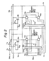
- Figure 2 shows the connection of the power switching circuits 5a and 5b and decoder circuits Ila and Ilb, represented as logic gates.
- the IC memory devices la and Ib include memory cells and control circuits. However, only address converter circuits CNV a and CNV b and decoder circuits IIa and Ilb are shown in Fig. 2.
- the decoder circuit Ila consists of NAND gates Il a , through II an
- the decoder circuit Ilb consists of NAND gates II bl through II bn .
- Each of the NAND gates Il a , through II an and II bl through II bn receives an internal address signal SAi, converted from the external address signal SAe by the address converting circuits CNV a and CNV b , and outputs a word line activation signal corresponding to one of the memory cells of the memory cells MCa and MCb in the memory devices la and lb.
- the power consumption of the decoder circuit of a memory is approximately one-third to one- half of the total power consumption of the memory device.
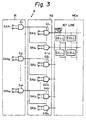
- Figure 3 is a block diagram of a memory device, for example, an IC memory device which s the general arrangement of devices in accordance with the present invention and the prior art.
- the memory device includes a decoder circuit 9 consisting of a first-stage decoder 91 and a second-stage decoder 92, a plurality of semiconductor memory cells MCa storing information, a group of word lines connected to the second-stage decoder 92, and a group of bit lines connected to a multiplexer (not shown).
- the first-stage decoder 91 consists of a plurality of AND gates G l through G m (m is an integer).
- the second- stage decoder 92 consists of a plurality of NAND gate groups GI 1 to Gl n , G2 l to G2 n , ---, Gm l to Gm n (n is an integer), each group being activated by one of the gates of the first-stage decoder 91, as shown in Fig. 3.
- Each set of a first-stage decoder gate and a corresponding group of second-stage decoder gates defines a predetermined range of word lines.
- the gate G 1 corresponds to the power switching circuit 5a in Fig. 2 and the gates-Gl n to Gl n to the decoder circuit Ila in Fig. 2.
- the first-stage decoder 91 consists of a plurality of gates G 1 to G m , c) each of gates G 1 to G m activates a group of gates of the second-stage decoder 92 connected thereto, and d) only one set of a first-stage decoder gate and corresponding second-stage decoder can operate in response to an address signal upon an access command.
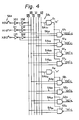
- Figure 4 shows a circuit for converting from the external address signal SAe to the internal address signal SAi connected to the first- and second-stage decoder gates.
- the external address signal SAe consists of three binary bits, i.e., XO representing 2°, XI representing 2 1 , and X2 representing 2 2 .
- the range of the external address signal SAe is 0 to 7, as shown in Table I.
- two series inverters 101 and 102 are provided on the XO bit line, III and ll2 on the XI bit line, and 121 and 122 on the X2 bit line.
- inverted signals XO to X2 and reinverted (non-inverted signals) XO to X2 are generated.
- the higher bits SA hl to SA hm (or bit groups) of the internal address signal are connected to the first-stage decoder 91 so as to operate one of the gates G 1 to Gm .
- the lower bits (or bit groups) SA 21 to SA 2n of the internal address signal are connected to the second- stage decoder 92.
- the internal address signal SAi is connected to each group of gates of the second-stage decoder 92 in the same way. Therefore, for example, the connections of the internal address signal SAi to gates Gl l , G2, ..., Gm n are the same.
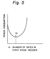
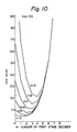
- Figure 5 shows the relationship between the number of gates in the first-stage decoder 91 (horizontal axis) and the power consumption of decoder circuit 9 (vertical axis).
- the curve shows the minimum power consumption is achieved with 10 gates. This will be explained later in detail.
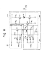
- FIG. 6 is detailed circuit diagram of an example of the first-stage decoder gate G l and the second- stage decoder gate GI 1 shown in Fig. 3.
- the gate G 1 includes a power switching transistor 8, a bias resistor RI, and diodes 7a, and 7 a2 connected in parallel.
- the collector of the transistor 8 is connected to the power line Vcc, and the base is connected to the connection point of anodes of the diodes 7a, and 7 a2 and the resistor RI.
- the emitter of the transistor 8 is connected to the corresponding gate Gl l .
- the gate Gl l comprises an AND gate portion l al and an inverter portion l a2 .
- the AND gate portion l al includes diodes Ilia to IIlc connected in parallel and a bias resistor R B .
- the inverter portion l a2 includes transistors 12 to 14, resistors R3 to R5, and a diode 15.
- the base of the transistor 12 is connected to the connection point of the anodes of the diodes IIIa to IIIc and the resistor R B ; the collector is connected to the power line Vcc through the resistor R3; and the emitter is grounded through the resistor R4.
- the emitter of the transistor 12 is also connected the base of the transistor 14, and the collector is connected to the base of the transistor 13.
- the transistors 13 and 14 are connected in series through the diode 15.
- the collector of the transistor 13 is connected to the power line Vcc through the resistor R5, and the emitter is connected to the anode of the diode 15.
- the collector of the transistor 14 is connected to the cathode of the diode 15, and the emitter is grounded.
- the word-line activation signal SWL is output at the terminal 16 connected to the collector of the transistor 14.
- the higher bits SA hl of the internal address signal in this case two bits, are applied to the cathodes of the diodes 7al and 7a2, and the lower bits SA 2i ; of the internal address signal, in this case three bits, are applied to the cathodes of the diodes Illa to Illc.
- the diodes 7al and 7a2 form an AND gate.
- the diodes IIIa to Illc also form an AND gate.
- the transistor 8 in the gate G 1 is an npn-type transistor instead of the pnp-transistor 8a.
- an npn-type transistor can be produced as a so-called "vertical" type transistor where an n-type epitaxial growth layer is formed on a p-type substrate. Therefore, an npn-type transistor has a high-frequency characteristic and a higher amplification factor compared with a pnp-type transistor, whereby the memory device formed by the npn-type transistor can provide a higher speed decoding operation and a better power switching operation than the prior memory system. Also the production process of an npn-type transistor is simpler than that of a pnp-type transistor.
- one of the lower bits SA ll of the internal address signal applied to the diodes Illa to IIlc is the low level, whereby almost all of the emitter current of the transistor 8 flows to one of the diodes IIIa to Illc.
- the base of the first transistor 12 in the inverter portion l a2 receives the bias voltage and the transistor 12 is turned on.
- a small emitter current of the transistor 12 flows to the ground through the resistor R4. Consequently, the third transistor 14 cannot be turned on, and the output signal SWL at the terminal 16 is the high level, which means non-selection of the word line.
- the transistor 8 in the gate G 1 When the transistor 8 in the gate G 1 is in the off state, the first and third transistors 12 and 14 are also off.
- the gate of the first-stage decoder when the gate of the first-stage decoder is not in operation, the power consumption of the set of the first-stage decoder gate and the corresponding second-- stage decoder gates is almost zero. Only one set of a first-stage decoder gate and corresponding second- stage decoder gates in the memory device is powered upon an access command. In addition, when one set is activated, only the first-stage decoder gate and one of the second-stage decoder gates are powered. The other second-stage decoder gates are not powered. This means a considerable reduction in the power consumption of the decoder circuit.
- a stray capacitance C s may be caused between the anodes of the diodes Illa to IIIc and the ground, i.e., between the base and the ground of the transistor 12, whereby too long a time may be taken after the transistor 8 turns off until the first transistor 12 in the inverter portion l a2 turns off, due to the time constant of the capacitance C s and the resistor R B . If the resistance of the resistor R B is large, the time for discharging the charge stored in the capacitance C s while the transistor 8 is turning on becomes too long.
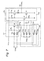
- Figure 7 shows a first embodiment of the present invention in which this situation is improved.
- the circuit shown in Fig. 7 has an additional AND portion l a3 consisting of diodes l7 al and 17 a2 connected in parallel to make an AND gate.
- the cathodes of the diodes 17a, and 17 a2 receive the higher bits of the internal address signal similarly to the cathodes of the diodes 7a, and 7 a2 .
- the anodes are connected together and to the connection point of the anodes of the diodes Illa to IIlc, resistor R B ' and the base of transistor 12.
- the charge stored in the stray capacitance C s formed between the base of the transistor 12 and the ground is discharged through the diodes l7 al and l7 a2 .
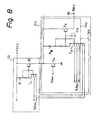
- Figure 8 shows another embodiment of the decoder circuit.
- the operation time of the decoder circuit is improved by using the transistor-transistor -logic (TTL) technology.
- the first-stage decoder gate G 1 comprises a power switching transistor 8 similar to that of Figs. 6 and 7 and a multiemitter transistor T l instead of the diodes 7 al and 7 a2 .
- the higher bits of the internal address signal are applied to the emitters of the transistor T l .
- the second-stage decoder gate Gl l includes transistors T 4 and T 3 , a multiemitter transistor T 2 , and a resistor R B .
- the higher and lower bits of the internal address signal are applied to the emitters of the transistor T 2 as similar to Fig. 7.
- the base of the transistor T4 receives a reference voltage V ref ; the collector is connected to the emitter of transistor 8; and the emitter is grounded.
- the emitter of transistor 8 is also connected to the base of the transistor T 3 and the collector of the multiemitter transistor T 2 through the resistor R B .
- the number (m) of gates of the first-stage decoder 91 for minimizing the current of the second--stage decoder gates GX 1 to GX n (X is an arbitrary number of I to m) will be considered.
- the overall decoder driver-circuit current IDD is defined as follows: where,
- the currents l l to l 5 are determined by the resistance of the resistors in the circuit and do not depend on the numbers m and n.
- the currents I l to 1 5 and N are constant.
- the curve of IDD with a parameter M is basically an upward facing parabola. Accordingly, the minimum value of IDD is given by the following equation:
- the optimum number m of gates of the first-stage decoder can be obtained from equation (6).
- the number m must be an integer, the optimum number of gates of the first-stage decoder is determined as the integer nearest to the value given by equation (6).
- the current consumption of the decoder circuit under the optimum number m can be obtained by equation (I).
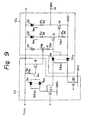
- the actual current of the circuit shown in Fig. 9, which is similar to that of Fig. 7, is calculated as an example.
- reference numerals 20 and 21 represent address inverter transistors for pulling the address signal of the first-stage and second-stage decoders into the ground.
- Reference numerals 22 and 23 are diodes connected between the resistors R 3 and R 5 and the power line Vcc.
- the transistor 8 in Fig. 9 is turned on, whereby the current I RB flows through the resistors R B .
- the transistors 20 and 21 are turned off and the transistor 12 in the gate Gl l is turned on, whereby the current I R3 flows through the resistor R 3 .
- the base of the transistor 14 receives the emitter current of the transistor 12, and the transistor 14 is turned on, whereby the current I R5 flows through the resistor Rs.
- Table 3 represents the calculated currents I RB , I R3 ' and I R5 and the total current I 3 under a power (Vcc) of 4.5V, 5.0V, and 5.5V.
- the transistor 8 shown in Fig. 9 is turned on, the transistor 21 is turned off, and the transistor 20 is turned on. Accordingly, almost all of the current I RB flowing through the resistor R B flows into the ground through the diode Illn, the collector of the transistor 20, and the emitter thereof. Also, the transistor 12 in gate Gl l is turned on, whereby the emitter current I R4 of the transistor 12 flows into the ground through the resistor R 4 .
- Table 4 represents the calculated currents I RB and I R4 and the total current 1 4 under a power (Vcc) of 4.5V, 5.0V, and 5.5V. In this case, the current l l is zero.
- the transistors 8, 12, and 14 are turned off, however, the transistor 20 and 21 re tuned on. Accordingly, the current l Rl flowing through the resistor R, , i.e., the current 1 2 , flows into the round through diode 7an and the collector and emitter of transistor 21.
- Table 5 represents the current l Rl alculated under a power (Vcc) of 4.5V, 5.0V, 5.5V. The ,current l 5 is zero.
- Equation (I) the optimum number m given by the above process is substituted into equation (I).
- Table 6 represents the current consumption IDD of the decoder circuit in accordance with the above condition.
- the current consumption of a prior art decoder circuit is shown in Table 7.
- the current consumption of the prior art decoder circuit is calculated using a circuit similar to that shown in Fig. 9.
- the circuit is constructed as a single chip.
- Figure 10 shows current consumption (IDD) curves depending on the number (m) of gates of the first-stage decoder and the number (n) of gates of the second-stage decoder under a power (Vcc) of 5.0V. From the curves shown in Fig. 10, the optimum combination of m and n can be obtained,
- a decoder circuit of a two-stage construction as in the present invention can significantly reduce the power consumption of the decoder circuit compared with the prior art decoder circuit.
- the decoder circuit in accordance with the present invention when used in a one-chip programmable read only memory device of 64K bits and there are three gates of the first-stage decoder and eight gates of the second-stage decoder, the current consumption is 15 mA.
- the prior art decoder circuit consumes 68 mA under the same conditions.
- a decoder circuit in accordance with the present invention may be constructed with three or more stages in consideration of the power consumption and the complexity of the circuit.
- the present invention provides a semiconductor memory device of considerably reduced power consumption and improved operation time.
- the manufacturing process of the semiconductor memory device including npn transistors becomes simple.
Description
- The present invention relates to a semiconductor memory device, more particularly to a semiconductor memory device of reduced power consumption.
- As is well known, a semiconductor memory device includes a plurality of memory cells arranged in a matrix form, a decoder circuit, a multiplexer circuit, a group of word lines connected to the decoder circuit to activate one of the rows of the matrix, and a group of bit lines connected to the multiplexer circuit to activate one of the columns of the matrix. When a memory system requires a memory capacity over that of a single memory device, two or more memory devices are provided in parallel.
- The conventional technique for reducing power consumption of a memory system is to provide a switching circuit outside each memory device. The switching circuit is connected to the power supply terminal of the memory device. Using the switching circuit, it is possible to supply power only to the memory device which is to be accessed, i.e., power is not supplied to other memory devices.
- This method, however, is disadvantageous in that the switching time for the switching circuit outside of the memory device increases the memory access time.
- Also, this method is rapidly losing its effectiveness in the face of the recent increases in memory capacities of individual memory devices, now 64K bits or 128K bits, and the resultant increases in the size of the memory devices. It is no longer sufficient to reduce the power consumption by switching off power to non-accessed memory circuits.
- EP-A-0024894 describes a semiconductor memory device comprising a plurality of rows of memory cells; and decoder means for selecting one row of the matrix in response to a corresponding one of a plurality of address signals, the decoder means comprising a first stage decoder having a plurality of first stage decoding elements, each of the first stage decoding elements being connected to a plurality of second stage decoding elements of a second stage decoder, wherein each of the first stage decoding elements receives part of the plurality of address signals, whereby one of the second stage decoding elements causes a row of the matrix to be selected, and wherein each of the second stage decoding elements includes at least one second gate circuit receiving said remaining part of the plurality of address signals, the output of the second gate circuit being connected to the output of the respective first stage decoding element, and at least one switching element having a trigger terminal connected to the output of the respective first stage decoding element, the output of the switching element selecting one of the rows of memory cells when the output of the corresponding first stage decoding element is high and the output of the second gate circuit is high.
- US-A-4027285 discloses the use of Schottky barrier diodes in decoder AND gates.
- This device suffers from problems of high power consumption and low speed operation.
- In accordance with one aspect of the present invention, a semiconductor memory device comprises a plurality of rows of memory cells; and decoder means for selecting one row of the matrix in response to a corresponding one of a plurality of address signals, the decoder means comprising a first stage decoder having a plurality of first stage decoding elements, each of the first stage decoding elements being connected to a plurality of second stage decoding elements of a second stage decoder, wherein each of the first stage decoding elements receives part of the plurality of address signals, whereby one of the second stage decoding elements causes a row of the matrix to be selected, and wherein each of the second stage decoding elements includes at least one second gate circuit receiving said remaining part of the plurality of address signals, the output of the second gate circuit being connected to the output of the respective first stage decoding element, and at least one switching element having a trigger terminal connected to the output of the respective first stage decoding element, the output of the switching element selecting one of the rows of memory cells when the output of the corresponding first stage decoding element is high and the output of the second gate circuit is high, and is characterised in that the second gate circuit comprises a plurality of diodes arranged to form an AND gate and in that each second gate circuit includes an extra gate portion comprising a number of diodes arranged to form an AND gate and for receiving the part of the address signals fed to the corresponding first stage decoding elements.
- In accordance with a second aspect of the present invention, a semiconductor memory device comprises a plurality of rows of memory cells; and decoder means for selecting one row of the matrix in response to a corresponding one of a plurality of address signals, the decoder means comprising a first stage decoder having a plurality of first stage decoding elements, each of the first stage decoding elements being connected to a plurality of second stage decoding elements of a second stage decoder, wherein each of the first stage decoding elements receives part of the plurality of address signals, whereby one of the second stage decoding elements causes a row of the matrix to be selected, and wherein each of the second stage decoding elements includes at least one second gate circuit receiving said remaining part of the plurality of address signals, the output of the second gate circuit being connected to the output of the respective first stage decoding element, and at least one switching element having a trigger terminal connected to the output of the respective first stage decoding element, the output of the switching element selecting one of the rows of memory cells when the output of the corresponding first stage decoding element is high and the output of the second gate circuit is high and is characterised in that the second gate circuit comprises a multi-emitter transistor forming an AND gate and to respective emitters of which are fed said remaining part of the plurality of address signals and the part of the address signals fed to the corresponding first stage decoding elements.
- By applying to the second gate circuit or multi-emitter transistor the part of the address signal which is fed to the corresponding first stage decoding element a significant increase in the speed of operation of the device is achieved. The device also has a reduced power consumption over conventional devices.
- Some examples of semiconductor memory devices in accordance with the present invention will now be described and contrasted with a prior art device with reference to the accompanying drawings, in which:
- Figure 1 is a circuit diagram of a prior art memory system including two memory devices arranged in parallel and two external switching circuits connected to the memory devices;
- Figure 2 is a circuit diagram of the external switching circuits and the decoder circuits in the memory devices shown in Figure 1;
- Figure 3 is a block diagram of a memory device showing those elements common to both the invention and the prior art;
- Figure 4 is a circuit diagram of a circuit for converting an external address signal to an internal address signal connected to the decoder circuit of the device shown in Figure 3;
- Figure 5 is a curve showing the general relationship between the number of first-stage decoding gates and the power consumption of the decoder circuit in semiconductor memory devices;
- Figure 6 shows an embodiment of the decoder circuit shown in Figure 3;
- Figure 7 shows a first embodiment of the decoder circuit shown in Figure 3 in accordance with the invention;
- Figure 8 shows still another embodiment of the decoder circuit shown in Figure 3 in accordance with the invention;
- Figure 9 shows another embodiment of the decoder circuit shown in Figure 3,some features of which are applicable to the Figure 7 embodiment; and,
- Figure 10 shows specific curves concerning the curve shown in Figure 4.
- Before describing a preferred embodiment of the present invention, an explanation will be given of the prior art for reference.
- Figure 1 shows a prior art circuit of a memory system including two integrated semiconductor circuit (IC) memory devices provided in parallel. In Figure 1, the IC memory devices la,lb have, for example, 32K bits capacities and are arranged in parallel through the
line 4. This memory system therefore has a 64K bit capacity. When the input terminals at the IC memory devices la and/or Ib receive an external address signal SAe, consisting of Ao through Aj binary signals, the contents stored in the accessed memory cell is output as the read signal SRa and/or SRb. - In order to reduce the power consumption, the memory devices la and Ib are externally provided with
power switching circuits inverter 7a, so as to generate a reversed signal SWb, and is reversed again by aninverter 7b. The switching signals SWb and SWa are applied to the bases of power switchingpnp transistors power switching circuits transistors - Resistors Rla and Rlb are bias resistors.
- Figure 2 shows the connection of the
power switching circuits - Generally, the power consumption of the decoder circuit of a memory is approximately one-third to one- half of the total power consumption of the memory device.
- In the prior art memory system comprising two-stage decoder circuits, i.e., a first stage consisting of the
power switching circuits power switching transistors - Figure 3 is a block diagram of a memory device, for example, an IC memory device which s the general arrangement of devices in accordance with the present invention and the prior art. In Fig. 3, the memory device includes a
decoder circuit 9 consisting of a first-stage decoder 91 and a second-stage decoder 92, a plurality of semiconductor memory cells MCa storing information, a group of word lines connected to the second-stage decoder 92, and a group of bit lines connected to a multiplexer (not shown). The first-stage decoder 91 consists of a plurality of AND gates Gl through Gm (m is an integer). The second-stage decoder 92 consists of a plurality of NAND gate groups GI1 to Gln , G2l to G2n , ---, Gml to Gmn (n is an integer), each group being activated by one of the gates of the first-stage decoder 91, as shown in Fig. 3. - Each set of a first-stage decoder gate and a corresponding group of second-stage decoder gates, for example, the gate G1 and the gates Gll to Gln , defines a predetermined range of word lines.
- In the
decoder circuit 9 shown in Fig. 3, the gate G1 corresponds to thepower switching circuit 5a in Fig. 2 and the gates-Gln to Gln to the decoder circuit Ila in Fig. 2. There are, however, substantial differences between the two constructions, i.e., a) first-stage decoder 91 is built into the memory device, b) the first-stage decoder 91 consists of a plurality of gates G1 to Gm , c) each of gates G1 to Gm activates a group of gates of the second-stage decoder 92 connected thereto, and d) only one set of a first-stage decoder gate and corresponding second-stage decoder can operate in response to an address signal upon an access command. - Figure 4 shows a circuit for converting from the external address signal SAe to the internal address signal SAi connected to the first- and second-stage decoder gates. In this example, the external address signal SAe consists of three binary bits, i.e., XO representing 2°, XI representing 21, and X2 representing 22. The range of the external address signal SAe is 0 to 7, as shown in Table I.

series inverters - In this example, the first-
stage decoder 91 has two (m = 2) gates, and the second-stage decoder 92 has eight ((n = 4) x 2) gates. Therefore, the internal address signal SAi, which can be generated by the combination of any inverted and reinverted signals, is connected to gates Gl and G2 , which are "high (H)" level when they supply power to the corresponding decoder gates, and gates Gl1 to G4 and G2, to G24 , which are "low (L)" level when one of them activates the corresponding word line. - As can be understood from the above in general, the higher bits SAhl to SAhm (or bit groups) of the internal address signal are connected to the first-
stage decoder 91 so as to operate one of the gates G1 to Gm . The lower bits (or bit groups) SA21 to SA2n of the internal address signal are connected to the second-stage decoder 92. The internal address signal SAi is connected to each group of gates of the second-stage decoder 92 in the same way. Therefore, for example, the connections of the internal address signal SAi to gates Gll , G2, ..., Gmn are the same. - In the embodiment shown in Figs. 3 and 4, only one set of a first-stage decoder gate and corresponding second-stage decoder gates, for example, the set of gate Gl and gates Gll to Gln, is operated upon an access command. The other sets are not operated. Therefore, only one set of gates consumes power in the
decoder circuit 9. To obtain the minimum power consumption of thedecoder circuit 9, the optimal division or distribution of the gates of the first--stage decoder 91 and the corresponding gates of the second-stage decoder 92 should be considered. - Figure 5 shows the relationship between the number of gates in the first-stage decoder 91 (horizontal axis) and the power consumption of decoder circuit 9 (vertical axis). The curve shows the minimum power consumption is achieved with 10 gates. This will be explained later in detail.
- Figure 6 is detailed circuit diagram of an example of the first-stage decoder gate Gl and the second- stage decoder gate GI1 shown in Fig. 3. The gate G1 includes a
power switching transistor 8, a bias resistor RI, anddiodes transistor 8 is connected to the power line Vcc, and the base is connected to the connection point of anodes of thediodes transistor 8 is connected to the corresponding gate Gll. - In this embodiment, the gate Gll comprises an AND gate portion lal and an inverter portion la2. The AND gate portion lal includes diodes Ilia to IIlc connected in parallel and a bias resistor RB. The inverter portion la2 includes
transistors 12 to 14, resistors R3 to R5, and adiode 15. The base of thetransistor 12 is connected to the connection point of the anodes of the diodes IIIa to IIIc and the resistor RB; the collector is connected to the power line Vcc through the resistor R3; and the emitter is grounded through the resistor R4. The emitter of thetransistor 12 is also connected the base of thetransistor 14, and the collector is connected to the base of thetransistor 13. Thetransistors diode 15. The collector of thetransistor 13 is connected to the power line Vcc through the resistor R5, and the emitter is connected to the anode of thediode 15. The collector of thetransistor 14 is connected to the cathode of thediode 15, and the emitter is grounded. - The word-line activation signal SWL is output at the terminal 16 connected to the collector of the
transistor 14. - In this embodiment, the higher bits SAhl of the internal address signal, in this case two bits, are applied to the cathodes of the diodes 7al and 7a2, and the lower bits SA2i; of the internal address signal, in this case three bits, are applied to the cathodes of the diodes Illa to Illc. The diodes 7al and 7a2 form an AND gate. The diodes IIIa to Illc also form an AND gate.
- Comparing the gate Gl in Fig. 6 with the
power switching circuit 5a in Fig. I, thetransistor 8 in the gate G1 is an npn-type transistor instead of the pnp-transistor 8a. There is the distinctive merit that an npn-type transistor can be produced as a so-called "vertical" type transistor where an n-type epitaxial growth layer is formed on a p-type substrate. Therefore, an npn-type transistor has a high-frequency characteristic and a higher amplification factor compared with a pnp-type transistor, whereby the memory device formed by the npn-type transistor can provide a higher speed decoding operation and a better power switching operation than the prior memory system. Also the production process of an npn-type transistor is simpler than that of a pnp-type transistor. - The above-mentioned merits also apply to the npn-
type transistors 12 to 14 in the gate Gll shown in Fig. 6. - The operation of the circuit shown in Fig. 6 will be described below. When all of the higher bits SAhl of the internal address signal applied to the cathodes of the
diodes npn transistor 8 is turned on. In addition, when all of the lower bits SA21, of the internal address signal applied to the cathodes of the diodes Illa to IIlc provided in the AND gate portion lal are the high level, thetransistors - When the
transistor 8 is kept in the on state, however, one of the lower bits SAℓl of the internal address signal applied to the diodes Illa to IIlc is the low level, whereby almost all of the emitter current of thetransistor 8 flows to one of the diodes IIIa to Illc. The base of thefirst transistor 12 in the inverter portion la2 receives the bias voltage and thetransistor 12 is turned on. However, a small emitter current of thetransistor 12 flows to the ground through the resistor R4. Consequently, thethird transistor 14 cannot be turned on, and the output signal SWL at the terminal 16 is the high level, which means non-selection of the word line. - When the
transistor 8 in the gate G1 is in the off state, the first andthird transistors - As can be understood from the above explanation, when the gate of the first-stage decoder is not in operation, the power consumption of the set of the first-stage decoder gate and the corresponding second-- stage decoder gates is almost zero. Only one set of a first-stage decoder gate and corresponding second- stage decoder gates in the memory device is powered upon an access command. In addition, when one set is activated, only the first-stage decoder gate and one of the second-stage decoder gates are powered. The other second-stage decoder gates are not powered. This means a considerable reduction in the power consumption of the decoder circuit.
- In the circuit in Fig. 6, use of Schottky barrier diodes for the
diodes - The above AND circuits consisting of the
diodes - Now, in the circuit in Fig. 6, the higher bits of the internal address signal applied to the
diodes transistor 12, whereby too long a time may be taken after thetransistor 8 turns off until thefirst transistor 12 in the inverter portion la2 turns off, due to the time constant of the capacitance Cs and the resistor RB. If the resistance of the resistor RB is large, the time for discharging the charge stored in the capacitance Cs while thetransistor 8 is turning on becomes too long. - Figure 7 shows a first embodiment of the present invention in which this situation is improved. The circuit shown in Fig. 7 has an additional AND portion la3 consisting of diodes l7al and 17a2 connected in parallel to make an AND gate. The cathodes of the diodes 17a, and 17a2 receive the higher bits of the internal address signal similarly to the cathodes of the
diodes transistor 12. - In accordance with the circuit shown in Fig. 7, the charge stored in the stray capacitance Cs formed between the base of the
transistor 12 and the ground is discharged through the diodes l7al and l7a2. - Figure 8 shows another embodiment of the decoder circuit. In this circuit, the operation time of the decoder circuit is improved by using the transistor-transistor -logic (TTL) technology. The first-stage decoder gate G1 comprises a
power switching transistor 8 similar to that of Figs. 6 and 7 and a multiemitter transistor Tl instead of thediodes transistor 8; and the emitter is grounded. The emitter oftransistor 8 is also connected to the base of the transistor T3 and the collector of the multiemitter transistor T2 through the resistor RB. - The basic principle of operation of this circuit is similar to that of the circuit shown in Fig. 7. Accordingly, the explanation of this circuit operation is omitted.
- Determination of the number of gates of the first--stage and second-stage decoders for the minimum power consumption of the decoder circuit will be explained below with reference to the circuit shown in Fig. 3.
- First, the number (m) of gates of the first-
stage decoder 91 for minimizing the current of the second-- stage decoder gates GX1 to GXn (X is an arbitrary number of I to m) will be considered. - The overall decoder driver-circuit current IDD is defined as follows:

- m: number of gates of the first-stage decoder,
- n: number of gates of the second-stage decoder,
- Il: current flowing in the selected gate of first-stage decoder and not supplied to the gates of the
- second-stage decoder (only the current consumed by the gate of the first--stage decoder and not that supplied from the gate of the first-stage decoder to be gates of the second-stage decoder),
- 12: current flowing in the non-selected gates of the first-stage decoder,
- 13: current flowing in the selected gates of the second-stage decoder,
- 14: current flowing in the non-selected gates of the secondstage decoder connected to the selected gate of the first-stage decoder, and
- I5: current flowing in the non-selected gates of the first-stage decoder.
- The currents ll to l5 are determined by the resistance of the resistors in the circuit and do not depend on the numbers m and n.
- Rewriting the
notations 2" and 2m as N and M equation (I), one obtains:
- Rewriting the above equation, one obtains:

- The currents Il to 15 and N are constant.
- Differentiating equation (2) by m, one obtains:

- Further differentiating equation (3) by M, one obtains:

- As 14 » 15 , the curve of IDD with a parameter M is basically an upward facing parabola. Accordingly, the minimum value of IDD is given by the following equation:

- From equations (3) and (5), the following equation is derived:

- Rewriting this to the original form, one obtains:

- The optimum number m of gates of the first-stage decoder can be obtained from equation (6). As the number m must be an integer, the optimum number of gates of the first-stage decoder is determined as the integer nearest to the value given by equation (6).
- The current consumption of the decoder circuit under the optimum number m can be obtained by equation (I). The actual current of the circuit shown in Fig. 9, which is similar to that of Fig. 7, is calculated as an example. In Fig. 9,
reference numerals 20 and 21 represent address inverter transistors for pulling the address signal of the first-stage and second-stage decoders into the ground.Reference numerals - In this example, the currents IR, , IRB , IR3 , IR4 , and IR5 flowing through the resistors Rl , RB , R3 , R4 , and R5 are calculated, assuming the resistances DRl = R3 = R4 = R5 = 5 kΩ and RB = 15 kΩ.
- The possible combinations of selection of the gates of the first-stage and second-stage decoders are shown in Table 2.

- In case I of Table 2, the
transistor 8 in Fig. 9 is turned on, whereby the current IRB flows through the resistors RB. At this time, thetransistors 20 and 21 are turned off and thetransistor 12 in the gate Gll is turned on, whereby the current IR3 flows through the resistor R3. Also, the base of thetransistor 14 receives the emitter current of thetransistor 12, and thetransistor 14 is turned on, whereby the current IR5 flows through the resistor Rs. Table 3 represents the calculated currents IRB , IR3 ' and IR5 and the total current I3 under a power (Vcc) of 4.5V, 5.0V, and 5.5V.
- Next, in
case 2 of Table 2, thetransistor 8 shown in Fig. 9 is turned on, the transistor 21 is turned off, and thetransistor 20 is turned on. Accordingly, almost all of the current IRB flowing through the resistor RB flows into the ground through the diode Illn, the collector of thetransistor 20, and the emitter thereof. Also, thetransistor 12 in gate Gll is turned on, whereby the emitter current IR4 of thetransistor 12 flows into the ground through the resistor R4. Table 4 represents the calculated currents IRB and IR4 and the total current 14 under a power (Vcc) of 4.5V, 5.0V, and 5.5V. In this case, the current ll is zero.
- Finally, in
case 3 of Table 2, thetransistors transistor 20 and 21 re tuned on. Accordingly, the current lRl flowing through the resistor R, , i.e., the current 12 , flows into the round through diode 7an and the collector and emitter of transistor 21. Table 5 represents the current lRl alculated under a power (Vcc) of 4.5V, 5.0V, 5.5V. The ,current l5 is zero.
- In order to obtain the opitimum number m of gates of the first-stage decoder for the number n of gates of the second-stage decoder, the currents ll to 15 given in Table 3 to 5 are substituted into equation (5).
- In order to obtain the minimum current consumption IDD of the decoder circuit, the optimum number m given by the above process is substituted into equation (I). Table 6 represents the current consumption IDD of the decoder circuit in accordance with the above condition.

- By way of reference in evaluating the present invention, the current consumption of a prior art decoder circuit is shown in Table 7. The current consumption of the prior art decoder circuit is calculated using a circuit similar to that shown in Fig. 9. The circuit is constructed as a single chip.

- Figure 10 shows current consumption (IDD) curves depending on the number (m) of gates of the first-stage decoder and the number (n) of gates of the second-stage decoder under a power (Vcc) of 5.0V. From the curves shown in Fig. 10, the optimum combination of m and n can be obtained,
- As can be clearly understood from Tables 6 and 7, a decoder circuit of a two-stage construction as in the present invention can significantly reduce the power consumption of the decoder circuit compared with the prior art decoder circuit.
- For example, when the decoder circuit in accordance with the present invention is used in a one-chip programmable read only memory device of 64K bits and there are three gates of the first-stage decoder and eight gates of the second-stage decoder, the current consumption is 15 mA. On the other hand, the prior art decoder circuit consumes 68 mA under the same conditions.
- While the above embodiments were described with reference to the memory system shown in Figs. I and 2, the essence of the present invention is to form a two-stage decoder circuit. The external switching circuits shown in Figures 1 and 2 can also be applied to a memory system including a plurality of memory devices in accordance with the present invention.
- In addition, a decoder circuit in accordance with the present invention may be constructed with three or more stages in consideration of the power consumption and the complexity of the circuit.
- Thus the present invention provides a semiconductor memory device of considerably reduced power consumption and improved operation time. In addition, the manufacturing process of the semiconductor memory device including npn transistors becomes simple.
Claims (6)
Applications Claiming Priority (2)
| Application Number | Priority Date | Filing Date | Title |
|---|---|---|---|
| JP57233906A JPS59124092A (en) | 1982-12-29 | 1982-12-29 | Memory device |
| JP233906/82 | 1982-12-29 |
Publications (3)
| Publication Number | Publication Date |
|---|---|
| EP0115187A2 EP0115187A2 (en) | 1984-08-08 |
| EP0115187A3 EP0115187A3 (en) | 1986-12-30 |
| EP0115187B1 true EP0115187B1 (en) | 1991-02-20 |
Family
ID=16962433
Family Applications (1)
| Application Number | Title | Priority Date | Filing Date |
|---|---|---|---|
| EP83307901A Expired - Lifetime EP0115187B1 (en) | 1982-12-29 | 1983-12-22 | Semiconductor memory device with decoder means |
Country Status (5)
| Country | Link |
|---|---|
| US (1) | US4617653A (en) |
| EP (1) | EP0115187B1 (en) |
| JP (1) | JPS59124092A (en) |
| DE (1) | DE3382163D1 (en) |
| IE (1) | IE56715B1 (en) |
Families Citing this family (15)
| Publication number | Priority date | Publication date | Assignee | Title |
|---|---|---|---|---|
| JPS6148192A (en) * | 1984-08-11 | 1986-03-08 | Fujitsu Ltd | Semiconductor memory device |
| JPS6167154A (en) * | 1984-09-11 | 1986-04-07 | Fujitsu Ltd | Semiconductor storage device |
| JPS61199297A (en) * | 1985-02-28 | 1986-09-03 | Toshiba Corp | Semiconductor memory device |
| JPS61265794A (en) * | 1985-05-20 | 1986-11-25 | Fujitsu Ltd | Decoder circuit of semiconductor storage device |
| JP2603205B2 (en) * | 1987-03-16 | 1997-04-23 | シーメンス、アクチエンゲゼルシヤフト | Multi-stage integrated decoder device |
| US5257234A (en) * | 1987-07-15 | 1993-10-26 | Hitachi, Ltd. | Semiconductor integrated circuit device |
| DE3884492T2 (en) * | 1987-07-15 | 1994-02-17 | Hitachi Ltd | Integrated semiconductor circuit arrangement. |
| KR930001738B1 (en) * | 1989-12-29 | 1993-03-12 | 삼성전자주식회사 | Word-line driver array method of semiconductor memory device |
| KR920010344B1 (en) * | 1989-12-29 | 1992-11-27 | 삼성전자주식회사 | Memory array composition method |
| KR930001737B1 (en) * | 1989-12-29 | 1993-03-12 | 삼성전자 주식회사 | Wordline array method of semiconductor memory device |
| US5652723A (en) * | 1991-04-18 | 1997-07-29 | Mitsubishi Denki Kabushiki Kaisha | Semiconductor memory device |
| EP0596198B1 (en) * | 1992-07-10 | 2000-03-29 | Sony Corporation | Flash eprom with erase verification and address scrambling architecture |
| JP2001126475A (en) * | 1999-10-25 | 2001-05-11 | Mitsubishi Electric Corp | Semiconductor memory |
| US8755213B2 (en) | 2012-02-29 | 2014-06-17 | International Business Machines Corporation | Decoding scheme for bipolar-based diode three-dimensional memory requiring bipolar programming |
| US8842491B2 (en) | 2012-07-17 | 2014-09-23 | International Business Machines Corporation | Decoding scheme for bipolar-based diode three-dimensional memory requiring unipolar programming |
Family Cites Families (7)
| Publication number | Priority date | Publication date | Assignee | Title |
|---|---|---|---|---|
| US3599182A (en) * | 1969-01-15 | 1971-08-10 | Ibm | Means for reducing power consumption in a memory device |
| US3688280A (en) * | 1970-09-22 | 1972-08-29 | Ibm | Monolithic memory system with bi-level powering for reduced power consumption |
| US4027285A (en) * | 1973-12-26 | 1977-05-31 | Motorola, Inc. | Decode circuitry for bipolar random access memory |
| JPS528739A (en) * | 1975-07-10 | 1977-01-22 | Fujitsu Ltd | Electronic circuit |
| JPS5631137A (en) * | 1979-08-22 | 1981-03-28 | Fujitsu Ltd | Decoder circuit |
| JPS56112122A (en) * | 1980-02-08 | 1981-09-04 | Fujitsu Ltd | Decoder circuit |
| JPS5841597B2 (en) * | 1980-12-24 | 1983-09-13 | 富士通株式会社 | Semiconductor memory discharge circuit |
-
1982
- 1982-12-29 JP JP57233906A patent/JPS59124092A/en active Granted
-
1983
- 1983-12-22 DE DE8383307901T patent/DE3382163D1/en not_active Expired - Fee Related
- 1983-12-22 EP EP83307901A patent/EP0115187B1/en not_active Expired - Lifetime
- 1983-12-28 US US06/566,323 patent/US4617653A/en not_active Expired - Fee Related
- 1983-12-29 IE IE3081/83A patent/IE56715B1/en not_active IP Right Cessation
Non-Patent Citations (1)
| Title |
|---|
| C.RINT:"Handbuch für Hochfrequenz-und Elektrotechniker", Volum 3, 1979, München/Heidelberg, Verl.Hüthig und Pflaum, 1979 * |
Also Published As
| Publication number | Publication date |
|---|---|
| JPH0323995B2 (en) | 1991-04-02 |
| EP0115187A2 (en) | 1984-08-08 |
| EP0115187A3 (en) | 1986-12-30 |
| IE833081L (en) | 1984-06-29 |
| DE3382163D1 (en) | 1991-03-28 |
| US4617653A (en) | 1986-10-14 |
| IE56715B1 (en) | 1991-11-20 |
| JPS59124092A (en) | 1984-07-18 |
Similar Documents
| Publication | Publication Date | Title |
|---|---|---|
| EP0115187B1 (en) | Semiconductor memory device with decoder means | |
| US4369503A (en) | Decoder circuit | |
| US5021688A (en) | Two stage address decoder circuit for semiconductor memories | |
| US4745582A (en) | Bipolar-transistor type random access memory device having redundancy configuration | |
| US4385370A (en) | Decoder circuit | |
| US4347585A (en) | Reproduce only storage matrix | |
| US4792923A (en) | Bipolar semiconductor memory device with double word lines structure | |
| EP0503524B1 (en) | Semiconductor memory device | |
| EP0202892B1 (en) | Semiconductor memory device with diode matrix decoder and redundancy configuration | |
| US4586169A (en) | Semiconductor memory circuit and large scale integrated circuit using the same | |
| US4031413A (en) | Memory circuit | |
| US4897820A (en) | Bi-CMOS type of semiconductor memory device | |
| EP0203422A2 (en) | Improved three state select circuit for use in a data processing system | |
| EP0289893B1 (en) | Bipmos decoder circuit | |
| EP0090186A2 (en) | Complementary logic circuit | |
| EP0054853A2 (en) | Semiconductor memory device | |
| JPH0310197B2 (en) | ||
| KR860001322B1 (en) | Non-dissipative memory system | |
| EP0488672B1 (en) | Memory device with current mirror type sense amplifiers | |
| US4791382A (en) | Driver circuit | |
| US5117391A (en) | Bipolar memory cell array biasing technique with forward active PNP load cell | |
| US4697104A (en) | Two stage decoder circuit using threshold logic to decode high-order bits and diode-matrix logic to decode low-order bits | |
| US4899311A (en) | Clamping sense amplifier for bipolar ram | |
| US4613774A (en) | Unitary multiplexer-decoder circuit | |
| US5444654A (en) | ROM with Bi-CMOS gate arrays |
Legal Events
| Date | Code | Title | Description |
|---|---|---|---|
| PUAI | Public reference made under article 153(3) epc to a published international application that has entered the european phase |
Free format text: ORIGINAL CODE: 0009012 |
|
| AK | Designated contracting states |
Designated state(s): DE FR GB |
|
| PUAL | Search report despatched |
Free format text: ORIGINAL CODE: 0009013 |
|
| AK | Designated contracting states |
Kind code of ref document: A3 Designated state(s): DE FR GB |
|
| 17P | Request for examination filed |
Effective date: 19870320 |
|
| 17Q | First examination report despatched |
Effective date: 19880218 |
|
| GRAA | (expected) grant |
Free format text: ORIGINAL CODE: 0009210 |
|
| AK | Designated contracting states |
Kind code of ref document: B1 Designated state(s): DE FR GB |
|
| REF | Corresponds to: |
Ref document number: 3382163 Country of ref document: DE Date of ref document: 19910328 |
|
| ET | Fr: translation filed | ||
| PLBE | No opposition filed within time limit |
Free format text: ORIGINAL CODE: 0009261 |
|
| STAA | Information on the status of an ep patent application or granted ep patent |
Free format text: STATUS: NO OPPOSITION FILED WITHIN TIME LIMIT |
|
| 26N | No opposition filed | ||
| PGFP | Annual fee paid to national office [announced via postgrant information from national office to epo] |
Ref country code: FR Payment date: 19951212 Year of fee payment: 13 |
|
| PGFP | Annual fee paid to national office [announced via postgrant information from national office to epo] |
Ref country code: GB Payment date: 19951213 Year of fee payment: 13 |
|
| PGFP | Annual fee paid to national office [announced via postgrant information from national office to epo] |
Ref country code: DE Payment date: 19951222 Year of fee payment: 13 |
|
| PG25 | Lapsed in a contracting state [announced via postgrant information from national office to epo] |
Ref country code: GB Effective date: 19961222 |
|
| GBPC | Gb: european patent ceased through non-payment of renewal fee |
Effective date: 19961222 |
|
| PG25 | Lapsed in a contracting state [announced via postgrant information from national office to epo] |
Ref country code: FR Effective date: 19970829 |
|
| PG25 | Lapsed in a contracting state [announced via postgrant information from national office to epo] |
Ref country code: DE Effective date: 19970902 |
|
| REG | Reference to a national code |
Ref country code: FR Ref legal event code: ST |