EP0114763A2 - Redundant rows in integrated circuit memories - Google Patents
Redundant rows in integrated circuit memories Download PDFInfo
- Publication number
- EP0114763A2 EP0114763A2 EP84400068A EP84400068A EP0114763A2 EP 0114763 A2 EP0114763 A2 EP 0114763A2 EP 84400068 A EP84400068 A EP 84400068A EP 84400068 A EP84400068 A EP 84400068A EP 0114763 A2 EP0114763 A2 EP 0114763A2
- Authority
- EP
- European Patent Office
- Prior art keywords
- row
- address
- redundant
- rows
- signal
- Prior art date
- Legal status (The legal status is an assumption and is not a legal conclusion. Google has not performed a legal analysis and makes no representation as to the accuracy of the status listed.)
- Withdrawn
Links
Images
Classifications
-
- G—PHYSICS
- G11—INFORMATION STORAGE
- G11C—STATIC STORES
- G11C29/00—Checking stores for correct operation ; Subsequent repair; Testing stores during standby or offline operation
- G11C29/70—Masking faults in memories by using spares or by reconfiguring
- G11C29/78—Masking faults in memories by using spares or by reconfiguring using programmable devices
- G11C29/781—Masking faults in memories by using spares or by reconfiguring using programmable devices combined in a redundant decoder
Definitions
- This invention relates to integrated circuit memories, and in particular, to an apparatus for providing redundant rows in such memories when other portions of the memory are found defective.
- One feature of the present invention is directed to a decoding apparatus for an integrated circuit memory having first rows of memory cells and at least one selectively connectable redundant second row of memory cells for being connected in place of one of the first rows, the apparatus characterized by: redundant decoder means connected to each of the at least one second row, said redundant decoder means including a plurality of selectable connections for creating an address for each of the at least one second row; logic means for generating a control signal of a first stace until an address is supplied to the memory and of a second state if any of the at least one second row is selected by the address; and decoder means connected to receive the control signal from the logic means for controlling the first rows in response thereto.
- the potential of line 10 is also controlled by a smaller decoder connected to receive addresses A4 and A 5 , and control signal ⁇ C . These signals are supplied to transistors 21, 22, and 23 respectively, and thereby control transistors 24 and 26. Of-course, if transistor 26 is on, then line 10 will be pulled to .ground, because transistor 24 will be off.
- the .control signal ⁇ C supplied to transistor 23 is generated using the apparatus shown in Figure 3, and will be discussed in conjunction with that Figure.
- FIG. 2 illustrates the decoding apparatus associated with the redundant row.
- a chip enable signal CE is supplied to transistor 30 to connect the redundant row associated with line 31 to potential V CC unless one of the decoding transistors 32, 33,...n is turned on to pull line 31 to ground.
- Each of these decoding transistors is serially connected with a fuse F 1 , F 2 ,...F n , which, in the preferred embodiment, may be "blown" using a laser. Fuses such as these are well-known in the semiconductor arts. If any of these fuses are blown, then the address signals supplied to the gate of the corresponding transistor will have no effect upon the addressing of row 31. If none of the fuses are blown, then when any address is supplied, the redundant row coupled to line 31 will be pulled to ground, and the presence of the redundant row will not affect the remainder of the memory.
- Figure 3 illustrates the manner in which the control ⁇ C is generated for application to transistor .23.
- a plurality of redundant row addresses RR 1 , RR 2 ...RR n (whose origins are as shown in Figure 2) are applied to an OR gate 35.
- Address inputs A 4 and A 4 are applied to the terminals of exclusive OR gate 46.
- the output signals from gates 45 .and 46 . are supplied to input terminals of NAND gate 47 to thereby generate a control signal ⁇ C , which after being inverted, is used to control transistor 23.
Abstract
Description
- This invention relates to integrated circuit memories, and in particular, to an apparatus for providing redundant rows in such memories when other portions of the memory are found defective.
- In integrated circuit memories, a single defect in any portion of the array of memory cells may render the entire memory useless. As improvements in the-design and fabrication of .integrated circuits are made, greater numbers of memory cells are being placed on a single chip. Furthermore, generally physically larger integrated circuits are being manufactured. Each factor tends to increase the likelihood of a defect in one or-more cells which may,render an entire chip useless.
- One prior art solution to this problem has been to design and fabricate integrated circuit memories using more fault tolerant-designs and processes. This .approach, by itself, does not always suffice. Consequently, another solution which has received increasing attention is the fabrication of redundant components on the same chip. At a suitable stage in the fabrication process, the non-functional portions of the circuit are replaced with the redundant portions, typically by using redundant wiring techniques, fuses, discretionary metal masks, or other techniques. The usual prior art approach, however, has been to replace an entire relatively large block in the memory with a new block. For example, in a 64k memory divided into 16 sections, each of 4k bits, a defective bit in a single section will result in the replacement of the entire 4k section. Unfortunately, this approach requires a considerable amount of extra logic and extra space on the integrated circuit.
- While redundant rows improve yield, and are relatively simple to implement, the addressing scheme for redundant ruws is critical because it lies along the critical signal path. The added decoding circuits for the redundant rows, when selected by laser fusing or other techniques, must select the redundant row and at the same time de-select all the other redundant rows and normal rows of memory cells. At the same time, the operating speed of the overall memory must not be affected by the added circuitry.
- One feature of the present invention is directed to a decoding apparatus for an integrated circuit memory having first rows of memory cells and at least one selectively connectable redundant second row of memory cells for being connected in place of one of the first rows, the apparatus characterized by: redundant decoder means connected to each of the at least one second row, said redundant decoder means including a plurality of selectable connections for creating an address for each of the at least one second row; logic means for generating a control signal of a first stace until an address is supplied to the memory and of a second state if any of the at least one second row is selected by the address; and decoder means connected to receive the control signal from the logic means for controlling the first rows in response thereto.
-
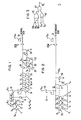
- Figure 1 is an electrical schematic illustrating an addressing circuit for a normal row of an integrated circuit memory.
- Figure 2 is a circuit schematic of a decoder for a redundant row of a memory.
- Figure 3 is a schematic of the circuit used to generate the control signal supplied to Figures 1 and 2.
- Figure 1 is a circuit schematic illustrating typical decoding apparatus for a normal row of memory cells connected to
line 10. The apparatus includestransistors 11, 12, and 13 to which address signals A8, 'A9, and A10 are supplied. The combined signals of these three transistors are applied to the gate oftransistor 14 to selectively connectline 10 to potential VCC, assuming certain other transistors are on. The address signals fromtransistors 11, 12, and 13 are also supplied, after being inverted by inverter 15, to the gate oftransistor 16. As also shown address signal A6 controls transistor 17, address signal A7 controls transistor 18, address A11 controls transistor 19, and address signal A12 controls transistor 20. In a similar fashion address A4 controls transistor 21, address A5 transistor 22, and a control signal.φ C transistor 23. The combined address signals oftransistors control transistor 24 as shown. The same combined address signals inverted byinverter 25 alsocontrol transistor 26. - In operation if the row connected to
line 10 is to be addressed, address signal A8 + A9 + A10 will be low turning ontransistor 14 and pullingrow line 10 to potential VCC during reading of the memory cells attached toline 10. Alternatively,line 10 may be pulled to potential vPP during programming by application of a signal to the node designated PGM. In addition, to addressrow 10transistors line 10 will be pulled to ground. The signal supplied totransistor 16 is complementary to that supplied totransistor 14. - The potential of
line 10 is also controlled by a smaller decoder connected to receive addresses A4 and A5, and control signalφ C. These signals are supplied totransistors transistors transistor 26 is on, thenline 10 will be pulled to .ground, becausetransistor 24 will be off. The .control signalφ C supplied totransistor 23 is generated using the apparatus shown in Figure 3, and will be discussed in conjunction with that Figure. - Figure 2 illustrates the decoding apparatus associated with the redundant row. A chip enable signal CE is supplied to
transistor 30 to connect the redundant row associated withline 31 to potential VCC unless one of thedecoding transistors 32, 33,...n is turned on to pullline 31 to ground. Each of these decoding transistors is serially connected with a fuse F1, F2,...Fn, which, in the preferred embodiment, may be "blown" using a laser. Fuses such as these are well-known in the semiconductor arts. If any of these fuses are blown, then the address signals supplied to the gate of the corresponding transistor will have no effect upon the addressing ofrow 31. If none of the fuses are blown, then when any address is supplied, the redundant row coupled toline 31 will be pulled to ground, and the presence of the redundant row will not affect the remainder of the memory. - If the redundant row is desired, then all fuses are blown except for those corresponding to the desired address of the redundant row. In this manner the redundant row will be pulled to ground only when one or more of its address bits having intact fuses are high. If all the connected address bits are low, then
redundant row 31 will be selected. - Figure 3 illustrates the manner in which the control
φ C is generated for application to transistor .23. As shown in Figure 3, a plurality of redundant row addresses RR1, RR2...RRn, (whose origins are as shown in Figure 2) are applied to an OR gate 35. Address inputs A4 andA4 are applied to the terminals of exclusive ORgate 46. The output signals fromgates 45 .and 46 .are supplied to input terminals ofNAND gate 47 to thereby generate a control signal φC, which after being inverted, is used to controltransistor 23. - For the circuit shown in figures 1,2,and 3 when the chip containing the memory cells is enabled, signal
φ C stays low. All rows, including-any redundant rows., are pulled high,because all addresses are low unconditionally when the chip is deselected until the outputs of the address buffers are valid. Once address signals A4 and A4 are valid, exclusive ORgate 46 supplies a signal to NANDgate 47. If a redundant row has been selected, ORgate 45 will also supply a signal and φC will go low andφ C high to deselect all normal rows. Thus for every redundant row only the selected fuses need be blown to provide the necessary address signals. If no fuses are blown, then the redundant row will not be selected by any address. - Although one embodiment of this invention has been described above, this embodiment is intended to illustrate the invention, rather than limit it. The scope of the invention may be determined from the following claims.
Claims (13)
Applications Claiming Priority (2)
| Application Number | Priority Date | Filing Date | Title |
|---|---|---|---|
| US06/457,999 US4538247A (en) | 1983-01-14 | 1983-01-14 | Redundant rows in integrated circuit memories |
| US457999 | 1990-01-10 |
Publications (2)
| Publication Number | Publication Date |
|---|---|
| EP0114763A2 true EP0114763A2 (en) | 1984-08-01 |
| EP0114763A3 EP0114763A3 (en) | 1988-07-27 |
Family
ID=23818943
Family Applications (1)
| Application Number | Title | Priority Date | Filing Date |
|---|---|---|---|
| EP84400068A Withdrawn EP0114763A3 (en) | 1983-01-14 | 1984-01-13 | Redundant rows in integrated circuit memories |
Country Status (4)
| Country | Link |
|---|---|
| US (1) | US4538247A (en) |
| EP (1) | EP0114763A3 (en) |
| JP (1) | JPS59140700A (en) |
| CA (1) | CA1215471A (en) |
Cited By (5)
| Publication number | Priority date | Publication date | Assignee | Title |
|---|---|---|---|---|
| DE3508157A1 (en) * | 1984-03-08 | 1985-09-19 | Sharp K.K., Osaka | Redundancy circuit for a semiconductor memory |
| FR2598549A1 (en) * | 1986-05-07 | 1987-11-13 | Samsung Semiconductor Tele | Redundancy circuit for use in a semiconductor memory device |
| EP0469252A1 (en) * | 1990-06-19 | 1992-02-05 | Texas Instruments Incorporated | Laser link decoder for DRAM redundancy scheme |
| EP0626644A1 (en) * | 1993-05-28 | 1994-11-30 | STMicroelectronics, Inc. | Structure to utilize a partially functional cache memory |
| EP0675436A1 (en) * | 1994-03-31 | 1995-10-04 | STMicroelectronics, Inc. | Recoverable set associative cache |
Families Citing this family (15)
| Publication number | Priority date | Publication date | Assignee | Title |
|---|---|---|---|---|
| JPS60130000A (en) * | 1983-12-15 | 1985-07-11 | Mitsubishi Electric Corp | Semiconductor storage device |
| US4618784A (en) * | 1985-01-28 | 1986-10-21 | International Business Machines Corporation | High-performance, high-density CMOS decoder/driver circuit |
| US4758744A (en) * | 1986-11-26 | 1988-07-19 | Rca Corporation | Decoder circuitry with reduced number of inverters and bus lines |
| EP0327861B1 (en) * | 1988-02-10 | 1993-03-31 | Siemens Aktiengesellschaft | Redundancy decoder for an integrated semiconductor memory |
| DE3934303C2 (en) * | 1988-10-15 | 2001-01-25 | Sony Corp | Address decoder for non-volatile memories |
| JP2575919B2 (en) * | 1990-03-22 | 1997-01-29 | 株式会社東芝 | Redundancy circuit of semiconductor memory device |
| US5257228A (en) * | 1991-05-16 | 1993-10-26 | Texas Instruments Incorporated | Efficiency improved DRAM row redundancy circuit |
| KR100248165B1 (en) * | 1992-04-16 | 2000-03-15 | 칼 하인쯔 호르닝어 | Integrated semiconductor memory with redundancy arrangement |
| GB9223226D0 (en) * | 1992-11-05 | 1992-12-16 | Algotronix Ltd | Improved configurable cellular array (cal ii) |
| US5369314A (en) * | 1994-02-22 | 1994-11-29 | Altera Corporation | Programmable logic device with redundant circuitry |
| US6091258A (en) * | 1997-02-05 | 2000-07-18 | Altera Corporation | Redundancy circuitry for logic circuits |
| US6034536A (en) * | 1997-02-05 | 2000-03-07 | Altera Corporation | Redundancy circuitry for logic circuits |
| JP3865789B2 (en) * | 1997-05-23 | 2007-01-10 | アルテラ コーポレイション | Redundant circuit for programmable logic device with interleaved input circuit |
| US6201404B1 (en) | 1998-07-14 | 2001-03-13 | Altera Corporation | Programmable logic device with redundant circuitry |
| JP2002064145A (en) * | 2000-06-09 | 2002-02-28 | Fujitsu Ltd | Integrated circuit chip having redundancy element, multiprocessor and method of manufacturing the same |
Family Cites Families (4)
| Publication number | Priority date | Publication date | Assignee | Title |
|---|---|---|---|---|
| US4250570B1 (en) * | 1976-07-15 | 1996-01-02 | Intel Corp | Redundant memory circuit |
| US4059231A (en) * | 1976-07-16 | 1977-11-22 | Grefco, Inc. | Method and apparatus for selectively comminuting particles of a frangible material |
| JPS56174200U (en) * | 1980-05-27 | 1981-12-22 | ||
| US4358833A (en) * | 1980-09-30 | 1982-11-09 | Intel Corporation | Memory redundancy apparatus for single chip memories |
-
1983
- 1983-01-14 US US06/457,999 patent/US4538247A/en not_active Expired - Lifetime
-
1984
- 1984-01-13 JP JP59003712A patent/JPS59140700A/en active Granted
- 1984-01-13 CA CA000445251A patent/CA1215471A/en not_active Expired
- 1984-01-13 EP EP84400068A patent/EP0114763A3/en not_active Withdrawn
Non-Patent Citations (2)
| Title |
|---|
| IEEE INTERNATIONAL SOLID STATE CIRCUITS CONFERENCE, vol. 25, 11th February 1982, pages 112-113,304, IEEE, New York, US; W. SPAW: "A 128K EPROM with redundancy" * |
| IEEE INTERNATIONAL SOLID STATE CIRCUITS CONFERENCE, vol. 25, 12th February 1982, pages 252-253, IEEE, New York, US; R.J. SMITH et al.: "32K and 16K static MOS RAMs using laser redundancy techniques" * |
Cited By (7)
| Publication number | Priority date | Publication date | Assignee | Title |
|---|---|---|---|---|
| DE3508157A1 (en) * | 1984-03-08 | 1985-09-19 | Sharp K.K., Osaka | Redundancy circuit for a semiconductor memory |
| GB2156553A (en) * | 1984-03-08 | 1985-10-09 | Sharp Kk | Semiconductor memory redundancy circuit |
| FR2598549A1 (en) * | 1986-05-07 | 1987-11-13 | Samsung Semiconductor Tele | Redundancy circuit for use in a semiconductor memory device |
| EP0469252A1 (en) * | 1990-06-19 | 1992-02-05 | Texas Instruments Incorporated | Laser link decoder for DRAM redundancy scheme |
| EP0626644A1 (en) * | 1993-05-28 | 1994-11-30 | STMicroelectronics, Inc. | Structure to utilize a partially functional cache memory |
| EP0675436A1 (en) * | 1994-03-31 | 1995-10-04 | STMicroelectronics, Inc. | Recoverable set associative cache |
| US5666482A (en) * | 1994-03-31 | 1997-09-09 | Sgs-Thomson Microelectronics, Inc. | Method and system for bypassing a faulty line of data or its associated tag of a set associative cache memory |
Also Published As
| Publication number | Publication date |
|---|---|
| EP0114763A3 (en) | 1988-07-27 |
| US4538247A (en) | 1985-08-27 |
| JPH0444359B2 (en) | 1992-07-21 |
| CA1215471A (en) | 1986-12-16 |
| JPS59140700A (en) | 1984-08-13 |
Similar Documents
| Publication | Publication Date | Title |
|---|---|---|
| US4538247A (en) | Redundant rows in integrated circuit memories | |
| US6686790B2 (en) | Low current redundancy anti-fuse method and apparatus | |
| US4358833A (en) | Memory redundancy apparatus for single chip memories | |
| JP2777083B2 (en) | Redundancy programming method and circuit for semiconductor memory device | |
| US5502674A (en) | Method and apparatus for repair of memory by redundancy | |
| EP0591870A2 (en) | Improved fuse-programmable control circuit | |
| US5258953A (en) | Semiconductor memory device | |
| KR100370232B1 (en) | Redundancy circuit capable of repairing defect cell to redundancy cell repeatly | |
| US4975881A (en) | Semiconductor memory device provided with an improved redundant decoder | |
| US4485459A (en) | Redundant columns for byte wide memories | |
| US4476546A (en) | Programmable address buffer for partial products | |
| US4464736A (en) | In-package E2 PROM redundancy | |
| US6536002B1 (en) | Buffered redundancy circuits for integrated circuit memory devices | |
| US5257228A (en) | Efficiency improved DRAM row redundancy circuit | |
| US5952845A (en) | Semiconductor programmable test arrangement such as an antifuse ID circuit having common access switches and/or common programming switches | |
| US4724422A (en) | Redundant decoder | |
| US6163497A (en) | Semiconductor memory device | |
| US5973969A (en) | Defective memory cell address detecting circuit | |
| JPH10208494A (en) | Memory and reading method | |
| KR950001731B1 (en) | Low power fuse box and redundancy circuit thereof | |
| JPH06139796A (en) | Semiconductor memory | |
| KR19990006102A (en) | Word line repair device for semiconductor devices | |
| JPH04324198A (en) | Semiconductor memory |
Legal Events
| Date | Code | Title | Description |
|---|---|---|---|
| PUAI | Public reference made under article 153(3) epc to a published international application that has entered the european phase |
Free format text: ORIGINAL CODE: 0009012 |
|
| AK | Designated contracting states |
Designated state(s): DE FR GB IT NL |
|
| PUAL | Search report despatched |
Free format text: ORIGINAL CODE: 0009013 |
|
| AK | Designated contracting states |
Kind code of ref document: A3 Designated state(s): DE FR GB IT NL |
|
| RAP1 | Party data changed (applicant data changed or rights of an application transferred) |
Owner name: FAIRCHILD SEMICONDUCTOR CORPORATION |
|
| 17P | Request for examination filed |
Effective date: 19890103 |
|
| 17Q | First examination report despatched |
Effective date: 19900508 |
|
| STAA | Information on the status of an ep patent application or granted ep patent |
Free format text: STATUS: THE APPLICATION IS DEEMED TO BE WITHDRAWN |
|
| 18D | Application deemed to be withdrawn |
Effective date: 19901120 |
|
| RIN1 | Information on inventor provided before grant (corrected) |
Inventor name: VENKATESWARAN, KALYANASUNDARAM |