EP0113033A2 - Process for forming resist masks - Google Patents
Process for forming resist masks Download PDFInfo
- Publication number
- EP0113033A2 EP0113033A2 EP83111764A EP83111764A EP0113033A2 EP 0113033 A2 EP0113033 A2 EP 0113033A2 EP 83111764 A EP83111764 A EP 83111764A EP 83111764 A EP83111764 A EP 83111764A EP 0113033 A2 EP0113033 A2 EP 0113033A2
- Authority
- EP
- European Patent Office
- Prior art keywords
- resist
- layer
- pyrene
- exposed
- process according
- Prior art date
- Legal status (The legal status is an assumption and is not a legal conclusion. Google has not performed a legal analysis and makes no representation as to the accuracy of the status listed.)
- Withdrawn
Links
Images


Classifications
-
- G—PHYSICS
- G03—PHOTOGRAPHY; CINEMATOGRAPHY; ANALOGOUS TECHNIQUES USING WAVES OTHER THAN OPTICAL WAVES; ELECTROGRAPHY; HOLOGRAPHY
- G03F—PHOTOMECHANICAL PRODUCTION OF TEXTURED OR PATTERNED SURFACES, e.g. FOR PRINTING, FOR PROCESSING OF SEMICONDUCTOR DEVICES; MATERIALS THEREFOR; ORIGINALS THEREFOR; APPARATUS SPECIALLY ADAPTED THEREFOR
- G03F7/00—Photomechanical, e.g. photolithographic, production of textured or patterned surfaces, e.g. printing surfaces; Materials therefor, e.g. comprising photoresists; Apparatus specially adapted therefor
- G03F7/004—Photosensitive materials
- G03F7/09—Photosensitive materials characterised by structural details, e.g. supports, auxiliary layers
- G03F7/094—Multilayer resist systems, e.g. planarising layers
-
- G—PHYSICS
- G03—PHOTOGRAPHY; CINEMATOGRAPHY; ANALOGOUS TECHNIQUES USING WAVES OTHER THAN OPTICAL WAVES; ELECTROGRAPHY; HOLOGRAPHY
- G03F—PHOTOMECHANICAL PRODUCTION OF TEXTURED OR PATTERNED SURFACES, e.g. FOR PRINTING, FOR PROCESSING OF SEMICONDUCTOR DEVICES; MATERIALS THEREFOR; ORIGINALS THEREFOR; APPARATUS SPECIALLY ADAPTED THEREFOR
- G03F7/00—Photomechanical, e.g. photolithographic, production of textured or patterned surfaces, e.g. printing surfaces; Materials therefor, e.g. comprising photoresists; Apparatus specially adapted therefor
- G03F7/004—Photosensitive materials
- G03F7/022—Quinonediazides
- G03F7/0226—Quinonediazides characterised by the non-macromolecular additives
Definitions
- This invention relates to photolithography, and more particularly to the fabrication of lithographic positive resist masks for the fabrication of semiconductor integrated circuit devices.
- One positive resist system in use today for microlithography applications is comprised of an alkali soluble polymer, such as phenol or o-cresol formaldehyde novolak resin, and a diazoketone or quinone sensitizer or photoactive compound (PAC).
- alkali soluble polymer such as phenol or o-cresol formaldehyde novolak resin
- PAC quinone sensitizer or photoactive compound
- sensitizers and resists are described, as for example, in US-A-3,046,118;-3,046.,121; -3,106,445; -3,201,239;-3,666,473; and -4,059,449.
- Exposure to radiation causes the exposed portions of the resist to become soluble in alkaline solutions in which the resist is normally developed.
- One method of image- wise exposing of the resist is commonly known as projection printing utilizing commercially available tools such as the Perkin-Elmer (P.E.) Projection Printer Model No. PE-300.
- a lower exposure wavelength e.g. 240 nm ⁇ 320 nm
- conventional wavelengths e.g. 360 nm m 400 nm
- a preferred resist for this application herein referred to as "DQN" is comprised of an o-cresol formaldehyde novolak and diazoquinone PAC which is 2,4-bis(6-diazo-5,6-dihydro-5-oxo-1-naphthalenesulfonyl-oxy) benzophenone, which may be admixed with corresponding monoester and triester by-products.
- DQN diazoquinone PAC which is 2,4-bis(6-diazo-5,6-dihydro-5-oxo-1-naphthalenesulfonyl-oxy) benzophenone, which may be admixed with corresponding monoester and triester by-products.
- the exposure range 300-330 nm (mid-UV) is projected as being the preferred range of the coming future.
- the extinction coefficient, e of PAC photoresist in the indicated DQN resist in the current exposure range (360 nm m 400 nm) is about 6x10 3 mol -1 cm -1 per diazoquinone unit.
- the e of the PAC is just 2.5x10 3 mol -1 cm -1 per diazoquinone unit (DQ). Because of the lower of the PAC, and lower lamp intensity at 313 nm, compared with those at 360 nm, the wafer throughput (in device fabrication) exposed at 313 nm will be half or less of that of the current exposure tools.
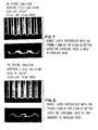
- Fig. 1 illustrates a quantitative depiction of photon density in a 1 mm photoresist layer with a via hole of optical density of 0.5, where the numbers 75, 56, 42 and 32 represent the percentage of incident dose.
- One object of the present invention is to provide a new and improved positive resist mask structure for the fabrication of semiconductor devices.
- Another object of this invention is to provide a new and improved resist structure having an enhanced R/Ro ratio where R is the dissolution rate of the exposed resist portion in solvent and Ro is the dissolution rate of .unexposed resist portions.
- Another object of this invention is to provide a new and improved positive resist structure adapted for formation of via holes having improved sidewall profiles or angles.
- Another object of this invention is to provide a new and improved positive resist structure having enhanced sensitivity to radiation.
- a further object of this invention is to provide a new and improved positive resist structure with reduced exposure time and corresponding processing throughput.
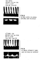
- Figs. 1 to 4 are explanatory schematic drawings for the background art.
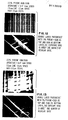
- Figs. 5 to 13 are comparative microphotographics for purposes of illustrating the invention of this application.
- a process for forming a composite resist mask on a substrate (e.g. in semiconductor device fabrication) comprising the steps of forming a first bottom layer of a blanket exposed positive resist on the substrate, and overcoating the bottom resist layer with a top layer of an unexposed positive resist containing an aromatic sensitizer such as pyrene or one of its derivatives, such as methyl pyrene.
- the top resist overcoating can be of the same composition as the bottom exposed resist layer, and optionally both being the preferred DQN resist identified above. In this manner the DQ resist can be used as the bottom exposed layer and the same DQN resist with the added sensitizer as the top layer.
- pyrene and its derivatives e.g.
- methyl pyrene have been preferred, and can be added to the DQ resist in a range of 1 to 10 wt. % and preferably from about 2 to about 4 wt. %, based on the resist solids content.
- the DQN/DQN-pyrene composite mask was found to significantly reduce the Ro of the mask.
- the composite mask After application of the composite mask, it is then image-wise exposed in a desired pattern, baked to improve adhesion and/or development, and employed for processing operations in semiconductor manufacture, after which the resist mask can be stripped from the substrate by exposure to an alkaline solvent.
- the top and bottom resist layers can be selected from commercially available diazoquinone/novolak positive resists, such as the AZ-1350 type resist of the Shipley Company.
- Examples of positive photoresists which become more soluble upon exposure to radiation are the sensitized novolak resins such as are described, for example, in US-A-3,201,239 and -3,666;473.
- the resists are applied to substrates from solvent mixtures using conventional techniques such as spraying, flowing, roller coating, spinning and dip coating, after which the solvent is removed by evaporation, which is sometimes aided by baking, to leave a layer of resist on the surface of the substrate.
- a first layer of photoresist is coated onto the substrate to be processed in a conventional manner.
- the entire resist layer is then flooded with a sufficient dose of radiation so that the photosensitive material is substantially all reacted, i.e., blanket exposed.
- the photoresist layer is then baked at a relatively high temperature to provide improved adhesion of the layer to the substrate surface.
- the baking temperatures conventionally employed to obtain improved adhesion are usually at least about 140°C. The optimum exposure times and baking times and temperatures for each photoresist can be easily determined by one skilled in the art.
- the preexposure of the bottom layer resist can be performed in two ways. First, the resist can be exposed in solution before coating on the substrate, or it can be coated first on the substrate and then exposed. The latter method was employed here, as noted above.
- a preferred diazoquinone/novolak resist comprises an o-cresol formaldehyde novolak formulated with a PAC comprised of 2,4,bis(6-diazo-5, 6-dihydro-5-oxo-l-naphthalenesulfonyloxy) benzophenone which has the structure in admixture with corresponding monoester and triester by-products.
- a second layer of a pyrene sensitized positive resist (which is preferably the same DQN resist, but which also can be different from the bottom resist layer) is then blanket coated over the bottom resist layer.
- the sensitized top resist layer can be easily formed, as for example, by adding pyrene and/or its derivatives (e.g. methyl pyrene) to the diazoquinone/novolak resists.
- the thickness of the bottom resist layer can be from about 0.5 to about 2.0 ⁇ m, and the sensitized top resist layer thickness can be in the range of about 0.4 to about 1.0 ⁇ m.
- Thermally oxidized silicon semiconductor substrates having an about 0,7 ⁇ m thick oxide layer, were coated with layers of positive resist having the thicknesses indicated in the Tables below by spin coating at a rate of 4700 rpm.
- the resists employed were.the indicated preferred DQN resists in a 30 wt. % content solution of 80 Wt. % 2-ethoxyethyl acetate, 10 wt. % n-butyl acetate and 10 wt. % xylene. A portion of these resist coated substrates were retained as controls.
- An additional number of the resist-coated substrates were blanket exposed and then overcoated with a second DQN resist containing pyrene additive sensitizer in the weight percentages indicated in the Tables below.
- the sensitized DQN resist was coated with a spin rate of about 4300 rpm as the top layer with a final thickness of about 1.0 ⁇ 0.1 ⁇ m.
- the substrates were then exposed in the Perkin-Elmer tool with UV-3 with the instrument setting: .Aperture (A) 1 or 2, slit 1 mm and scan speed (SS) as indicated in the Tables. All substrates were pre-baked for 30 minutes at 85°C on a hotplate. Additional control samples were prepared by overcoating the remaining DQN exposed substrates with the same but unexposed DQN resist.
- a pyrene sensitized DQN resist was coated directly as a single layer on the oxide surface of the semiconductor substrate, with the above- mentioned prebaking, as indicated in the Tables below.
- All substrates were then image-wise exposed in a desired pattern through a test pattern mask, and developed in a conventional alkaline developer.
- the double layer system of this invention can reduce the development time from 330s to 150s, and increase the R/Ro from 6 to 40 and the sidewall angle from 58 0 to 64 0 , respectively.
- Figures 5, 6, 7 and 8 demonstrate the significant improvement of the double layer system compared with the controls.
- R/Ro 15
- DQN- pyrene The addition of pyrene in the top DQN layer (DQN- pyrene) is a unique approach. Pyrene serves as a sensitizer to enhance the sensitivity of the diazoquinone/novolak positive resists (e.g. DQN) four times, and reduce the dissolution rate of the top resist layer which provides a good pattern mask to develop the bottom resist layer.
- DQN diazoquinone/novolak positive resists
- the double layer resist system of this invention provides an excellent resolution of 1.5 ⁇ m line-space combination, R/Ro about 15, and sidewall angle of about 70 0 , as well as the highest sensitivity ever reported for such resists at mid-UV regions (4 to about 5 times that of DQN).
- the system requires only one extra process step, with respect to the bottom resist layer.
- the blanket exposure of the bottom resist layer can be carried in solution prior to coating applications on the substrate. In fact there is indication that the blanket exposure could be omitted, since the lowest limit of blanket exposure has not been found.
- the development process is exactly the same as that for diazoquinone/novolak resists using Shipley's commercial AZ-2401 developer. Also, the system provides a convenient development time, 3 to about 4 minutes, which has a wider process window for handling, relative to development times of less than one minute for other resists.
- the sensitized top resist layer can be made thin enough to achieve the highest sensitivity, and have the total composite film thickness up to 1.0 ⁇ m (the thinner the top resist layer is, the better the pyrene is as a sensitizer, and the higher the sensitivity of the pyrene sensitized resist). Also, since the bottom layer planarizes the surface topography, images produced in the composite provide undistorted patterns over steps, Figs. 1-2 and 13.
- the exposure tool does not have to be confined to a reflective optical system such as the Perkin Elmer UV-3, but is envisioned to perform as well on refractive optical steppers, proximity printers, or contact printers.
Abstract
Description
- This invention relates to photolithography, and more particularly to the fabrication of lithographic positive resist masks for the fabrication of semiconductor integrated circuit devices.
- One positive resist system in use today for microlithography applications is comprised of an alkali soluble polymer, such as phenol or o-cresol formaldehyde novolak resin, and a diazoketone or quinone sensitizer or photoactive compound (PAC). Such sensitizers and resists are described, as for example, in US-A-3,046,118;-3,046.,121; -3,106,445; -3,201,239;-3,666,473; and -4,059,449. Exposure to radiation causes the exposed portions of the resist to become soluble in alkaline solutions in which the resist is normally developed. One method of image- wise exposing of the resist is commonly known as projection printing utilizing commercially available tools such as the Perkin-Elmer (P.E.) Projection Printer Model No. PE-300.
- In order to achieve 1:1 projection lithography, a lower exposure wavelength (e.g. 240 nm ~ 320 nm) is required, as contrasted with conventional wavelengths (e.g. 360 nm m 400 nm), as discussed by M. C. King, IEEE Tran. Elec. Devices, 26 711 (1979). A preferred resist for this application, herein referred to as "DQN", is comprised of an o-cresol formaldehyde novolak and diazoquinone PAC which is 2,4-bis(6-diazo-5,6-dihydro-5-oxo-1-naphthalenesulfonyl-oxy) benzophenone, which may be admixed with corresponding monoester and triester by-products.
- Because of the deep UV wavelengths limit of exposure sources (PE-300-UV3) and the high absorption of these resists (e.g. resin and DQN) below 300 nm, the exposure range 300-330 nm (mid-UV) is projected as being the preferred range of the coming future. The extinction coefficient, e , of PAC photoresist in the indicated DQN resist in the current exposure range (360 nm m 400 nm) is about 6x10 3 mol-1 cm-1 per diazoquinone unit. At 313 nm, which is the major output of mercury lamps in the mid-UV range, the e of the PAC is just 2.5x10³ mol-1 cm-1 per diazoquinone unit (DQ). Because of the lower of the PAC, and lower lamp intensity at 313 nm, compared with those at 360 nm, the wafer throughput (in device fabrication) exposed at 313 nm will be half or less of that of the current exposure tools.
- It has been proposed to improve the lower throughput by the addition of sensitizers, as in US-A-4,009,033 and -4,059,499, which absorb more incident dose and transfer energy to the PAC. The PAC then undergoes the direct path to the alkaline soluble product.
- Also, because of the nature of diffraction of incident radiation in the projection mode, the photons do not pass through the resist in parallel manner. This phenomenon is illustrated in Fig. 1. Because of the photon diffraction and their absorption in the photoresist, the available photon energy is not distributed homogeneously in the photoresist. Fig. 2 illustrates a quantitative depiction of photon density in a 1 mm photoresist layer with a via hole of optical density of 0.5, where the
numbers - It is known that the quantity of energy dose determines the degree of decomposition of positive resist. Consequently the decomposition of the resist determines the dissolution rate of the exposed resist. As a result, the region from the 0.75 µm depth to the 1.00 µm depth is the most difficult to be developed. This is the reason that a surface image can be easily obtained. This is illustrated in Fig. 3, where the solid and dotted lines represent the image shape if the development is stopped at the 0.75 µm depth and 1.00 µm depth, respectively. In the dissolution from the 0.75 µm to 1.0 µm depth, an isotropic loss of material occurs resulting in an undesirable image and loss (Ro) of unexposed resist.
- Instead of the shape of the dotted line in Fig. 3, it is desirable that the shape of the image would proceed anisotropically from the solid line profile to the dotted line profile of Fig. 4, as the development is continued. In this manner the value of R/Ro and sidewall angle could be increased sharply.
- In order to achieve the different dissolution ratesin vertical but not in horizontal directions, a composite combination of a pre-exposed bottom resist layer overcoated with a top layer has been proposed, for example, see US-A-3,873,313. However, several difficulties must be considered, among which is that the incorporation of an exposed bottom resist layer under the top resist layer can increase the dissolution rate of the unexposed area (Ro). Because the top resist layer of such composites, serves as a pattern layer in the development, the higher Ro will give a lower undesired R/Ro ratio.
- One object of the present invention is to provide a new and improved positive resist mask structure for the fabrication of semiconductor devices.
- Another object of this invention is to provide a new and improved resist structure having an enhanced R/Ro ratio where R is the dissolution rate of the exposed resist portion in solvent and Ro is the dissolution rate of .unexposed resist portions.
- Another object of this invention is to provide a new and improved positive resist structure adapted for formation of via holes having improved sidewall profiles or angles.
- Another object of this invention is to provide a new and improved positive resist structure having enhanced sensitivity to radiation.
- A further object of this invention is to provide a new and improved positive resist structure with reduced exposure time and corresponding processing throughput.
- For further comprehension of the-invention, and of the objects and advantages thereof, reference will be had to the following description and accompanying drawings and to the appended claims in which the novel features of the invention are more particularly set forth. In the drawings,
- Figs. 1 to 4 are explanatory schematic drawings for the background art.
- Figs. 5 to 13 are comparative microphotographics for purposes of illustrating the invention of this application.
- In accordance with this invention, a process is defined for forming a composite resist mask on a substrate (e.g. in semiconductor device fabrication) comprising the steps of forming a first bottom layer of a blanket exposed positive resist on the substrate, and overcoating the bottom resist layer with a top layer of an unexposed positive resist containing an aromatic sensitizer such as pyrene or one of its derivatives, such as methyl pyrene. Conventionally, the top resist overcoating can be of the same composition as the bottom exposed resist layer, and optionally both being the preferred DQN resist identified above. In this manner the DQ resist can be used as the bottom exposed layer and the same DQN resist with the added sensitizer as the top layer. As indicated, pyrene and its derivatives (e.g. methyl pyrene) have been preferred, and can be added to the DQ resist in a range of 1 to 10 wt. % and preferably from about 2 to about 4 wt. %, based on the resist solids content. The DQN/DQN-pyrene composite mask was found to significantly reduce the Ro of the mask.
- After application of the composite mask, it is then image-wise exposed in a desired pattern, baked to improve adhesion and/or development, and employed for processing operations in semiconductor manufacture, after which the resist mask can be stripped from the substrate by exposure to an alkaline solvent.
- The top and bottom resist layers can be selected from commercially available diazoquinone/novolak positive resists, such as the AZ-1350 type resist of the Shipley Company.
- Examples of positive photoresists which become more soluble upon exposure to radiation are the sensitized novolak resins such as are described, for example, in US-A-3,201,239 and -3,666;473. The resists are applied to substrates from solvent mixtures using conventional techniques such as spraying, flowing, roller coating, spinning and dip coating, after which the solvent is removed by evaporation, which is sometimes aided by baking, to leave a layer of resist on the surface of the substrate.
- In the process of the invention, a first layer of photoresist is coated onto the substrate to be processed in a conventional manner. The entire resist layer is then flooded with a sufficient dose of radiation so that the photosensitive material is substantially all reacted, i.e., blanket exposed. The photoresist layer is then baked at a relatively high temperature to provide improved adhesion of the layer to the substrate surface. The baking temperatures conventionally employed to obtain improved adhesion are usually at least about 140°C. The optimum exposure times and baking times and temperatures for each photoresist can be easily determined by one skilled in the art.
- The preexposure of the bottom layer resist can be performed in two ways. First, the resist can be exposed in solution before coating on the substrate, or it can be coated first on the substrate and then exposed. The latter method was employed here, as noted above.
- As indicated above, a preferred diazoquinone/novolak resist (DQN) comprises an o-cresol formaldehyde novolak formulated with a PAC comprised of 2,4,bis(6-diazo-5, 6-dihydro-5-oxo-l-naphthalenesulfonyloxy) benzophenone which has the structure

- A second layer of a pyrene sensitized positive resist (which is preferably the same DQN resist, but which also can be different from the bottom resist layer) is then blanket coated over the bottom resist layer. The sensitized top resist layer can be easily formed, as for example, by adding pyrene and/or its derivatives (e.g. methyl pyrene) to the diazoquinone/novolak resists.
- Since the photodecomposition of photoactive compounds (PAC), the electronic excited singlet state, these sensitizers meet the following effective requirements: ε > 1x10⁴ mol-1 cm -1 at 313 nm; extreme long singlet state lifetimes; high singlet state energy ( > 242 kJ/mol); and no interference with the photodecomposition of the DQ units. TheE, lifetime and energy of pyrene are 1x10⁴ mol cm , 300 ns, and 314 kJ/mol, respectively.
- The addition of these pyrene sensitizers to DQN slows the dissolution rate of R and Ro (R = exposed resist dissolution rate, Ro = unexposed resist dissolution rate). However, the lower dissolution does have advantages in terms of R/Ro. A simplified illustration is presented as follows: If R = lnm/sec and Ro = 0,2 nm/sec in the absence of the sensitizer additive, the R/Ro = 5. However, if the sensitizer additive can reduce the R and Ro by one unit, then R/Ro would be 9. Although the concept has been simplified, it should be kept in mind with respect to the additive enhancement of the diazoquinone/novolak type positive resists.
- In general, the thickness of the bottom resist layer can be from about 0.5 to about 2.0 µm, and the sensitized top resist layer thickness can be in the range of about 0.4 to about 1.0 µm.
- Thermally oxidized silicon semiconductor substrates, having an about 0,7 µm thick oxide layer, were coated with layers of positive resist having the thicknesses indicated in the Tables below by spin coating at a rate of 4700 rpm. The resists employed were.the indicated preferred DQN resists in a 30 wt. % content solution of 80 Wt. % 2-ethoxyethyl acetate, 10 wt. % n-butyl acetate and 10 wt. % xylene. A portion of these resist coated substrates were retained as controls. An additional number of the resist-coated substrates were blanket exposed and then overcoated with a second DQN resist containing pyrene additive sensitizer in the weight percentages indicated in the Tables below. The sensitized DQN resist was coated with a spin rate of about 4300 rpm as the top layer with a final thickness of about 1.0 ± 0.1 µm. The substrates were then exposed in the Perkin-Elmer tool with UV-3 with the instrument setting: .Aperture (A) 1 or 2, slit 1 mm and scan speed (SS) as indicated in the Tables. All substrates were pre-baked for 30 minutes at 85°C on a hotplate. Additional control samples were prepared by overcoating the remaining DQN exposed substrates with the same but unexposed DQN resist.
- To obtain a further control, a pyrene sensitized DQN resist was coated directly as a single layer on the oxide surface of the semiconductor substrate, with the above- mentioned prebaking, as indicated in the Tables below.
- All substrates were then image-wise exposed in a desired pattern through a test pattern mask, and developed in a conventional alkaline developer.
- The results are summarized in the following Table 'I.

- Compared with the control resist with 3 wt. %/DQN, the double layer system of this invention can reduce the development time from 330s to 150s, and increase the R/Ro from 6 to 40 and the sidewall angle from 580 to 640, respectively. Figures 5, 6, 7 and 8 demonstrate the significant improvement of the double layer system compared with the controls.
- As far as the throughput is concerned, additional samples were exposed on the P.E. unit at aperture = 1, slit 1 mm and scan speed of 720, which is four times faster than that recommended for Shipley's AZ-2400 resist. The results are summarized in the following Table II, and demonstrate that the double layer system of this invention can provide four times the throughput with R/Ro = 15, sidewall angle = 680 at a 1.5 µm line-space combination.

- As shown in Table II, the present invention provides a consistent, simple double layer mid-UV photoresist having a throughput increase of four times with better performance, R/Ro = 15, sidewall angle = 68°C at 1.5 µm line-space combination. As seen a control experiment has been carried out where the DQN resist was used as the top and bottom resist layer. However, the results show that the double DQN resist layers do not provide better performance as compared with the DQN single resist layer system. The results show that the pyrene addition in the top DQN resist layer is definitely required to make the dissolution rate change dramatically as the development reaches the bottom DQN resist layer.
- The addition of pyrene in the top DQN layer (DQN- pyrene) is a unique approach. Pyrene serves as a sensitizer to enhance the sensitivity of the diazoquinone/novolak positive resists (e.g. DQN) four times, and reduce the dissolution rate of the top resist layer which provides a good pattern mask to develop the bottom resist layer.
- Also, the double layer resist system of this invention provides an excellent resolution of 1.5 µm line-space combination, R/Ro about 15, and sidewall angle of about 700, as well as the highest sensitivity ever reported for such resists at mid-UV regions (4 to about 5 times that of DQN).
- The system requires only one extra process step, with respect to the bottom resist layer. Here, the blanket exposure of the bottom resist layer can be carried in solution prior to coating applications on the substrate. In fact there is indication that the blanket exposure could be omitted, since the lowest limit of blanket exposure has not been found.
- The development process is exactly the same as that for diazoquinone/novolak resists using Shipley's commercial AZ-2401 developer. Also, the system provides a convenient development time, 3 to about 4 minutes, which has a wider process window for handling, relative to development times of less than one minute for other resists.
- Since the bottom resist layer serves as a make-up layer, the sensitized top resist layer can be made thin enough to achieve the highest sensitivity, and have the total composite film thickness up to 1.0 ± m (the thinner the top resist layer is, the better the pyrene is as a sensitizer, and the higher the sensitivity of the pyrene sensitized resist). Also, since the bottom layer planarizes the surface topography, images produced in the composite provide undistorted patterns over steps, Figs. 1-2 and 13. The exposure tool does not have to be confined to a reflective optical system such as the Perkin Elmer UV-3, but is envisioned to perform as well on refractive optical steppers, proximity printers, or contact printers.
Claims (8)
Applications Claiming Priority (2)
| Application Number | Priority Date | Filing Date | Title |
|---|---|---|---|
| US06/454,766 US4464458A (en) | 1982-12-30 | 1982-12-30 | Process for forming resist masks utilizing O-quinone diazide and pyrene |
| US454766 | 1982-12-30 |
Publications (2)
| Publication Number | Publication Date |
|---|---|
| EP0113033A2 true EP0113033A2 (en) | 1984-07-11 |
| EP0113033A3 EP0113033A3 (en) | 1987-03-25 |
Family
ID=23805998
Family Applications (1)
| Application Number | Title | Priority Date | Filing Date |
|---|---|---|---|
| EP83111764A Withdrawn EP0113033A3 (en) | 1982-12-30 | 1983-11-24 | Process for forming resist masks |
Country Status (3)
| Country | Link |
|---|---|
| US (1) | US4464458A (en) |
| EP (1) | EP0113033A3 (en) |
| JP (1) | JPS59124134A (en) |
Families Citing this family (10)
| Publication number | Priority date | Publication date | Assignee | Title |
|---|---|---|---|---|
| US4578344A (en) * | 1984-12-20 | 1986-03-25 | General Electric Company | Photolithographic method using a two-layer photoresist and photobleachable film |
| US4571374A (en) * | 1984-12-27 | 1986-02-18 | Minnesota Mining And Manufacturing Company | Multilayer dry-film positive-acting laminable photoresist with two photoresist layers wherein one layer includes thermal adhesive |
| US4672021A (en) * | 1985-06-03 | 1987-06-09 | Fairmount Chemical Company | Contrast enhancement layer composition with naphthoquinone diazide, indicator dye and polymeric binder |
| US4863827A (en) * | 1986-10-20 | 1989-09-05 | American Hoechst Corporation | Postive working multi-level photoresist |
| US5290656A (en) * | 1988-05-07 | 1994-03-01 | Sumitomo Chemical Company, Limited | Resist composition, novel phenol compound and quinone diazide sulfonic acid ester of novel phenol compound |
| JP2661671B2 (en) * | 1989-03-20 | 1997-10-08 | 株式会社日立製作所 | Pattern forming material and pattern forming method using the same |
| JP2720224B2 (en) * | 1990-06-15 | 1998-03-04 | 富士写真フイルム株式会社 | Photosensitive lithographic printing plate |
| US6187515B1 (en) * | 1998-05-07 | 2001-02-13 | Trw Inc. | Optical integrated circuit microbench system |
| US6322953B1 (en) * | 1999-03-29 | 2001-11-27 | Winbond Electronics Corporation | Method for obtaining uniform photoresist coatings |
| GB201517273D0 (en) * | 2015-09-30 | 2015-11-11 | Univ Manchester | Resist composition |
Citations (1)
| Publication number | Priority date | Publication date | Assignee | Title |
|---|---|---|---|---|
| US3873313A (en) * | 1973-05-21 | 1975-03-25 | Ibm | Process for forming a resist mask |
Family Cites Families (23)
| Publication number | Priority date | Publication date | Assignee | Title |
|---|---|---|---|---|
| US2937085A (en) * | 1954-01-11 | 1960-05-17 | Ditto Inc | Composite photosensitive plate, and method of making printing plate therefrom |
| BE563723A (en) * | 1957-01-04 | |||
| US3317320A (en) * | 1964-01-02 | 1967-05-02 | Bendix Corp | Duo resist process |
| US3380825A (en) * | 1964-11-27 | 1968-04-30 | Du Pont | Process for producing images |
| US3486900A (en) * | 1965-06-02 | 1969-12-30 | Keuffel & Esser Co | Diazotype material |
| US3482977A (en) * | 1966-02-11 | 1969-12-09 | Sylvania Electric Prod | Method of forming adherent masks on oxide coated semiconductor bodies |
| US3518084A (en) * | 1967-01-09 | 1970-06-30 | Ibm | Method for etching an opening in an insulating layer without forming pinholes therein |
| US3634082A (en) * | 1967-07-07 | 1972-01-11 | Shipley Co | Light-sensitive naphthoquinone diazide composition containing a polyvinyl ether |
| US3567453A (en) * | 1967-12-26 | 1971-03-02 | Eastman Kodak Co | Light sensitive compositions for photoresists and lithography |
| US3549368A (en) * | 1968-07-02 | 1970-12-22 | Ibm | Process for improving photoresist adhesion |
| US3591378A (en) * | 1968-07-31 | 1971-07-06 | Eastman Kodak Co | Process for making positive-working relief plate |
| US3716390A (en) * | 1970-05-27 | 1973-02-13 | Bell Telephone Labor Inc | Photoresist method and products produced thereby |
| US3827908A (en) * | 1972-12-11 | 1974-08-06 | Ibm | Method for improving photoresist adherence |
| US4036644A (en) * | 1973-03-16 | 1977-07-19 | International Business Machines Corporation | Photoresist process and photosensitive O-quinone diazide article with aliphatic carboxylic acid as adhesion promotor |
| US3982943A (en) * | 1974-03-05 | 1976-09-28 | Ibm Corporation | Lift-off method of fabricating thin films and a structure utilizable as a lift-off mask |
| US3955981A (en) * | 1975-01-06 | 1976-05-11 | Zenith Radio Corporation | Method of forming electron-transmissive apertures in a color selection mask by photoetching with two resist layers |
| US4009033A (en) * | 1975-09-22 | 1977-02-22 | International Business Machines Corporation | High speed positive photoresist composition |
| US4088490A (en) * | 1976-06-14 | 1978-05-09 | International Business Machines Corporation | Single level masking process with two positive photoresist layers |
| GB1604652A (en) * | 1977-04-12 | 1981-12-16 | Vickers Ltd | Radiation sensitive materials |
| GB1578259A (en) * | 1977-05-11 | 1980-11-05 | Philips Electronic Associated | Methods of manufacturing solid-state devices apparatus for use therein and devices manufactured thereby |
| US4212935A (en) * | 1978-02-24 | 1980-07-15 | International Business Machines Corporation | Method of modifying the development profile of photoresists |
| US4237216A (en) * | 1978-12-08 | 1980-12-02 | International Business Machines Corporation | Photosensitive patternable coating composition containing novolak type materials |
| US4352870A (en) * | 1979-11-27 | 1982-10-05 | Bell Telephone Laboratories, Incorporated | High resolution two-layer resists |
-
1982
- 1982-12-30 US US06/454,766 patent/US4464458A/en not_active Expired - Lifetime
-
1983
- 1983-08-18 JP JP58149745A patent/JPS59124134A/en active Granted
- 1983-11-24 EP EP83111764A patent/EP0113033A3/en not_active Withdrawn
Patent Citations (1)
| Publication number | Priority date | Publication date | Assignee | Title |
|---|---|---|---|---|
| US3873313A (en) * | 1973-05-21 | 1975-03-25 | Ibm | Process for forming a resist mask |
Non-Patent Citations (5)
| Title |
|---|
| CHEMICAL ABSTRACTS, vol. 62, no. 7, 29th March 1965, column no. 7938e, Columbus, Ohio, US; H. HEUSINGER: "Sensitization by aromatic additives of the chain cross-linking in polystyrene under the action of ionizing radiation", & RADIOCHIM. ACTA 3(1/2), 7-13(1964) * |
| IBM TECHNICAL DISCLOSURE BULLETIN, vol. 21, no. 7, December 1978, pages 2969,2970, New York, US; A.R. GUTIERREZ et al.: "Lithographic applications of pyrene and anthracene derivatives of naphthoquinone-1,2-diazide as radiation-sensitive compounds" * |
| IBM TECHNICAL DISCLOSURE BULLETIN, vol. 26, no. 4, September 1983, pages 1955-1959, New York, US; M. CHOW et al.: "Photosensitization of diazonaphthoquinone/novolak resists" * |
| JOURNAL OF THE AMERICAN CHEMICAL SOCIETY, vol. 86, no. 21, November 1964, pages 4537-4540, Gaston, PA, US; W.G. HERKSTROETER et al.: "Mechanisms of photochemical reactions in solution. XXVIII. Values of triplet excitation energies of selected sensitizers" * |
| PHOTOGRAPHIC SCIENCE AND ENGINEERING, vol. 19, no. 3, May/June 1975, pages 173-175, Society of Photographic Scientists and Engineers, Springfield, VA, US; T.A. SHANKOFF et al.: "On the spectral sensitization of negative and positive photoresists" * |
Also Published As
| Publication number | Publication date |
|---|---|
| EP0113033A3 (en) | 1987-03-25 |
| JPH0143298B2 (en) | 1989-09-20 |
| US4464458A (en) | 1984-08-07 |
| JPS59124134A (en) | 1984-07-18 |
Similar Documents
| Publication | Publication Date | Title |
|---|---|---|
| US8846296B2 (en) | Photoresist compositions | |
| EP1240553A2 (en) | Photoresist composition for deep uv radiation | |
| US5215856A (en) | Tris-(hydroxyphenyl) lower alkane compounds as sensitivity enhancers for o-quinonediazide containing radiation-sensitive compositions and elements | |
| EP1478978B1 (en) | Self-aligned pattern formation using dual wavelengths | |
| US4985344A (en) | Radiation imaging process for forming pattern without alkali-soluble polymer underlayer and water soluble radiation-sensitive diazonium salt overlayer | |
| US4464458A (en) | Process for forming resist masks utilizing O-quinone diazide and pyrene | |
| US4797348A (en) | Method of forming a positive resist pattern in photoresist of o-naphthoquinone diazide and bisazide with UV imaging exposure and far UV overall exposure | |
| JPH0650396B2 (en) | Positive photoresist composition | |
| JP3078153B2 (en) | Photosensitive composition | |
| US6106995A (en) | Antireflective coating material for photoresists | |
| US5108870A (en) | Positive-working photoresist composition containing purified broadband dye and process of using | |
| EP0573220B1 (en) | Dyed i-line positive-working radiation sensitive mixtures | |
| US5719004A (en) | Positive photoresist composition containing a 2,4-dinitro-1-naphthol | |
| KR910005031B1 (en) | Photo sensitive composition | |
| JPH0210348A (en) | Formation of positive type photosensitive composition and resist pattern | |
| JPH07271037A (en) | Positive ionization-sensitive radioactive resin composition | |
| JPH0786127A (en) | Formation of resist pattern | |
| JPH0527441A (en) | Photo-or radiation-sensitive composition, pattern forming method, production of photomask, and production of semiconductor device | |
| JPH0343614B2 (en) | ||
| JPH07134416A (en) | Radiation sensitive resin composition | |
| US5281508A (en) | Positive-working photoresist containing o-naphthoquinone diazide sulfonic acid ester and novolak resin consisting of 35 to 43% m-cresol and 65 to 57% p-cresol with substantial absence of o-cresol | |
| JPS63282734A (en) | Positive type photoresist composition | |
| EP0788620B1 (en) | Positive photosensitive composition | |
| JP3079195B2 (en) | Developer for positive-type radiation-sensitive resist | |
| US5306595A (en) | Composition containing naphthoquinone diazide sulfonic acid mixed esters and radiation-sensitive recording material prepared therewith |
Legal Events
| Date | Code | Title | Description |
|---|---|---|---|
| PUAI | Public reference made under article 153(3) epc to a published international application that has entered the european phase |
Free format text: ORIGINAL CODE: 0009012 |
|
| AK | Designated contracting states |
Designated state(s): DE FR GB |
|
| 17P | Request for examination filed |
Effective date: 19841029 |
|
| PUAL | Search report despatched |
Free format text: ORIGINAL CODE: 0009013 |
|
| AK | Designated contracting states |
Kind code of ref document: A3 Designated state(s): DE FR GB |
|
| 17Q | First examination report despatched |
Effective date: 19881017 |
|
| STAA | Information on the status of an ep patent application or granted ep patent |
Free format text: STATUS: THE APPLICATION HAS BEEN WITHDRAWN |
|
| 18W | Application withdrawn |
Withdrawal date: 19890223 |
|
| RIN1 | Information on inventor provided before grant (corrected) |
Inventor name: MOREAU, WAYNE MARTIN Inventor name: CHOW, MING-FEA Inventor name: FREDERICKS, EDWARD CARMINE |