EP0112028B1 - Electrically connected and electrically interconnected large area photovoltaic cells and method of producing said cells - Google Patents
Electrically connected and electrically interconnected large area photovoltaic cells and method of producing said cells Download PDFInfo
- Publication number
- EP0112028B1 EP0112028B1 EP83306832A EP83306832A EP0112028B1 EP 0112028 B1 EP0112028 B1 EP 0112028B1 EP 83306832 A EP83306832 A EP 83306832A EP 83306832 A EP83306832 A EP 83306832A EP 0112028 B1 EP0112028 B1 EP 0112028B1
- Authority
- EP
- European Patent Office
- Prior art keywords
- large area
- electrically
- cell
- cells
- busbars
- Prior art date
- Legal status (The legal status is an assumption and is not a legal conclusion. Google has not performed a legal analysis and makes no representation as to the accuracy of the status listed.)
- Expired
Links
Images


Classifications
-
- H—ELECTRICITY
- H10—SEMICONDUCTOR DEVICES; ELECTRIC SOLID-STATE DEVICES NOT OTHERWISE PROVIDED FOR
- H10F—INORGANIC SEMICONDUCTOR DEVICES SENSITIVE TO INFRARED RADIATION, LIGHT, ELECTROMAGNETIC RADIATION OF SHORTER WAVELENGTH OR CORPUSCULAR RADIATION
- H10F19/00—Integrated devices, or assemblies of multiple devices, comprising at least one photovoltaic cell covered by group H10F10/00, e.g. photovoltaic modules
- H10F19/90—Structures for connecting between photovoltaic cells, e.g. interconnections or insulating spacers
-
- H—ELECTRICITY
- H10—SEMICONDUCTOR DEVICES; ELECTRIC SOLID-STATE DEVICES NOT OTHERWISE PROVIDED FOR
- H10F—INORGANIC SEMICONDUCTOR DEVICES SENSITIVE TO INFRARED RADIATION, LIGHT, ELECTROMAGNETIC RADIATION OF SHORTER WAVELENGTH OR CORPUSCULAR RADIATION
- H10F10/00—Individual photovoltaic cells, e.g. solar cells
- H10F10/10—Individual photovoltaic cells, e.g. solar cells having potential barriers
- H10F10/17—Photovoltaic cells having only PIN junction potential barriers
- H10F10/172—Photovoltaic cells having only PIN junction potential barriers comprising multiple PIN junctions, e.g. tandem cells
-
- H—ELECTRICITY
- H10—SEMICONDUCTOR DEVICES; ELECTRIC SOLID-STATE DEVICES NOT OTHERWISE PROVIDED FOR
- H10F—INORGANIC SEMICONDUCTOR DEVICES SENSITIVE TO INFRARED RADIATION, LIGHT, ELECTROMAGNETIC RADIATION OF SHORTER WAVELENGTH OR CORPUSCULAR RADIATION
- H10F19/00—Integrated devices, or assemblies of multiple devices, comprising at least one photovoltaic cell covered by group H10F10/00, e.g. photovoltaic modules
- H10F19/30—Integrated devices, or assemblies of multiple devices, comprising at least one photovoltaic cell covered by group H10F10/00, e.g. photovoltaic modules comprising thin-film photovoltaic cells
- H10F19/31—Integrated devices, or assemblies of multiple devices, comprising at least one photovoltaic cell covered by group H10F10/00, e.g. photovoltaic modules comprising thin-film photovoltaic cells having multiple laterally adjacent thin-film photovoltaic cells deposited on the same substrate
- H10F19/35—Structures for the connecting of adjacent photovoltaic cells, e.g. interconnections or insulating spacers
-
- H—ELECTRICITY
- H10—SEMICONDUCTOR DEVICES; ELECTRIC SOLID-STATE DEVICES NOT OTHERWISE PROVIDED FOR
- H10F—INORGANIC SEMICONDUCTOR DEVICES SENSITIVE TO INFRARED RADIATION, LIGHT, ELECTROMAGNETIC RADIATION OF SHORTER WAVELENGTH OR CORPUSCULAR RADIATION
- H10F71/00—Manufacture or treatment of devices covered by this subclass
- H10F71/10—Manufacture or treatment of devices covered by this subclass the devices comprising amorphous semiconductor material
- H10F71/103—Manufacture or treatment of devices covered by this subclass the devices comprising amorphous semiconductor material including only Group IV materials
-
- H—ELECTRICITY
- H10—SEMICONDUCTOR DEVICES; ELECTRIC SOLID-STATE DEVICES NOT OTHERWISE PROVIDED FOR
- H10F—INORGANIC SEMICONDUCTOR DEVICES SENSITIVE TO INFRARED RADIATION, LIGHT, ELECTROMAGNETIC RADIATION OF SHORTER WAVELENGTH OR CORPUSCULAR RADIATION
- H10F77/00—Constructional details of devices covered by this subclass
- H10F77/93—Interconnections
- H10F77/933—Interconnections for devices having potential barriers
- H10F77/935—Interconnections for devices having potential barriers for photovoltaic devices or modules
- H10F77/937—Busbar structures for modules
-
- Y—GENERAL TAGGING OF NEW TECHNOLOGICAL DEVELOPMENTS; GENERAL TAGGING OF CROSS-SECTIONAL TECHNOLOGIES SPANNING OVER SEVERAL SECTIONS OF THE IPC; TECHNICAL SUBJECTS COVERED BY FORMER USPC CROSS-REFERENCE ART COLLECTIONS [XRACs] AND DIGESTS
- Y02—TECHNOLOGIES OR APPLICATIONS FOR MITIGATION OR ADAPTATION AGAINST CLIMATE CHANGE
- Y02E—REDUCTION OF GREENHOUSE GAS [GHG] EMISSIONS, RELATED TO ENERGY GENERATION, TRANSMISSION OR DISTRIBUTION
- Y02E10/00—Energy generation through renewable energy sources
- Y02E10/50—Photovoltaic [PV] energy
- Y02E10/548—Amorphous silicon PV cells
-
- Y—GENERAL TAGGING OF NEW TECHNOLOGICAL DEVELOPMENTS; GENERAL TAGGING OF CROSS-SECTIONAL TECHNOLOGIES SPANNING OVER SEVERAL SECTIONS OF THE IPC; TECHNICAL SUBJECTS COVERED BY FORMER USPC CROSS-REFERENCE ART COLLECTIONS [XRACs] AND DIGESTS
- Y02—TECHNOLOGIES OR APPLICATIONS FOR MITIGATION OR ADAPTATION AGAINST CLIMATE CHANGE
- Y02P—CLIMATE CHANGE MITIGATION TECHNOLOGIES IN THE PRODUCTION OR PROCESSING OF GOODS
- Y02P70/00—Climate change mitigation technologies in the production process for final industrial or consumer products
- Y02P70/50—Manufacturing or production processes characterised by the final manufactured product
Definitions
- This invention relates generally to large area photovoltaic cells and more particularly to electrically interconnected large area photovoltaic cells. Also disclosed are the methods of producing said electrically-interconnected, large area photovoltaic cells.
- Described herein are adjacent, electrically interconnected, large area photovoltaic cells. Also discussed is the fabrication of a large area photovoltaic cell from the plurality of electrically isolated, small area segments which must be electrically-interconnected to provide an electrically operable large area solar cell and the fabrication of a plurality of adjacent, electrically-interconnected, large area solar cells from a plurality of discrete large area photovoltaic cells.
- Patents Abstracts of Japan volume 5, No. 153 (E-76), 26th September 1981 and Patents Abstracts of Japan Volume 5, No. 133 (E-71), 25th August 1981 disclose a large area photovoltaic cell comprising a plurality of small area segments sharing a common substrate and further including a plurality of semiconductor layers atop one surface of the substrate, with a transparent conductive coating atop the semiconductor layers.
- a plurality of busbars are connected to the small area segments and each of the busbars terminates on the same portion of the large area cell.
- Means are provided for electrically connecting the busbars and these means, together with the substrate, provide the output electrodes of the cell.
- crystal silicon devices are the basis of a huge semiconductor industry, devices made from crystal silicon have fixed parameters which are not variable as desired, require large amounts of materials, are only producible in relatively small areas and are expensive and time consuming to produce.
- Devices based upon amorphous silicon can eliminate these crystal silicon disadvantages.
- Amorphous silicon has an optical absorption edge having properties similar to a direct gap semiconductor and only a material thickness of one micrometer or less is necessary to absorb the same amount of sunlight as the 50pm thick cyrstalline silicon. Further, amorphous silicon can be made faster and more easily in larger areas than can cyrstalline silicon.
- the activated fluorine readily diffuses into and bonds to the amorphous silicon in the amorphous body to substantially decrease the density of localized defect states therein, because the small size of the fluorine atoms enables them to be readily introduced into the amorphous body.
- Fluorine is considered to be a more efficient compensating or altering element than hydrogen when employed alone or with hydrogen because of its exceedingly small size, high reactivity, specificity in chemical bonding, and highest electronegativity.
- the tandem cell device has two or more cells with the light directed serially through each cell, with a large band gap material followed by a smaller band gap material to absorb the light passed through the first cell or layer. By substantially matching the generated currents from each cell, the overall open circuit voltage of each cell may be added, thereby producing a device which makes full use of the energy produced by incoming light.
- amorphous silicon alloys can be deposited in multiple layers over relatively large area substrates to form solar cells in a high volume, continuous processing system.
- Continuous processing systems of this kind are disclosed, for example, in pending patent applications: Serial No. 151,301, (Pat. No. 4400409), for A Method of Making P-Doped Silicon Films and Devices Made Therefrom; Serial No. 244 386, filed March. 16, 1981 for Continuous Systems For Depositing Amorphous Semiconductor Material; Serial No. 240,493, filed March 16, 1981 for Continuous Amorphous Solar Cell Production System; EPA No.
- a substrate may be continuously advanced through successive triads of deposition chambers, wherein each chamber is dedicated to the deposition of a specific material.
- each chamber is dedicated to the deposition of a specific material.
- the first chamber of each triad is dedicated for depositing a p-type amorphous semiconductor material
- the second chamber of each triad is dedicated for depositing an intrinsic semiconductor material
- the third chamber of each triad is dedicated for depositing an n-type amorphous semiconductor material.
- the resultant roll of large area photovoltaic cells manufactured by the mass production glow discharge deposition technique described hereinabove comprises an elongated strip of substrate upon which successive semiconductor layers are deposited. It is well known that following the deposition of the semiconductor layers, a further step must be performed in order to complete fabrication of an operable, semiconductor device. In this step, a transparent, electrically conductive coating, which is characterised by high light- transmissivity and high electrical-conductivity, is deposited atop the semiconductor body.
- This elongated roll of photovoltaic material must now be processed to form therefrom a plurality of large area photovoltaic cells adapted for either series or parallel electrical interconnections.
- a plurality of electrically interconnected large area photovoltaic cells each cell comprising a plurality of electrically-isolated, small area segments which share a common electrically conductive substrate upon which a plurality of continuous semiconductor layers are deposited; a plurality of spaced, electrically-conductive busbars disposed atop and electrically insulated from the surface therebeneath, said busbars electrically interconnected to the small area segments of said discrete large area cells; each small area segment being defined by a discrete portion of a transparent conductive coating atop the semiconductor layers, whereby each small area segment is electrically isolated from other small area segments; and wherein each of the busbars of each large area cell terminates on the same portion of the surface of the associated large area cell; said electrically interconnected cells comprising, in combination: an electrically insulating layer applied to the busbar terminating portion of each large area cell to prevent short circuiting; first connecting means (38) for electrically connecting the busbars of each discrete large area cell; at
- the busbars of each discrete large area cells may terminate within a peripheral border portion of that cell. Electrical access to the substrate may be provided either by electrically-conductive rivets secured within the peripheral border portion of that cell or by an exposed section of the peripheral border portion. In either event, the substrate is sufficiently accessible to provide for series or parallel electrical connection of adjacent large area cells.
- a stacked, tandem or cascade-type, photovoltaic cell formed of successive p-i-n layers, each layer formed from an amorphous semiconductor alloy and including an transparent, conductive coating, is shown generally by the reference numeral 10.
- the methods described herein are not limited solely to the production of stacked p-i-n photovoltaic cells, but are of equal value in the production of improved Schottky or improved MIS (metal-insulator-semiconductor) type cells or simply the production of improved semiconductor devices. Regardless of cell type, the large area cells and the production techniques which are detailed in this specification find utility with photovoltaic cells formed with layers of semiconductor materials and with a transparent transparent, conductive layer deposited atop the semiconductor layers.
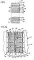
- Figure 1 shows a plurality of p-i-n solar cells 12a, 12b, and 12c.
- a substrate 11 which may be a transparent conductive layer or formed from a metallic surface foil. Since certain applications may require a thin oxide layer and/or a series of base contacts prior to the application of the semiconductor material, for the purpose of this application the term substrate shall include not only a flexible film but also any elements added thereto by preliminary processing.
- the substrate 11 may be formed of stainless steel, aluminum, tantalum, molybdenum, or chrome. However, other materials may be used, including, specifically, a glass insulating base having an electrically conductive layer applied thereon.
- Each of the cells 12a, 12b and 12c include a semiconductor body containing in one embodiment, at least a silicon alloy.
- Each of the alloy bodies includes an n-type conductivity semiconductor or layer 20a, 20b and 20c; an intrisic semiconductor layer 18a, 18b, and 18c; and a p-type conductivity semiconductor or layer 16a, 16b and 16c.
- cell 12b is an intermediate cell and, as indicated in Figure 1, additional intermediate cells may be stacked upon the illustrated cells.
- an amorphous semiconductor alloy which includes fluorine is used to form each of the layers of the cells 12, the layers could also be formed of crystalline or polycrystalline materials, with orwithoutthe addition of fluorine.
- inventive concepts disclosed herein are applicable to photovoltaic cells, regardless of materials or crystallinity.
- the p-type semiconductor layers 16a, 16b, 16c are ideally low light absorption, high conductivity layers.
- the intrisic semiconductor layers 18a, 18b, 18c are characterized by an adjusted wavelength threshold for a solar photoresponse, high light absorption, low dark conductivity, and high photoconductivity, and include sufficient amounts of a band gap adjusting element or elements to optimize the band gap for the particular cell application.
- the intrisic layers are band gap adjusted to provide cell 12a with'a lowest band gap, cell 12c with the highest band gap, and cell 12bwith a band gap between the other two.
- the n-type layers 20a, 20b, and 20c are,,gharacterized by low light absorption, high conductivity alloy materials.
- Thethickness of the band gap adjusted amorphous intrinsic alloy layer is preferably between about 2000 angstroms to 3,000 angstroms.
- the thickness of the p-type layers is preferably between 50 to 500 angstroms. Due to the shorter diffusion length of the holes, the p-type layers generally will be as thin as possible. Further, the outermost layer, here the p-type layer 20c, will be as thin as possible to avoid absorption of light and need not include the band gap adjusting element or elements.
- a further deposition step is performed.
- a continuous or discontinous, transparent, conductive layer 22 of high electrical conduction and high light transmissivity is added atop the n-type layer 20c.
- This transparent, conductive layer 22 may, for example, be a thin 500 angstrom thick film of indium tin oxide, (ITO), cadmium stannate (Cd 2pSn0 4 ⁇ ), or doped tin oxide (Sn0 2p).
- grid patterns 24 are routinely added to the transparent, conductive material, for applications involving a sufficiently small area solar cell, the transparent, conductive coating 22 is generally sufficiently conductive so a grid pattern 24 is not necessary.
- a grid pattern 24 is applied atop the transparent, conductive layer 22 to shorten the carrier path and increase the conduction efficiency thereof.
- This transparent, conductive layer 22 being applied directly atop the semiconductor layers, serves as a top electrode for the photovoltaic device 10, with the conductive substrate 11 serving as a bottom electrode. Since the transparent, conductive layer 22 electrically communicates with the semiconductor layers therebelow, in the preferred embodiment, the application of a relatively thick insulating layer between the semiconductor layers and the transparent, conductive layer 22 can be used to divide the large area (one square foot) solar cell into a plurality (180) small area segments thereof for reasons which will become clear hereinafter.
- the insulating material is applied over the surface area of the semiconductor layers so as to divide the surface thereof into a plurality of rows and columns of insulating material.
- the transparent, conductive layer 22 is subsequently deposited onto the surface of the semiconductor layers, it can only electrically communicate with those segments not covered by insulating material. Electrically-isolated, electrically-insulated, portions of semiconductor material may be thereby fabricated.
- Figure 2a is a fragmentary view of the upper surface of the transparent, conductive coating 22 applied atop the semiconductor layers of the solar cell 10.
- the surface area of the semiconductor layers of the solar cell material 10 may be divided into a plurality of electrically-isolated segments 26 in any one of a plurality of methods which will be described hereinafter.
- the exact number and arrangement of the isolated segments 26 of the solar cell 10 may vary, in the preferred embodiment, twelve (12) parallel rows of fifteen (15) isolated segments 26 (a total of one hundred-eighty subcells) define the surface area of each large area (one square foot) solar cell.
- isolated segment is defined herein as a small surface area segment of a large area solar cell which is electrically-isolated from other segments of the surface area of the large area solar cell, but which shares a common substrate or electrode with those other segments.
- the isolated segments 26 are formed, in the preferred embodiment, by discrete portions of the , transparent, conductive coating 22 deposited atop the semiconductor layers of the solar cell material 10. Each isolated segment 26 may also be formed from the transparent, conductive coating 22 by other known methods such as photo- lithographing and chemical etching. For instance, a photoresist solution may be applied to the surface of the transparent, conductive coating 22 and pre-heated to dry off solvents, thus leaving a thin film as a residue.
- the grid pattern 24 is then laid over the residual film, and those portions of the film not covered by the pattern are exposed to electro-magnetic radiation, typically in the ultra-violet region of the spectrum, or to a beam of electrons of appropriate energy to develop the film.
- electro-magnetic radiation typically in the ultra-violet region of the spectrum
- a beam of electrons of appropriate energy to develop the film.
- the exposed portions (positive resist) or the unexposed portions (negative resist) of the film and the underlying transparent, conductive coating 22 are removed.
- the residual photoresist film is washed with a solvent to remove same from the surface of the transparent, conductive coating 22.
- a grid pattern 24 may now be applied onto the surface of the now isolated segments 26 of the transparent, conductive coating 22.
- the isolated segments 26 of the solar cell material 10 can be formed by dividing the transparent, conductive coating 22 into a plurality of discrete segments 22a-22u without applying a grid pattern thereonto. It is to be understood that for purposes of this description, the numeral 26 will refer to isolated segments of the transparent, conductive coating with a grid pattern applied thereonto, while the numerals 22a-22u refer to isolated segments of the transparent, conductive coating 22 not having the grid pattern applied thereonto.
- the discrete segments 22a-22u may be formed either by originally depositing the transparent, conductive coating 22 in a discontinuous fashion, as by the application of the insulating material as previously described, or by depositing a continuous transparent, conductive coating 22 and then removing intermediate parts by the photolithography and etching techniques previously described. Note that the electrically-insulating material may be applied atop the semiconductor layers by means of screen printing or other known techniques.
- Each isolated segment, whether formed by a continuous or discontinuous transparent, conductive coating may have a grid pattern 24 applied thereonto.
- the width dimension of each grid pattern 24 is defined by a plurality of substantially equally spaced, relatively thin, parallel, electrically-conductive lines 30 radiating perpendicularly from both sides of a tapered, relatively thick, electrically-conductive, busbar-connecting line 32 which defines the length dimension of the grid pattern 24.
- the grid patterns 24 are formed are formed so as to maximize the current collected from the solar cell material while minimizing the amount of light prevented from entering the solar cell material.
- the arrangement of isolated segments 26, the length and width dimensions of the grid patterns 24 and the isolated segments 26, the number of parallel lines 30, the number of parallel rows of the isolated segments 26, the total number of isolated segments 26 formed on a large area solar cell and hence, the size and configuration of that solar cell may vary without departing from the scope of the present invention.
- the grid patterns 24 may be printed, by any well known technique, such as screen printing, onto the transparent, conductive segments 26 with an electrically conductive material such as silver paste.
- the term “scribing” is intended to encompass all such methods of removing the transparent, conductive coating 22, which include, but are not limited to: (a) chemical etching; (b) plasma etching; (c) various laser techniques; (d) a waterjet technique; or (e) applying the transparent, conductive coating with a mask to form said distinct, discontinuous segments.
- each isolated segment of the solar cell material 10 may be individually tested to determine whether the electrical output therefrom is sufficient to render it "electrically operative” or " electrically operable".
- the terms “electrically operative isolated segment” or “electrically operable isolated segment” refer to those isolated segments 26 of the solar cell material which 10 provide satisfactory electrical output.
- the electrical connection of isolated segments 26 of the solar cell material 10 providing unsatisfactory electrical output reduces the overall efficiency of the solar cell material. Further, since the isolated segments 26 of large area solar cells are connected in parallel, the electrical connection of any isolated segment 26 on a large area solar cell providing a very low voltage output could significantly decrease the electrical output of the entire large area solar cell 10.
- the electrical connections disclosed herein are not limited to large area solar cells, which include small area segments, but may also be used with undivided large area cells.
- a plurality of elongated, copper, electrically conductive busbars 34 are affixed to the surface of the semiconductor layers with an electrically-insulating silicon adhesive.
- the silicon adhesive is applied as a very thin layer because the busbars 34 are to be positioned between alternate rows of isolated segments 26 of the solar cell material. In other words, even after the busbars 34 are affixed to the solar cell material 10, a lateral gap must remain between the adjacent discrete segments 26 of the transparent, conductive coating 26 and the associated busbar 34.
- six conductive busbars 34 about 1/10 of an inch wide and .03 of an inch thick, are employed.
- the busbar-connecting line 32 from each electrically-operative isolated segment 26 of the solar cell material is electrically-connected to an adjacent busbar 34 using a dot of electrically-conductive material such as silver paste 35. Those isolated segments 26 whose electrical output falls below the selected minimum satisfactory level remain electrically-isolated, by the insulating silicon adhesive, from the electrically-conductive copper busbar 34.
- the foregoing sequence may be reversed and, in fact, once the incidence of electrically-operative, isolated segments 26 routinely exceeds a predetermined level, the testing step may be omitted. In such cases, it is actually desirable to reverse the sequence and adhesively secure the copper busbars 34 to the surface of transparent, conductive coating 22 prior to printing the grid patterns 24 onto the isolated segments 26. This reversed sequence is preferable because the grid patterns 24 and the electrical connections thereof to the copper busbars 34 may be simultaneously accomplished. Although the sequence is not important from an operational standpoint, it is significant from an assembly line standpoint where the elimination of a step can represent important economic gains.
- FIGs 3a, 3b, 4a, 4b, 5a and 5b are fragmentary views illustrating the top surface of adjacent large area photovoltaic cells 10 and specifically showing the manner in which said large area cells are electrically interconnected pursuant to the teachings of this invention. More particularly, depicted therein are portions of electrically interconnected large area photovoltaic cells such as 10a and 10b, and in the case of Figures 5a and 5b, cell 10c. Although different methods of connecting these large area cells are shown in the Figures, the same reference numeral:will depict common elements in each of the embodiments. It is to be understood that each of the photovoltaic cells 10 are preferably formed of a plurality of electrically isolated, small area segments which will be generally referred to by the reference numeral 26.
- each electrically-isolated segment 26 is capable of functioning as a photovoltaic device independent of every other segment 26, the present invention deals with the electrical interconnection of (1) these electrically-isolated segments 26 to obtain an overall electrical output from the large area solar cell 10 which is the sum of the output of each isolated segment 26, and (2) adjacent large area solar cells, such as 10a and 10b, to obtain an electrical output which is the sum of the output of each electrically-interconnected large area cell, such as 10a and 10b.
- each of the copper busbars 34 extends beyond the periphery of the active area of each large area photovoltaic cell and terminates on an upper peripheral border portion 36.
- active area is defined as that portion of the large area photovoltaic cell 10 which includes electrically communicating substrate, semiconductor and transparent, conductive coating layers
- the "same portion" of the large area cell 10 is defined as any continuous segment of the surface of the cell without regard to shape or size.
- An electrically-insulating layer of any well known type must be applied below the busbars 34 on the border portion 36 to be sure that (1) said portion (36) is electrically "inactive", and (2) the busbars 34 do not electrically contact and consequently short circuit current to the substrate 11.
- the electrically-insulating layer may be applied in any well known manner, such as by depositing an insulating coating simultaneously with the application of the electrically-insulating material which forms the electrically-isolated small area segments of each of the large area cells 10.
- each large area photovoltaic cell Having electrically interconnected the electrically-operable, electrically-isolated segments 26 of the large area photovoltaic cells 10a and 10b, to the busbars 34a, 34b and 34c, respectively, and having electrically insulated those busbars from the substrate 11 on the electrically insulated peripheral border portion 36 of the cells 10a and 10b, it is necessary to electrically interconnect the busbars of each large area cell in order to provide a single electrode therefrom.
- the lower or base electrode of each large area photovoltaic cell such as, 10a and 10b, is provided by the common substrate 11.
- the electrically-isolated segments 26 of the large area cell 10a share a common base electrode or substrate 11.
- a section 11 a of the upper left hand corner of the upper peripheral border portion 36 of the large area photovoltaic cell 10a is exposed and is therefor adapted to provide electrical access to the common substrate 11.
- two distal sections 11a of the peripheral border portion 36 are exposed to provide electrical access to the common substrate 11.
- the exposed substrate sections 11 a may be formed by burnishing the previously deposited semiconductor layers, or they may be formed by masking a portion of the peripheral border during the deposition of semiconductor layers, or by etching those semiconductor layers from the substrate, or by any other commonly employed technique.
- electrical access to the substrate is provided in Figures 5a and 5b by plated copper rivets 48.
- the copper rivets preferably include surrated washers for establishing good electrical contact with the substrate 11.
- One such rivet 48 is secured to each large area cell 10a, 10b and 10c for the series connection shown in Figure 5a, while two rivets 48 are secured to the large area cells 10a, 10b and 10c for the parallel connection shown in Figure 5b.
- this strip comprises an inner metallic core made of an electrically-conductive material such as nickel- plated copper, protected by a surrounding, electrically-insulating jacket such as glass-filled teflon, polyvinylcholoride, vinylacetate, or other like flexible, dielectric material.
- a surrounding, electrically-insulating jacket such as glass-filled teflon, polyvinylcholoride, vinylacetate, or other like flexible, dielectric material.
- a length of the conductive strip 38 is electrically connected to the busbars 34 by punching holes through the strip 38 at positions, which, when the strip is applied atop the peripheral border portion 36 of the large area cell 10a, will present the metallic core thereof to each busbar 34a and 34b.
- the holes in the conductive strip 38 are formed to directly overlie each busbar 34 of each large area cell 10.
- the strip 38 is then securely electrically connected to each of the busbars, 34a and 34b, on that large area cell, such as 10a, by means of a solder joint 40.
- the busbars, such as 34c of large area cell 10b are electrically interconnected by a length of conductive strip 38.
- the portion of the insulating jacket of the strip 38 immediately overlying each of the busbars may be stripped away and the exposed, conductive core thereof directly fastened, as by soldering, to the busbars.
- electrically-conductive metallic wires 42 may be soldered, as at 44, to each of the ends of those strips 38, the conductive core having first been exposed at said ends.
- the metallic wires 42 may be electrically connected, as by weld joints 45, to the exposed sections 11 a of substrate 11.
- the adjacent large area cells 10a and 10b shown in Figure 3b are adapted for parallel interconnection. The parallel connection will be further described in a later paragraph.
- busbars 34a and 34b of the large area solar cell 10a electrical interconnection of the busbars 34a and 34b of the large area solar cell 10a is accomplished by means of an electrically-conductive, uninsulated metallic strip 38. While this strip 38 is readily connected to the busbars 34a and 34b by soldering, a thin electrically-insulating tape 42 must first be placed onto the peripheral border portion 36 to insure that the uninsulated surface of the conductive strip 38 does not short circuit current to the substrate 11.
- Figure 4b shows electrically-conductive, metallic wires 42 soldered, as at 44, to each end of the strips 38. Similarly, the metallic wires 42 are welded to the exposed sections 11a of substrate 11. In this manner, the adjacent large area photovoltaic cells 10a and 10b shown in Figure 4b are adapted for parallel interconnection. This parallel interconnection will be detailed in a later paragraph.
- electrical interconnection of the busbars 34a-34f of the large area solar cell 10a is accomplished by means of an electrically-insulated, electrically-conductive, metal strip 38.
- the strip 38 as previously described with reference to the embodiment of Figures 3a and 3b, includes a metallic core made of an electrically-conductive material such as copper, protected by a surrounding, electrically-insulating jacket such as Teflon, etc.
- electrical access to the substrate 11 is provided by at least one plated copper rivet 48 which is secured, within the peripheral border portion 36, to each large area cell 10. Only one rivet 48 need be secured to the large area cell 10 for series connection of adjacent large area cells 10, while two rivets are secured for the parallel interconnection thereof.
- a length of the conductive strip 38 is electrically connected to the busbars 34a-34f of large area cell 10a by punching holes through the strip 38. More particularly, the holes are punched at positions, which, when the strip is applied atop the peripheral border portion 36 of the large area cell 10a will present the metallic core thereof to said busbars 34a-34f.
- the strip 38 is then securely electrically connected to the busbars by means of a solder joint 44.
- the busbars 34 of the adjacent large area cells 10b and 10c are electrically interconnected by a length of onductive strip 38.
- the portion of the insulating jacket of the strip 38 immediately overlying each of the busbars may be stripped away and the exposed, conductive core thereof soldered directly to the busbars.
- electrically conductive metallic wires 42 may be soldered, as at 44, to each of the ends of the conductive strips 38, the conductive core having first been exposed at said ends.
- the metallic wires 42 may be electrically connected to the opposed copper plated rivets, see Figure 5b.
- the electrically-interconnected large area photovoltaic cell 10 is thereby provided with (1) a first electrode in the form of one or more of the exposed portions 11a a of the substrate 11, or one or more conductive rivets 48, and (2) a second electrode formed by the electrically-conductive tape 38 which electrically-interconnects the plurality of copper busbars 34, which in turn, electrically connect the plurality of isolated small area segments 26 of each large area cell 10.
- electrical interconnection of one large area photovoltaic cell 10a to an adjacent large area photovoltaic cell 10b is preferably accomplished in a series mode by fastening the conductive strip 38a, which electrically interconnects the busbars 34a and 34b of said large area cell 10a, to the substrate electrode of the adjacent large area cell 10b.
- the substrate electrode is either the exposed section 11a of the substrate 11, as in the embodiment of Figures 3a and 4a, or the plated rivet 48 as in the embodiment of Figure 5a.
- the conductive strip 38 Since the substrate is formed from stainless steel, the conductive strip 38 must be spot welded to the exposed section 11 a thereof, when the exposed substrate embodiment is employed. Note, however, that if the substrate is plated, soldering methods may be employed.
- the conductive strip 38 is fastened to the substrate 11 by means of the plated rivet 48 in those instances in which the photovoltaic cell is likely to receive an extensive amount of abuse.
- the exposed head thereof should be leveled, by filing or sanding, so as to present a smooth exterior profile and thereby eliminate bubble and stress formation which would otherwise occur during the encapsulation process.
- FIG. 3b, 4b and 5b the parallel interconnection of one large area photovoltaic cell 10a to an adjacent large area photovoltaic cell 10b is depicted.
- the large area photovoltaic cell 10a is shown electrically interconnected in parallel to the adjacent large area photovoltaic cells 10b and 10c.
- the parallel interconnection is accomplished by electrically joining, by solder or solderless connection, the metallic wire lead 42 from the substrate and from the conductive strip 38 of one large area cell, such as 10a, to the metallic wire lead 42 from the substrate and from the conductive strip 38 of the adjacent large area cell, such as 10b.
- the metallic wire lead 42 from the substrate and from the conductive strip 38 of one large area cell such as 10a
- the metallic wire lead 42 from the substrate and from the conductive strip 38 of the adjacent large area cell such as 10b.
- large area cell 10a may be provided with the wire lead 42 connected to the conductive strip 38 and large area cell 10b may be provided with the wire lead 42 connected to the exposed section 11 a of the substrate 11.
- the electrical interconnection of the large area cells 10a and 10b is accomplished by (1) soldering the wire lead from the conductive strip of cell 10a to the conductive strip of cell 10b, and (2) welding the wire lead from the exposed substrate section 11a of cell 10b to the exposed substrate section 11 a of the cell 10a.
- the adjacent, electrically-interconnected large area cells 10a and 10b may now be encapsulated.
- wire leads 42 are shown and described as electrically interconnecting adjacent conductive strips 38 of adjacent large area cells 10, the electrical interconnection between the busbars 34 of adjacent large area cells 10 could be accomplished by a single, continuous length of the electrically-conductive strip 38 without departing from the spirit or scope of the invention.
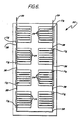
- an electrically-interconnected photovoltaic panel 50 may be assembled from a plurality of discrete, electrically-interconnected, large area photovoltaic cells.
- such panels 50 comprise a four foot long by two foot wide matrix of electrically-interconnected solar cells.
- any number of large area photovoltaic cells 10 can be electrically interconnected to form a panel 50.
- the number of large area cells 10 employed is dependent upon the power requirements of the consumer.
- the entire panel may be encapsulated in protective lamination.
- the protective lamination will assure ease of handling, durability and protection from the elements.
- the large area cells 10 are electrically connected in series by conductive strips 38, the ends 39 of which provide electrodes extending from the panel 50. These electrodes are available for electrical connection to another panel 50 or to supply power for the consumer.
Landscapes
- Photovoltaic Devices (AREA)
Description
- This invention relates generally to large area photovoltaic cells and more particularly to electrically interconnected large area photovoltaic cells. Also disclosed are the methods of producing said electrically-interconnected, large area photovoltaic cells.
- Described herein are adjacent, electrically interconnected, large area photovoltaic cells. Also discussed is the fabrication of a large area photovoltaic cell from the plurality of electrically isolated, small area segments which must be electrically-interconnected to provide an electrically operable large area solar cell and the fabrication of a plurality of adjacent, electrically-interconnected, large area solar cells from a plurality of discrete large area photovoltaic cells.
- Patents Abstracts of Japan volume 5, No. 153 (E-76), 26th September 1981 and Patents Abstracts of Japan Volume 5, No. 133 (E-71), 25th August 1981, disclose a large area photovoltaic cell comprising a plurality of small area segments sharing a common substrate and further including a plurality of semiconductor layers atop one surface of the substrate, with a transparent conductive coating atop the semiconductor layers. A plurality of busbars are connected to the small area segments and each of the busbars terminates on the same portion of the large area cell. Means are provided for electrically connecting the busbars and these means, together with the substrate, provide the output electrodes of the cell.
- Although crystal silicon devices are the basis of a huge semiconductor industry, devices made from crystal silicon have fixed parameters which are not variable as desired, require large amounts of materials, are only producible in relatively small areas and are expensive and time consuming to produce. Devices based upon amorphous silicon can eliminate these crystal silicon disadvantages. Amorphous silicon has an optical absorption edge having properties similar to a direct gap semiconductor and only a material thickness of one micrometer or less is necessary to absorb the same amount of sunlight as the 50pm thick cyrstalline silicon. Further, amorphous silicon can be made faster and more easily in larger areas than can cyrstalline silicon.
- Accordingly, a considerable effort has been made to develop processes for readily depositing amorphous semiconductor alloys or films, each of which can encompass relatively large areas, if desired, limited only by the size of the deposition equipment, and which could be readily doped to form p-type and n-type materials when p-n junction devices are to be made therefrom equivalent to those produced by their crystalline counterparts.
- Greatly improved amorphous silicon alloys having significantly reduced concentrations of localized states in the energy gaps thereof and high quality electronic properties have been prepared by glow discharge deposition as fully described in U.S. Patent No. 4,226,898, Amorphous Semiconductors Equivalent to Crystalline Semiconductors, Stanford R. Ovshinsky and Arun Madan which issued October 7, 1980, and by vapor deposition as fully described in U.S. Patent . No. 4,217,374, Stanford R. Ovshinsky and Masatsugu lzu, which issued on August 12, 1980, under the same title. As disclosed in these patents, which are incorporated herein by reference, fluorine is introduced into the amorphous silicon semiconductor to substantially reduce the density of localized states therein. It is believed that the activated fluorine readily diffuses into and bonds to the amorphous silicon in the amorphous body to substantially decrease the density of localized defect states therein, because the small size of the fluorine atoms enables them to be readily introduced into the amorphous body. The fluorine bonds to the dangling bonds of the silicon and forms what is believed to be a partially ionic stable bond with flexible bonding angles, which results in a more stable and more efficient compensation or alteration than is formed by hydrogen and other compensating or altering agents. Fluorine is considered to be a more efficient compensating or altering element than hydrogen when employed alone or with hydrogen because of its exceedingly small size, high reactivity, specificity in chemical bonding, and highest electronegativity.
- It is now known that the efficiency of a photovoltaic device may be enhanced by stacking cells atop of each other. This concept of utilizing multiple cells, to enhance photovoltaic device efficiency, was discussed at least as early as 1955 by E. D. Jackson, U.S. Patent No. 2,949,498 issued August 16, 1960. The multiple cell structures therein discussed utilized p-n junction crystalline semiconductor devices. Essentially the concept is directed to utilizing different band gap devices to more efficiently collect various portions of the solar spectrum and to increase open circuit voltage (Voc.). The tandem cell device has two or more cells with the light directed serially through each cell, with a large band gap material followed by a smaller band gap material to absorb the light passed through the first cell or layer. By substantially matching the generated currents from each cell, the overall open circuit voltage of each cell may be added, thereby producing a device which makes full use of the energy produced by incoming light.
- It is of obvious commercial importance to be able to mass produce photovoltaic devices. Unlike crystalline silicon which is limited to batch processing for the manufacture of solar cells, amorphous silicon alloys can be deposited in multiple layers over relatively large area substrates to form solar cells in a high volume, continuous processing system. Continuous processing systems of this kind are disclosed, for example, in pending patent applications: Serial No. 151,301, (Pat. No. 4400409), for A Method of Making P-Doped Silicon Films and Devices Made Therefrom; Serial No. 244 386, filed March. 16, 1981 for Continuous Systems For Depositing Amorphous Semiconductor Material; Serial No. 240,493, filed March 16, 1981 for Continuous Amorphous Solar Cell Production System; EPA No. 82108699.8, filed September 21, 1982 for Multiple Chamber Deposition and Isolation System and Method; and Serial No. 359,825, filed March 19, 1982 for Method and Apparatus for Continuously Producing Tandem Photovoltaic Cells. As disclosed in these applications, a substrate may be continuously advanced through successive triads of deposition chambers, wherein each chamber is dedicated to the deposition of a specific material. In making a solar cell of p-i-n type configuration, the first chamber of each triad is dedicated for depositing a p-type amorphous semiconductor material, the second chamber of each triad is dedicated for depositing an intrinsic semiconductor material, and the third chamber of each triad is dedicated for depositing an n-type amorphous semiconductor material.
- The resultant roll of large area photovoltaic cells manufactured by the mass production glow discharge deposition technique described hereinabove, comprises an elongated strip of substrate upon which successive semiconductor layers are deposited. It is well known that following the deposition of the semiconductor layers, a further step must be performed in order to complete fabrication of an operable, semiconductor device. In this step, a transparent, electrically conductive coating, which is characterised by high light- transmissivity and high electrical-conductivity, is deposited atop the semiconductor body. This elongated roll of photovoltaic material must now be processed to form therefrom a plurality of large area photovoltaic cells adapted for either series or parallel electrical interconnections.
- According to the present invention, there is provided a plurality of electrically interconnected large area photovoltaic cells, each cell comprising a plurality of electrically-isolated, small area segments which share a common electrically conductive substrate upon which a plurality of continuous semiconductor layers are deposited; a plurality of spaced, electrically-conductive busbars disposed atop and electrically insulated from the surface therebeneath, said busbars electrically interconnected to the small area segments of said discrete large area cells; each small area segment being defined by a discrete portion of a transparent conductive coating atop the semiconductor layers, whereby each small area segment is electrically isolated from other small area segments; and wherein each of the busbars of each large area cell terminates on the same portion of the surface of the associated large area cell; said electrically interconnected cells comprising, in combination: an electrically insulating layer applied to the busbar terminating portion of each large area cell to prevent short circuiting; first connecting means (38) for electrically connecting the busbars of each discrete large area cell; at least one means for providing electrical access to the common substrate of each large area cell from the layered surface of each large area cell; and said electrical access means and said first connecting means of adjacent large area cells being electrically interconnected to interconnect said adjacent large area cells.
- The busbars of each discrete large area cells may terminate within a peripheral border portion of that cell. Electrical access to the substrate may be provided either by electrically-conductive rivets secured within the peripheral border portion of that cell or by an exposed section of the peripheral border portion. In either event, the substrate is sufficiently accessible to provide for series or parallel electrical connection of adjacent large area cells.
- The many objects and advantages of the present invention will become clearfrom the drawings, the detailed description of the invention and the claims which follow. In the drawings:
- Figure 1 is an enlarged, fragmentary, cross- sectional view of a photovoltaic cell comprising a plurality of p-i-n type cells, each layer of the cells preferably formed of an amorphous semiconductor alloy;
- Figure 2a is a fragmentary top plan view illustrating one method of electrically interconnecting the plurality of small area segments, with grid patterns formed thereon, to provide an electrically connection, large area photovoltaic cell;
- Figure 2b is a fragmentary top plan view illustrating the electrically-isolated, small area segments of Figure 2a before the application of grid patterns thereonto;
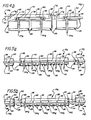
- Figure 3a is a fragmentary top plan view illustrating a first embodiment of the present invention in which an insulated metallic strip electrically interconnects adjacent large area photovoltaic cells said cells connected in series;
- Figure 3b is a fragmentary top plan view illustrating the embodiment of the present invention shown in Figure 3a as modified to provide a parallel connection of the large area cells;
- Figure 4a is a fragmentary, top plan view illustrating a second embodiment of the present invention in which an uninsulated metallic strip electrially interconnects adjacent large area photovoltaic cells, said cells connected in series;
- Figure 4b is a fragmentary top plan view illustrating the embodiment of the present invention shown in Figure 4a as modified- to provide a parallel connection of the large area cells;
- Figure 5a is a fragmentary, top plan view illustrating a third embodiment of the present invention in which an insulated metallic strip and rivets electrically interconnect adjacent large area photovoltaic cells, said cells interconnected in series;
- Figure 5b is a fragmentary, top plan view illustrating the embodiment of the present invention shown in Figure 5a as modified to provide a parallel connection of the-large area cells; and
- Figure 6 is a top plan view of a panel of photovoltaic cells formed by electrically interconnecting, in series, the adjacent large area photovoltaic cells.
- Referring now to the drawings, and particularly to Figure 1, a stacked, tandem or cascade-type, photovoltaic cell, formed of successive p-i-n layers, each layer formed from an amorphous semiconductor alloy and including an transparent, conductive coating, is shown generally by the
reference numeral 10. The methods described herein are not limited solely to the production of stacked p-i-n photovoltaic cells, but are of equal value in the production of improved Schottky or improved MIS (metal-insulator-semiconductor) type cells or simply the production of improved semiconductor devices. Regardless of cell type, the large area cells and the production techniques which are detailed in this specification find utility with photovoltaic cells formed with layers of semiconductor materials and with a transparent transparent, conductive layer deposited atop the semiconductor layers. - More particularly, Figure 1 shows a plurality of p-i-n
solar cells 12a, 12b, and 12c. Below the lowermost cell 12a, is a substrate 11 which may be a transparent conductive layer or formed from a metallic surface foil. Since certain applications may require a thin oxide layer and/or a series of base contacts prior to the application of the semiconductor material, for the purpose of this application the term substrate shall include not only a flexible film but also any elements added thereto by preliminary processing. Most commonly, the substrate 11 may be formed of stainless steel, aluminum, tantalum, molybdenum, or chrome. However, other materials may be used, including, specifically, a glass insulating base having an electrically conductive layer applied thereon. - Each of the
cells 12a, 12b and 12c include a semiconductor body containing in one embodiment, at least a silicon alloy. Each of the alloy bodies includes an n-type conductivity semiconductor orlayer 20a, 20b and 20c; anintrisic semiconductor layer 18a, 18b, and 18c; and a p-type conductivity semiconductor or layer 16a, 16b and 16c. As illustrated,cell 12b is an intermediate cell and, as indicated in Figure 1, additional intermediate cells may be stacked upon the illustrated cells. Whereas, in the preferred embodiment of the present invention, an amorphous semiconductor alloy, which includes fluorine is used to form each of the layers of the cells 12, the layers could also be formed of crystalline or polycrystalline materials, with orwithoutthe addition of fluorine. The inventive concepts disclosed herein are applicable to photovoltaic cells, regardless of materials or crystallinity. - For each of the
cells 12a, 12b and 12c, the p-type semiconductor layers 16a, 16b, 16c are ideally low light absorption, high conductivity layers. Theintrisic semiconductor layers 18a, 18b, 18c are characterized by an adjusted wavelength threshold for a solar photoresponse, high light absorption, low dark conductivity, and high photoconductivity, and include sufficient amounts of a band gap adjusting element or elements to optimize the band gap for the particular cell application. Preferably the intrisic layers are band gap adjusted to provide cell 12a with'a lowest band gap, cell 12c with the highest band gap, and cell 12bwith a band gap between the other two. The n-type layers 20a, 20b, and 20c are,,gharacterized by low light absorption, high conductivity alloy materials. The thickness of the<n-type layers is preferably in the range of about 25 to 100 angstroms (10 angstroms =inm). Thethickness of the band gap adjusted amorphous intrinsic alloy layer is preferably between about 2000 angstroms to 3,000 angstroms. The thickness of the p-type layers is preferably between 50 to 500 angstroms. Due to the shorter diffusion length of the holes, the p-type layers generally will be as thin as possible. Further, the outermost layer, here the p-type layer 20c, will be as thin as possible to avoid absorption of light and need not include the band gap adjusting element or elements. - It is to be understood that following the deposition of the semiconductor layers, a further deposition step is performed. In this step, a continuous or discontinous, transparent,
conductive layer 22 of high electrical conduction and high light transmissivity is added atop the n-type layer 20c. This transparent,conductive layer 22 may, for example, be a thin 500 angstrom thick film of indium tin oxide, (ITO), cadmium stannate (Cd 2pSn0 4µ), or doped tin oxide (Sn0 2p). Althoughgrid patterns 24 are routinely added to the transparent, conductive material, for applications involving a sufficiently small area solar cell, the transparent,conductive coating 22 is generally sufficiently conductive so agrid pattern 24 is not necessary. However, for applications such as the present one in which large area (one square foot) solar cells are fabricated, agrid pattern 24 is applied atop the transparent,conductive layer 22 to shorten the carrier path and increase the conduction efficiency thereof. This transparent,conductive layer 22, being applied directly atop the semiconductor layers, serves as a top electrode for thephotovoltaic device 10, with the conductive substrate 11 serving as a bottom electrode. Since the transparent,conductive layer 22 electrically communicates with the semiconductor layers therebelow, in the preferred embodiment, the application of a relatively thick insulating layer between the semiconductor layers and the transparent,conductive layer 22 can be used to divide the large area (one square foot) solar cell into a plurality (180) small area segments thereof for reasons which will become clear hereinafter. This method of electrical isolation is the subject of a separate patent application, entitled ISOLATION LAYER FOR PHOTOVOLTAIC DEVICE AND METHOD OF PRODUCING SAME, filed simultaneously herewith, invented by Prem Nath and Masatsugu Izu and assigned to the assignee of the instant application. That method of isolation will be further detailed in the following paragraph, only to the extent necessary to fully understand the instant disclosure. - The insulating material is applied over the surface area of the semiconductor layers so as to divide the surface thereof into a plurality of rows and columns of insulating material. When the transparent,
conductive layer 22 is subsequently deposited onto the surface of the semiconductor layers, it can only electrically communicate with those segments not covered by insulating material. Electrically-isolated, electrically-insulated, portions of semiconductor material may be thereby fabricated. - Figure 2a is a fragmentary view of the upper surface of the transparent,
conductive coating 22 applied atop the semiconductor layers of thesolar cell 10. As can be readily determined from that figure, the surface area of the semiconductor layers of thesolar cell material 10 may be divided into a plurality of electrically-isolatedsegments 26 in any one of a plurality of methods which will be described hereinafter. Although the exact number and arrangement of theisolated segments 26 of thesolar cell 10 may vary, in the preferred embodiment, twelve (12) parallel rows of fifteen (15) isolated segments 26 (a total of one hundred-eighty subcells) define the surface area of each large area (one square foot) solar cell. The term "isolated segment" is defined herein as a small surface area segment of a large area solar cell which is electrically-isolated from other segments of the surface area of the large area solar cell, but which shares a common substrate or electrode with those other segments. - The
isolated segments 26 are formed, in the preferred embodiment, by discrete portions of the , transparent,conductive coating 22 deposited atop the semiconductor layers of thesolar cell material 10. Eachisolated segment 26 may also be formed from the transparent,conductive coating 22 by other known methods such as photo- lithographing and chemical etching. For instance, a photoresist solution may be applied to the surface of the transparent,conductive coating 22 and pre-heated to dry off solvents, thus leaving a thin film as a residue. Thegrid pattern 24, one possible form of which will be described hereinafter, is then laid over the residual film, and those portions of the film not covered by the pattern are exposed to electro-magnetic radiation, typically in the ultra-violet region of the spectrum, or to a beam of electrons of appropriate energy to develop the film. During the development of the film, using conventional chemical or plasma procedures, the exposed portions (positive resist) or the unexposed portions (negative resist) of the film and the underlying transparent,conductive coating 22 are removed. The residual photoresist film is washed with a solvent to remove same from the surface of the transparent,conductive coating 22. Agrid pattern 24 may now be applied onto the surface of the now isolatedsegments 26 of the transparent,conductive coating 22. In the embodiment illustrated in Figure 2b, theisolated segments 26 of thesolar cell material 10 can be formed by dividing the transparent,conductive coating 22 into a plurality of discrete segments 22a-22u without applying a grid pattern thereonto. It is to be understood that for purposes of this description, the numeral 26 will refer to isolated segments of the transparent, conductive coating with a grid pattern applied thereonto, while the numerals 22a-22u refer to isolated segments of the transparent,conductive coating 22 not having the grid pattern applied thereonto. The discrete segments 22a-22u may be formed either by originally depositing the transparent,conductive coating 22 in a discontinuous fashion, as by the application of the insulating material as previously described, or by depositing a continuous transparent,conductive coating 22 and then removing intermediate parts by the photolithography and etching techniques previously described. Note that the electrically-insulating material may be applied atop the semiconductor layers by means of screen printing or other known techniques. - Each isolated segment, whether formed by a continuous or discontinuous transparent, conductive coating may have a
grid pattern 24 applied thereonto. The width dimension of eachgrid pattern 24 is defined by a plurality of substantially equally spaced, relatively thin, parallel, electrically-conductive lines 30 radiating perpendicularly from both sides of a tapered, relatively thick, electrically-conductive, busbar-connectingline 32 which defines the length dimension of thegrid pattern 24. The total width of eachisolated segment 26 is about three-quarters (3/4) of an inch and the total length of eachisolated segment 26 is about one (1) inch (1 inch = 2.54cm). Thegrid patterns 24 are formed are formed so as to maximize the current collected from the solar cell material while minimizing the amount of light prevented from entering the solar cell material. It should be readily apparent to one ordinarily skilled in the art that the arrangement ofisolated segments 26, the length and width dimensions of thegrid patterns 24 and theisolated segments 26, the number ofparallel lines 30, the number of parallel rows of theisolated segments 26, the total number ofisolated segments 26 formed on a large area solar cell and hence, the size and configuration of that solar cell may vary without departing from the scope of the present invention. Whatever arrangement is selected, thegrid patterns 24 may be printed, by any well known technique, such as screen printing, onto the transparent,conductive segments 26 with an electrically conductive material such as silver paste. - While two methods of forming the
isolated segments 26 of the solar cell material have been described, other well known methods of "scribing'those isolation segments are within the scope of the present invention. Moreover, when used herein, the term "scribing" is intended to encompass all such methods of removing the transparent,conductive coating 22, which include, but are not limited to: (a) chemical etching; (b) plasma etching; (c) various laser techniques; (d) a waterjet technique; or (e) applying the transparent, conductive coating with a mask to form said distinct, discontinuous segments. - If desired, each isolated segment of the
solar cell material 10 may be individually tested to determine whether the electrical output therefrom is sufficient to render it "electrically operative" or " electrically operable". As used within the context of the instant application, the terms "electrically operative isolated segment" or "electrically operable isolated segment" refer to those isolatedsegments 26 of the solar cell material which 10 provide satisfactory electrical output. The electrical connection ofisolated segments 26 of thesolar cell material 10 providing unsatisfactory electrical output reduces the overall efficiency of the solar cell material. Further, since theisolated segments 26 of large area solar cells are connected in parallel, the electrical connection of anyisolated segment 26 on a large area solar cell providing a very low voltage output could significantly decrease the electrical output of the entire large areasolar cell 10. - While it is currently necessary to divide the large area cells into small area segments due to the existence of short circuits or other defects which, if electrically-connected to operable segments, would harm or destroy the efficiency of the overall cell, it is foreseeable (especially in view of recent "short-healing" technology) that those defects can be eliminated. If the defects are eliminated, there would be no need to divide the large area cell into small area segments. Further, for certain applications (powering calculators), the size of large area cells may not be large enough to warrant further division into smaller segments. Accordingly, the electrical connections disclosed herein are not limited to large area solar cells, which include small area segments, but may also be used with undivided large area cells.
- A plurality of elongated, copper, electrically
conductive busbars 34 are affixed to the surface of the semiconductor layers with an electrically-insulating silicon adhesive. The silicon adhesive is applied as a very thin layer because thebusbars 34 are to be positioned between alternate rows ofisolated segments 26 of the solar cell material. In other words, even after thebusbars 34 are affixed to thesolar cell material 10, a lateral gap must remain between the adjacentdiscrete segments 26 of the transparent,conductive coating 26 and the associatedbusbar 34. In a preferred embodiment, wherein twelve rows ofisolated segments 26 are provided, sixconductive busbars 34, about 1/10 of an inch wide and .03 of an inch thick, are employed. The busbar-connectingline 32 from each electrically-operativeisolated segment 26 of the solar cell material is electrically-connected to anadjacent busbar 34 using a dot of electrically-conductive material such assilver paste 35. Thoseisolated segments 26 whose electrical output falls below the selected minimum satisfactory level remain electrically-isolated, by the insulating silicon adhesive, from the electrically-conductive copper busbar 34. - The foregoing sequence may be reversed and, in fact, once the incidence of electrically-operative,
isolated segments 26 routinely exceeds a predetermined level, the testing step may be omitted. In such cases, it is actually desirable to reverse the sequence and adhesively secure thecopper busbars 34 to the surface of transparent,conductive coating 22 prior to printing thegrid patterns 24 onto theisolated segments 26. This reversed sequence is preferable because thegrid patterns 24 and the electrical connections thereof to thecopper busbars 34 may be simultaneously accomplished. Although the sequence is not important from an operational standpoint, it is significant from an assembly line standpoint where the elimination of a step can represent important economic gains. - Figures 3a, 3b, 4a, 4b, 5a and 5b are fragmentary views illustrating the top surface of adjacent large area
photovoltaic cells 10 and specifically showing the manner in which said large area cells are electrically interconnected pursuant to the teachings of this invention. More particularly, depicted therein are portions of electrically interconnected large area photovoltaic cells such as 10a and 10b, and in the case of Figures 5a and 5b, cell 10c. Although different methods of connecting these large area cells are shown in the Figures, the same reference numeral:will depict common elements in each of the embodiments. It is to be understood that each of thephotovoltaic cells 10 are preferably formed of a plurality of electrically isolated, small area segments which will be generally referred to by thereference numeral 26. Although each electrically-isolatedsegment 26 is capable of functioning as a photovoltaic device independent of everyother segment 26, the present invention deals with the electrical interconnection of (1) these electrically-isolatedsegments 26 to obtain an overall electrical output from the large areasolar cell 10 which is the sum of the output of eachisolated segment 26, and (2) adjacent large area solar cells, such as 10a and 10b, to obtain an electrical output which is the sum of the output of each electrically-interconnected large area cell, such as 10a and 10b. - Note that in Figure 3a, electrically inoperative segments of the large area photovoltaic cells 10a and 10b are not connected to the
busbars 34a, 34b and 34c but rather, they are left electrically isolated. Specifically, in cell 10b, segments 26a and 26b are electrically inoperative and consequently have not been connected to busbar 34c. Note further that, while Figures 3a, 3b, 4a and 4b illustrate only twobusbars 34a and 34b connecting the electrically-isolatedsegments 26 of large area solar cell 10a, this is merely for convenience in understanding and economy of space in this description. In the actual practice of the invention, cell 10a would be composed of a greater number (180) of electrically-isolated segments linked by a greater number (6) of thebusbars 34. These six busbars 34a-34f are shown in the embodiment of Figures 5a and 5b. - As can be seen from the preferred embodiments illustrated in each of the Figures 3a-5b, the end of each of the
copper busbars 34 extends beyond the periphery of the active area of each large area photovoltaic cell and terminates on an upperperipheral border portion 36. For purposes of this disclosure, (1) "active area" is defined as that portion of the large areaphotovoltaic cell 10 which includes electrically communicating substrate, semiconductor and transparent, conductive coating layers, and (2) the "same portion" of thelarge area cell 10 is defined as any continuous segment of the surface of the cell without regard to shape or size. An electrically-insulating layer of any well known type must be applied below thebusbars 34 on theborder portion 36 to be sure that (1) said portion (36) is electrically "inactive", and (2) thebusbars 34 do not electrically contact and consequently short circuit current to the substrate 11. The electrically-insulating layer may be applied in any well known manner, such as by depositing an insulating coating simultaneously with the application of the electrically-insulating material which forms the electrically-isolated small area segments of each of thelarge area cells 10. - Having electrically interconnected the electrically-operable, electrically-isolated
segments 26 of the large area photovoltaic cells 10a and 10b, to thebusbars 34a, 34b and 34c, respectively, and having electrically insulated those busbars from the substrate 11 on the electrically insulatedperipheral border portion 36 of the cells 10a and 10b, it is necessary to electrically interconnect the busbars of each large area cell in order to provide a single electrode therefrom. The lower or base electrode of each large area photovoltaic cell such as, 10a and 10b, is provided by the common substrate 11. - More specifically, the electrically-isolated
segments 26 of the large area cell 10a share a common base electrode or substrate 11. For convenience of electrical interconnection and commercial production, in the first and second preferred embodiments illustrated in Figures 3a, 3b, 4a and 4b, a section 11 a of the upper left hand corner of the upperperipheral border portion 36 of the large area photovoltaic cell 10a is exposed and is therefor adapted to provide electrical access to the common substrate 11. In Figures 3b and 4b, two distal sections 11a of theperipheral border portion 36 are exposed to provide electrical access to the common substrate 11. The exposed substrate sections 11 a may be formed by burnishing the previously deposited semiconductor layers, or they may be formed by masking a portion of the peripheral border during the deposition of semiconductor layers, or by etching those semiconductor layers from the substrate, or by any other commonly employed technique. Note that electrical access to the substrate is provided in Figures 5a and 5b by plated copper rivets 48. The copper rivets preferably include surrated washers for establishing good electrical contact with the substrate 11. Onesuch rivet 48 is secured to each large area cell 10a, 10b and 10c for the series connection shown in Figure 5a, while tworivets 48 are secured to the large area cells 10a, 10b and 10c for the parallel connection shown in Figure 5b. - Electrical interconnection of the
busbars 34a and 34b of large area cell 10a is accomplished, in the first embodiment of Figures 3a and 3b, by a means of an electrically-insulated, conductivemetallic strip 38. In its most preferred form, this strip comprises an inner metallic core made of an electrically-conductive material such as nickel- plated copper, protected by a surrounding, electrically-insulating jacket such as glass-filled teflon, polyvinylcholoride, vinylacetate, or other like flexible, dielectric material. The advantage of the insulating jacket is the added security it provides against the possibility of short circuiting. - In the embodiment of Figures 3a and 3b, a length of the
conductive strip 38 is electrically connected to thebusbars 34 by punching holes through thestrip 38 at positions, which, when the strip is applied atop theperipheral border portion 36 of the large area cell 10a, will present the metallic core thereof to eachbusbar 34a and 34b. In other words, the holes in theconductive strip 38 are formed to directly overlie eachbusbar 34 of eachlarge area cell 10. Thestrip 38 is then securely electrically connected to each of the busbars, 34a and 34b, on that large area cell, such as 10a, by means of asolder joint 40. In an identical manner, the busbars, such as 34c of large area cell 10b, are electrically interconnected by a length ofconductive strip 38. In an alternative embodiment, the portion of the insulating jacket of thestrip 38 immediately overlying each of the busbars may be stripped away and the exposed, conductive core thereof directly fastened, as by soldering, to the busbars. - Moving now to the embodiment viewed in Figure 3b, regardless of the manner in which the conductive core of the
metallic strip 38 is exposed, electrically-conductivemetallic wires 42 may be soldered, as at 44, to each of the ends of thosestrips 38, the conductive core having first been exposed at said ends. Similarly, themetallic wires 42 may be electrically connected, as byweld joints 45, to the exposed sections 11 a of substrate 11. In this manner, the adjacent large area cells 10a and 10b shown in Figure 3b are adapted for parallel interconnection. The parallel connection will be further described in a later paragraph. - In the second preferred embodiment, shown in Figures 4a and 4b, electrical interconnection of the
busbars 34a and 34b of the large area solar cell 10a is accomplished by means of an electrically-conductive, uninsulatedmetallic strip 38. While thisstrip 38 is readily connected to thebusbars 34a and 34b by soldering, a thin electrically-insulatingtape 42 must first be placed onto theperipheral border portion 36 to insure that the uninsulated surface of theconductive strip 38 does not short circuit current to the substrate 11. - As with the embodiment of Figure 3b, Figure 4b shows electrically-conductive,
metallic wires 42 soldered, as at 44, to each end of thestrips 38. Similarly, themetallic wires 42 are welded to the exposed sections 11a of substrate 11. In this manner, the adjacent large area photovoltaic cells 10a and 10b shown in Figure 4b are adapted for parallel interconnection. This parallel interconnection will be detailed in a later paragraph. - Referring now to Figures 5a and 5b, a still further embodiment of the present invention is illustrated. In this embodiment, electrical interconnection of the busbars 34a-34f of the large area solar cell 10a is accomplished by means of an electrically-insulated, electrically-conductive,
metal strip 38. Thestrip 38, as previously described with reference to the embodiment of Figures 3a and 3b, includes a metallic core made of an electrically-conductive material such as copper, protected by a surrounding, electrically-insulating jacket such as Teflon, etc. However, unlike the embodiment disclosed with respect to Figures 3a and 3b, electrical access to the substrate 11 is provided by at least one platedcopper rivet 48 which is secured, within theperipheral border portion 36, to eachlarge area cell 10. Only onerivet 48 need be secured to thelarge area cell 10 for series connection of adjacentlarge area cells 10, while two rivets are secured for the parallel interconnection thereof. - A length of the
conductive strip 38 is electrically connected to the busbars 34a-34f of large area cell 10a by punching holes through thestrip 38. More particularly, the holes are punched at positions, which, when the strip is applied atop theperipheral border portion 36 of the large area cell 10a will present the metallic core thereof to said busbars 34a-34f. Thestrip 38 is then securely electrically connected to the busbars by means of asolder joint 44. In an identical manner, thebusbars 34 of the adjacent large area cells 10b and 10c are electrically interconnected by a length ofonductive strip 38. In an alternate embodiment, the portion of the insulating jacket of thestrip 38 immediately overlying each of the busbars may be stripped away and the exposed, conductive core thereof soldered directly to the busbars. - For purposes of providing parallel electrical interconnections, between the adjacent large area cells 10a, 10b and 10c, electrically conductive
metallic wires 42 may be soldered, as at 44, to each of the ends of theconductive strips 38, the conductive core having first been exposed at said ends. Similarly, themetallic wires 42 may be electrically connected to the opposed copper plated rivets, see Figure 5b. - While not shown, it should be readily apparent that the
rivets 48 could be replaced by exposed sections 11a of the substrate 11 to which themetallic wires 42 would be welded without departing from the scope of the instant invention. - The electrically-interconnected large area
photovoltaic cell 10 is thereby provided with (1) a first electrode in the form of one or more of the exposed portions 11a a of the substrate 11, or one or moreconductive rivets 48, and (2) a second electrode formed by the electrically-conductive tape 38 which electrically-interconnects the plurality ofcopper busbars 34, which in turn, electrically connect the plurality of isolatedsmall area segments 26 of eachlarge area cell 10. - In order to electrically interconnect adjacent large area photovoltaic cells, it is necessary to electrically interconnect the electrodes extending from said adjacent cells. This interconnection may be advantageously accomplished by means of an elongated piece of the electrically-
conductive strip 38 discussed hereinabove. In those instances in which thestrip 38 interconnects discrete large area photovoltaic cells, it is preferred, but by no means essential, that the strip be electrically insulated to prevent shorting as thestrip 38 passes over theedges 42 between those adjacentlarge area cells 10. - More particularly and referring specifically to the embodiments illustrated in Figures 3a, 4a and 5a, electrical interconnection of one large area photovoltaic cell 10a to an adjacent large area photovoltaic cell 10b (and in the case of Figure 5a, also to cell 10c) is preferably accomplished in a series mode by fastening the conductive strip 38a, which electrically interconnects the
busbars 34a and 34b of said large area cell 10a, to the substrate electrode of the adjacent large area cell 10b. The substrate electrode is either the exposed section 11a of the substrate 11, as in the embodiment of Figures 3a and 4a, or the platedrivet 48 as in the embodiment of Figure 5a. Since the substrate is formed from stainless steel, theconductive strip 38 must be spot welded to the exposed section 11 a thereof, when the exposed substrate embodiment is employed. Note, however, that if the substrate is plated, soldering methods may be employed. Theconductive strip 38 is fastened to the substrate 11 by means of the platedrivet 48 in those instances in which the photovoltaic cell is likely to receive an extensive amount of abuse. Of course, when the plated rivet is used, the exposed head thereof should be leveled, by filing or sanding, so as to present a smooth exterior profile and thereby eliminate bubble and stress formation which would otherwise occur during the encapsulation process. - Turning now to the embodiments illustrated in Figures 3b, 4b and 5b, the parallel interconnection of one large area photovoltaic cell 10a to an adjacent large area photovoltaic cell 10b is depicted. In the embodiment illustrated by Figure 5b, the large area photovoltaic cell 10a is shown electrically interconnected in parallel to the adjacent large area photovoltaic cells 10b and 10c.
- The parallel interconnection of the Figures 3b, 4b and 5a embodiments are substantially identical. The only differences are that (1) the electrically-insulating layer, Figure 4b embodiment, is applied along the
peripheral border portion 36 of eachlarge area cell 10 prior to electrically connecting the uninsulated,conductive strip 38 to thebusbars 34, and (2) the metallic wire leads 42 are secured to the platedcopper rivets 48 in the Figure 5b embodiment, rather than to the exposed section of the substrate 11 as in the Figure 3b and 4b embodiments. Once theconductive strips 38 and the metallic wire leads 42 have been electrically connected to the discretelarge area cells 10, the electrical parallel interconnection of adjacent ones of those cells is identical regardless of the embodiment. - More particularly, the parallel interconnection is accomplished by electrically joining, by solder or solderless connection, the metallic wire lead 42 from the substrate and from the
conductive strip 38 of one large area cell, such as 10a, to the metallic wire lead 42 from the substrate and from theconductive strip 38 of the adjacent large area cell, such as 10b. Note that it is necessary to use two wire leads 42 from each side of thelarge area cell 10 if that large area cell has been or will be encapsulated prior to electrical interconnection with an adjacent large area cell. In those instances in which the large area cells are to be encapsulated by protective coverings after electrical interconnection, each of the adjacentlarge area cells 10 need only be provided with one of the two requisite wire leads 42. More particularly and viewing Figure 3b, large area cell 10a may be provided with thewire lead 42 connected to theconductive strip 38 and large area cell 10b may be provided with thewire lead 42 connected to the exposed section 11 a of the substrate 11. The electrical interconnection of the large area cells 10a and 10b is accomplished by (1) soldering the wire lead from the conductive strip of cell 10a to the conductive strip of cell 10b, and (2) welding the wire lead from the exposed substrate section 11a of cell 10b to the exposed substrate section 11 a of the cell 10a. The adjacent, electrically-interconnected large area cells 10a and 10b may now be encapsulated. - . Note that, although, wire leads 42 are shown and described as electrically interconnecting adjacent
conductive strips 38 of adjacentlarge area cells 10, the electrical interconnection between thebusbars 34 of adjacentlarge area cells 10 could be accomplished by a single, continuous length of the electrically-conductive strip 38 without departing from the spirit or scope of the invention. - Utilizing the techniques detailed hereinabove, an electrically-interconnected photovoltaic panel 50 may be assembled from a plurality of discrete, electrically-interconnected, large area photovoltaic cells. Typically, such panels 50 comprise a four foot long by two foot wide matrix of electrically-interconnected solar cells.
- Obviously, any number of large area
photovoltaic cells 10 can be electrically interconnected to form a panel 50. The number oflarge area cells 10 employed is dependent upon the power requirements of the consumer. Once the preselected number ofphotovoltaic cells 10 are electrically interconnected to form a photovoltaic panel 50 adapted to supply a given amount of power, the entire panel may be encapsulated in protective lamination. The protective lamination will assure ease of handling, durability and protection from the elements. Regardless of the encapsulating process which is employed, it is preferred that thelarge area cells 10 are electrically connected in series byconductive strips 38, the ends 39 of which provide electrodes extending from the panel 50. These electrodes are available for electrical connection to another panel 50 or to supply power for the consumer. - It should be understood that the present invention is not limited to the precise structure of the illustrated embodiments. It is intended that the foregoing description of the presently preferred embodiment be regarded as an illustration rather than as a limitation of the present invention. It is the following claims, including all equivalents which are intended to define the scope of the invention.
Claims (7)
Applications Claiming Priority (2)
| Application Number | Priority Date | Filing Date | Title |
|---|---|---|---|
| US440385 | 1982-11-09 | ||
| US06/440,385 US4443652A (en) | 1982-11-09 | 1982-11-09 | Electrically interconnected large area photovoltaic cells and method of producing said cells |
Publications (3)
| Publication Number | Publication Date |
|---|---|
| EP0112028A2 EP0112028A2 (en) | 1984-06-27 |
| EP0112028A3 EP0112028A3 (en) | 1985-08-07 |
| EP0112028B1 true EP0112028B1 (en) | 1989-12-27 |
Family
ID=23748552
Family Applications (1)
| Application Number | Title | Priority Date | Filing Date |
|---|---|---|---|
| EP83306832A Expired EP0112028B1 (en) | 1982-11-09 | 1983-11-09 | Electrically connected and electrically interconnected large area photovoltaic cells and method of producing said cells |
Country Status (6)
| Country | Link |
|---|---|
| US (1) | US4443652A (en) |
| EP (1) | EP0112028B1 (en) |
| JP (1) | JPS5999779A (en) |
| KR (1) | KR910006676B1 (en) |
| CA (1) | CA1192292A (en) |
| DE (1) | DE3381035D1 (en) |
Families Citing this family (64)
| Publication number | Priority date | Publication date | Assignee | Title |
|---|---|---|---|---|
| JPS6080272A (en) * | 1983-10-07 | 1985-05-08 | Canon Inc | Charge transfer element |
| US4514583A (en) * | 1983-11-07 | 1985-04-30 | Energy Conversion Devices, Inc. | Substrate for photovoltaic devices |
| US4590327A (en) * | 1984-09-24 | 1986-05-20 | Energy Conversion Devices, Inc. | Photovoltaic device and method |
| US4574160A (en) * | 1984-09-28 | 1986-03-04 | The Standard Oil Company | Flexible, rollable photovoltaic cell module |
| GB2177254B (en) * | 1985-07-05 | 1988-09-01 | Stc Plc | Testing integrated circuits |
| JPH0744286B2 (en) * | 1986-03-04 | 1995-05-15 | 三菱電機株式会社 | Method for manufacturing amorphous photovoltaic module |
| US4773944A (en) * | 1987-09-08 | 1988-09-27 | Energy Conversion Devices, Inc. | Large area, low voltage, high current photovoltaic modules and method of fabricating same |
| JPH0644114Y2 (en) * | 1988-03-31 | 1994-11-14 | 日本電気株式会社 | Solar cell panel substrate |
| CA2024662A1 (en) * | 1989-09-08 | 1991-03-09 | Robert Oswald | Monolithic series and parallel connected photovoltaic module |
| US5164020A (en) * | 1991-05-24 | 1992-11-17 | Solarex Corporation | Solar panel |
| WO1994022172A1 (en) * | 1993-03-24 | 1994-09-29 | E.I. Du Pont De Nemours And Company | Solar panels and process for manufacture thereof |
| JP3099604B2 (en) * | 1993-09-28 | 2000-10-16 | 富士電機株式会社 | Flexible photoelectric conversion module, its connection method and its manufacturing apparatus |
| US5863354A (en) * | 1993-09-28 | 1999-01-26 | Fuji Electric Co., Ltd. | Flexible photoelectric conversion module |
| DE69534582T2 (en) * | 1994-05-19 | 2006-07-20 | Canon K.K. | Photovoltaic device, electrode structure thereof and manufacturing method |
| US5457057A (en) * | 1994-06-28 | 1995-10-10 | United Solar Systems Corporation | Photovoltaic module fabrication process |
| US5517956A (en) * | 1994-08-11 | 1996-05-21 | Del West Engineering, Inc. | Titanium engine valve |
| GB9420511D0 (en) * | 1994-10-11 | 1994-11-23 | Ici Plc | High voltage generator |
| JP3352252B2 (en) * | 1994-11-04 | 2002-12-03 | キヤノン株式会社 | Solar cell element group, solar cell module and method of manufacturing the same |
| US7075002B1 (en) * | 1995-03-27 | 2006-07-11 | Semiconductor Energy Laboratory Company, Ltd. | Thin-film photoelectric conversion device and a method of manufacturing the same |
| DE19617220A1 (en) * | 1996-04-30 | 1997-11-06 | Julian Dipl Ing Schueren | Solar generator |
| DE19711319C1 (en) * | 1997-03-18 | 1998-03-12 | Daimler Benz Aerospace Ag | Solar module for space satellite |
| US8664030B2 (en) | 1999-03-30 | 2014-03-04 | Daniel Luch | Collector grid and interconnect structures for photovoltaic arrays and modules |
| US20090293941A1 (en) * | 2008-06-02 | 2009-12-03 | Daniel Luch | Photovoltaic power farm structure and installation |
| DE10020784A1 (en) * | 2000-04-28 | 2001-11-08 | Ist Inst Fuer Solartechnologie | Photovoltaic module and method for its production |
| JP4526223B2 (en) * | 2001-06-29 | 2010-08-18 | シャープ株式会社 | Wiring member, solar cell module and manufacturing method thereof |
| AU2003902270A0 (en) * | 2003-05-09 | 2003-05-29 | Origin Energy Solar Pty Ltd | Separating and assembling semiconductor strips |
| DE102004021570B4 (en) * | 2003-06-25 | 2013-10-10 | Hts - Hoch Technologie Systeme Gmbh | Arrangement for fastening and / or contacting flexible solar cells on printed circuit boards |
| JP4368151B2 (en) * | 2003-06-27 | 2009-11-18 | 三洋電機株式会社 | Solar cell module |
| US7687234B2 (en) * | 2003-12-15 | 2010-03-30 | Geneohm Sciences, Inc. | Carbon electrode surface for attachment of DNA and protein molecules |
| US20050224109A1 (en) * | 2004-04-09 | 2005-10-13 | Posbic Jean P | Enhanced function photovoltaic modules |
| JP2007222907A (en) * | 2006-02-23 | 2007-09-06 | Denso Corp | Laser irradiation soldering method for wiring members |
| US8884155B2 (en) | 2006-04-13 | 2014-11-11 | Daniel Luch | Collector grid and interconnect structures for photovoltaic arrays and modules |
| US9006563B2 (en) | 2006-04-13 | 2015-04-14 | Solannex, Inc. | Collector grid and interconnect structures for photovoltaic arrays and modules |
| US8822810B2 (en) | 2006-04-13 | 2014-09-02 | Daniel Luch | Collector grid and interconnect structures for photovoltaic arrays and modules |
| US9865758B2 (en) | 2006-04-13 | 2018-01-09 | Daniel Luch | Collector grid and interconnect structures for photovoltaic arrays and modules |
| US8729385B2 (en) | 2006-04-13 | 2014-05-20 | Daniel Luch | Collector grid and interconnect structures for photovoltaic arrays and modules |
| US9236512B2 (en) | 2006-04-13 | 2016-01-12 | Daniel Luch | Collector grid and interconnect structures for photovoltaic arrays and modules |
| US20080011347A1 (en) * | 2006-07-14 | 2008-01-17 | Hitachi Cable, Ltd. | Connecting lead wire for a solar battery module, method for fabricating same, and solar battery module using the connecting lead wire |
| US20080216887A1 (en) * | 2006-12-22 | 2008-09-11 | Advent Solar, Inc. | Interconnect Technologies for Back Contact Solar Cells and Modules |
| WO2008093108A1 (en) * | 2007-02-02 | 2008-08-07 | G24 Innovations Limited | Web transport |
| US20090104342A1 (en) * | 2007-10-22 | 2009-04-23 | Applied Materials, Inc. | Photovoltaic fabrication process monitoring and control using diagnostic devices |
| US20090102502A1 (en) * | 2007-10-22 | 2009-04-23 | Michel Ranjit Frei | Process testers and testing methodology for thin-film photovoltaic devices |
| CN100559614C (en) * | 2008-08-28 | 2009-11-11 | 苏州富能技术有限公司 | Thin film solar cell module and processing method thereof |
| JP2010103510A (en) * | 2008-09-29 | 2010-05-06 | Semiconductor Energy Lab Co Ltd | Photoelectric conversion device and method of manufacturing the same |
| FR2945670B1 (en) * | 2009-05-15 | 2011-07-15 | Total Sa | PHOTOVOLTAIC DEVICE AND METHOD OF MANUFACTURE |
| JP5174972B2 (en) * | 2009-11-05 | 2013-04-03 | 三菱電機株式会社 | Thin film solar cell module and manufacturing method thereof |
| US20110240337A1 (en) * | 2010-04-05 | 2011-10-06 | John Montello | Interconnects for photovoltaic panels |
| JP2012222046A (en) * | 2011-04-05 | 2012-11-12 | Mitsui Mining & Smelting Co Ltd | Electrode sheet for organic device, organic device module, and method of manufacturing the same |
| US9698284B2 (en) * | 2011-08-31 | 2017-07-04 | Alta Devices, Inc. | Individual finger isolation through spot application of a dielectric in an optoelectronic device |
| US8846417B2 (en) * | 2011-08-31 | 2014-09-30 | Alta Devices, Inc. | Device and method for individual finger isolation in an optoelectronic device |
| EP2786421A4 (en) * | 2011-11-30 | 2017-06-07 | Corsam Technologies LLC | Multi-junction photovoltaic modules incorporating ultra-thin flexible glass |
| US20140069479A1 (en) * | 2012-09-11 | 2014-03-13 | Samsung Sdi Co., Ltd. | Photoelectric Device Module and Manufacturing Method Thereof |
| US8916038B2 (en) * | 2013-03-13 | 2014-12-23 | Gtat Corporation | Free-standing metallic article for semiconductors |
| US8936709B2 (en) | 2013-03-13 | 2015-01-20 | Gtat Corporation | Adaptable free-standing metallic article for semiconductors |
| CN105162407B (en) * | 2014-06-20 | 2018-02-02 | 维斯幕达有限公司 | For the apparatus and system for the photovoltaic panel for connecting and pre-fixing before and after self-leveling assembled battery piece |
| JP2016039198A (en) * | 2014-08-06 | 2016-03-22 | セイコーエプソン株式会社 | Solar battery, electronic apparatus and method of manufacturing solar battery |
| USD896747S1 (en) * | 2014-10-15 | 2020-09-22 | Sunpower Corporation | Solar panel |
| US10941612B2 (en) * | 2015-02-24 | 2021-03-09 | Lutron Technology Company Llc | Photovoltaic cells arranged in a pattern |
| EP3652790B1 (en) * | 2017-07-14 | 2023-10-04 | Commonwealth Scientific and Industrial Research Organisation | Photovoltaic apparatus and method |
| DE102018116466B3 (en) * | 2018-07-06 | 2019-06-19 | Solibro Hi-Tech Gmbh | Thin-film solar module and method for producing a thin-film solar module |
| US10892461B2 (en) * | 2018-08-31 | 2021-01-12 | Shanghai Vekan Precision Industry Co., Ltd. | Busbar with insulation coating for new energy automobile |
| US10822503B2 (en) * | 2018-08-31 | 2020-11-03 | Shanghai Vekan Precision Industry Co., Ltd | Processing technology of busbar for new energy automobile |
| DE102019122213A1 (en) * | 2019-08-19 | 2021-02-25 | Heliatek Gmbh | Method for electrically conductive contacting of an optoelectronic component having at least one protective layer and optoelectronic component with such contacting |
| CN115148827A (en) * | 2021-03-30 | 2022-10-04 | 金阳(泉州)新能源科技有限公司 | Welding method for back contact solar cell chip solder strip |
Family Cites Families (8)
| Publication number | Priority date | Publication date | Assignee | Title |
|---|---|---|---|---|
| US2820841A (en) * | 1956-05-10 | 1958-01-21 | Clevite Corp | Photovoltaic cells and methods of fabricating same |
| US4140545A (en) * | 1975-12-18 | 1979-02-20 | Sharp Kabushiki Kaisha | Plural solar cell arrangement including transparent interconnectors |
| US4089576A (en) * | 1976-12-20 | 1978-05-16 | General Electric Company | Insulated connection of photovoltaic devices |
| DE2944185A1 (en) * | 1979-11-02 | 1981-05-07 | Licentia Patent-Verwaltungs-Gmbh, 6000 Frankfurt | SOLAR CELL |
| JPS5946426B2 (en) * | 1979-11-13 | 1984-11-12 | 富士電機株式会社 | How to manufacture solar cells |
| JPS5943102B2 (en) * | 1979-12-14 | 1984-10-19 | 富士電機株式会社 | solar cells |
| US4400409A (en) * | 1980-05-19 | 1983-08-23 | Energy Conversion Devices, Inc. | Method of making p-doped silicon films |
| US4419530A (en) * | 1982-02-11 | 1983-12-06 | Energy Conversion Devices, Inc. | Solar cell and method for producing same |
-
1982
- 1982-11-09 US US06/440,385 patent/US4443652A/en not_active Expired - Lifetime
-
1983
- 1983-11-08 JP JP58209769A patent/JPS5999779A/en active Granted
- 1983-11-08 CA CA000440725A patent/CA1192292A/en not_active Expired
- 1983-11-09 KR KR1019830005316A patent/KR910006676B1/en not_active Expired
- 1983-11-09 EP EP83306832A patent/EP0112028B1/en not_active Expired
- 1983-11-09 DE DE8383306832T patent/DE3381035D1/en not_active Expired - Fee Related
Also Published As
| Publication number | Publication date |
|---|---|
| JPS5999779A (en) | 1984-06-08 |
| KR910006676B1 (en) | 1991-08-30 |
| KR850003481A (en) | 1985-06-17 |
| EP0112028A2 (en) | 1984-06-27 |
| CA1192292A (en) | 1985-08-20 |
| DE3381035D1 (en) | 1990-02-01 |
| EP0112028A3 (en) | 1985-08-07 |
| JPH0554276B2 (en) | 1993-08-12 |
| US4443652A (en) | 1984-04-17 |
Similar Documents
| Publication | Publication Date | Title |
|---|---|---|
| US4443652A (en) | Electrically interconnected large area photovoltaic cells and method of producing said cells | |
| EP0112029B1 (en) | Isolation layer for photovoltaic device and method of producing same | |
| US4783421A (en) | Method for manufacturing electrical contacts for a thin-film semiconductor device | |
| US4542255A (en) | Gridded thin film solar cell | |
| US5268037A (en) | Monolithic, parallel connected photovoltaic array and method for its manufacture | |
| US6011215A (en) | Point contact photovoltaic module and method for its manufacture | |
| US7498508B2 (en) | High voltage solar cell and solar cell module | |
| US5468988A (en) | Large area, through-hole, parallel-connected photovoltaic device | |
| US3411952A (en) | Photovoltaic cell and solar cell panel | |
| US5580509A (en) | Method for electrically contacting thin-film solar modules | |
| US4726849A (en) | Photovoltaic device and a method of manufacturing thereof | |
| US4419530A (en) | Solar cell and method for producing same | |
| KR100334595B1 (en) | Manufacturing method of photovoltaic device | |
| US4808242A (en) | Photovoltaic device and a method of manufacturing thereof | |
| US4854974A (en) | Electrical contacts for a thin-film semiconductor device | |
| JP3613851B2 (en) | Integrated thin film solar cell | |
| JPH04276665A (en) | integrated solar cells | |
| US11646387B2 (en) | Laser assisted metallization process for solar cell circuit formation | |
| JPS60240171A (en) | Solar electric generator | |
| KR20200130495A (en) | Laser-assisted metallization process for solar cell stringing | |
| JP2855299B2 (en) | Solar cell module | |
| JPS6357952B2 (en) | ||
| JPS6357953B2 (en) | ||
| JPH0415631B2 (en) | ||
| JPH06120533A (en) | Thin film solar cell and method of manufacturing the same |
Legal Events
| Date | Code | Title | Description |
|---|---|---|---|
| PUAI | Public reference made under article 153(3) epc to a published international application that has entered the european phase |
Free format text: ORIGINAL CODE: 0009012 |
|
| AK | Designated contracting states |
Designated state(s): BE CH DE FR GB IT LI NL |
|
| PUAL | Search report despatched |
Free format text: ORIGINAL CODE: 0009013 |
|
| AK | Designated contracting states |
Designated state(s): BE CH DE FR GB IT LI NL |
|
| 17P | Request for examination filed |
Effective date: 19850926 |
|
| 17Q | First examination report despatched |
Effective date: 19870330 |
|
| GRAA | (expected) grant |
Free format text: ORIGINAL CODE: 0009210 |
|
| AK | Designated contracting states |
Kind code of ref document: B1 Designated state(s): BE CH DE FR GB IT LI NL |
|
| PG25 | Lapsed in a contracting state [announced via postgrant information from national office to epo] |
Ref country code: NL Effective date: 19891227 Ref country code: LI Effective date: 19891227 Ref country code: IT Free format text: LAPSE BECAUSE OF FAILURE TO SUBMIT A TRANSLATION OF THE DESCRIPTION OR TO PAY THE FEE WITHIN THE PRESCRIBED TIME-LIMIT;WARNING: LAPSES OF ITALIAN PATENTS WITH EFFECTIVE DATE BEFORE 2007 MAY HAVE OCCURRED AT ANY TIME BEFORE 2007. THE CORRECT EFFECTIVE DATE MAY BE DIFFERENT FROM THE ONE RECORDED. Effective date: 19891227 Ref country code: CH Effective date: 19891227 Ref country code: BE Effective date: 19891227 |
|
| REF | Corresponds to: |
Ref document number: 3381035 Country of ref document: DE Date of ref document: 19900201 |
|
| ET | Fr: translation filed | ||
| REG | Reference to a national code |
Ref country code: CH Ref legal event code: PL |
|
| NLV1 | Nl: lapsed or annulled due to failure to fulfill the requirements of art. 29p and 29m of the patents act | ||
| PLBE | No opposition filed within time limit |
Free format text: ORIGINAL CODE: 0009261 |
|
| STAA | Information on the status of an ep patent application or granted ep patent |
Free format text: STATUS: NO OPPOSITION FILED WITHIN TIME LIMIT |
|
| 26N | No opposition filed | ||
| PGFP | Annual fee paid to national office [announced via postgrant information from national office to epo] |
Ref country code: GB Payment date: 20001004 Year of fee payment: 18 |
|
| PGFP | Annual fee paid to national office [announced via postgrant information from national office to epo] |
Ref country code: FR Payment date: 20001107 Year of fee payment: 18 |
|
| PGFP | Annual fee paid to national office [announced via postgrant information from national office to epo] |
Ref country code: DE Payment date: 20001124 Year of fee payment: 18 |
|
| PG25 | Lapsed in a contracting state [announced via postgrant information from national office to epo] |
Ref country code: GB Free format text: LAPSE BECAUSE OF NON-PAYMENT OF DUE FEES Effective date: 20011109 |
|
| REG | Reference to a national code |
Ref country code: GB Ref legal event code: IF02 |
|
| GBPC | Gb: european patent ceased through non-payment of renewal fee |
Effective date: 20011109 |
|
| PG25 | Lapsed in a contracting state [announced via postgrant information from national office to epo] |
Ref country code: DE Free format text: LAPSE BECAUSE OF NON-PAYMENT OF DUE FEES Effective date: 20020702 |
|
| PG25 | Lapsed in a contracting state [announced via postgrant information from national office to epo] |
Ref country code: FR Free format text: LAPSE BECAUSE OF NON-PAYMENT OF DUE FEES Effective date: 20020730 |
|
| REG | Reference to a national code |
Ref country code: FR Ref legal event code: ST |
|
| REG | Reference to a national code |
Ref country code: FR Ref legal event code: ST |