EP0110283B1 - Storage target for storage tubes and method of fabrication - Google Patents
Storage target for storage tubes and method of fabrication Download PDFInfo
- Publication number
- EP0110283B1 EP0110283B1 EP83111622A EP83111622A EP0110283B1 EP 0110283 B1 EP0110283 B1 EP 0110283B1 EP 83111622 A EP83111622 A EP 83111622A EP 83111622 A EP83111622 A EP 83111622A EP 0110283 B1 EP0110283 B1 EP 0110283B1
- Authority
- EP
- European Patent Office
- Prior art keywords
- storage
- collector electrode
- substrate
- target
- stripes
- Prior art date
- Legal status (The legal status is an assumption and is not a legal conclusion. Google has not performed a legal analysis and makes no representation as to the accuracy of the status listed.)
- Expired
Links
- 238000003860 storage Methods 0.000 title claims description 157
- 238000004519 manufacturing process Methods 0.000 title claims description 6
- 239000000758 substrate Substances 0.000 claims description 58
- 239000013078 crystal Substances 0.000 claims description 28
- 229910052594 sapphire Inorganic materials 0.000 claims description 28
- 239000010980 sapphire Substances 0.000 claims description 28
- 238000010894 electron beam technology Methods 0.000 claims description 12
- VYZAMTAEIAYCRO-UHFFFAOYSA-N Chromium Chemical compound [Cr] VYZAMTAEIAYCRO-UHFFFAOYSA-N 0.000 description 4
- 229910052804 chromium Inorganic materials 0.000 description 4
- 239000011651 chromium Substances 0.000 description 4
- 238000010276 construction Methods 0.000 description 4
- 238000012986 modification Methods 0.000 description 4
- 230000004048 modification Effects 0.000 description 4
- PNEYBMLMFCGWSK-UHFFFAOYSA-N Alumina Chemical compound [O-2].[O-2].[O-2].[Al+3].[Al+3] PNEYBMLMFCGWSK-UHFFFAOYSA-N 0.000 description 3
- 230000008901 benefit Effects 0.000 description 3
- 238000002474 experimental method Methods 0.000 description 3
- PXHVJJICTQNCMI-UHFFFAOYSA-N Nickel Chemical compound [Ni] PXHVJJICTQNCMI-UHFFFAOYSA-N 0.000 description 2
- 230000001133 acceleration Effects 0.000 description 2
- 238000005530 etching Methods 0.000 description 2
- 229910052751 metal Inorganic materials 0.000 description 2
- 239000002184 metal Substances 0.000 description 2
- 238000004544 sputter deposition Methods 0.000 description 2
- 238000001771 vacuum deposition Methods 0.000 description 2
- ZOKXTWBITQBERF-UHFFFAOYSA-N Molybdenum Chemical compound [Mo] ZOKXTWBITQBERF-UHFFFAOYSA-N 0.000 description 1
- OAICVXFJPJFONN-UHFFFAOYSA-N Phosphorus Chemical compound [P] OAICVXFJPJFONN-UHFFFAOYSA-N 0.000 description 1
- 238000002441 X-ray diffraction Methods 0.000 description 1
- 229910052782 aluminium Inorganic materials 0.000 description 1
- XAGFODPZIPBFFR-UHFFFAOYSA-N aluminium Chemical compound [Al] XAGFODPZIPBFFR-UHFFFAOYSA-N 0.000 description 1
- 238000010586 diagram Methods 0.000 description 1
- 230000005684 electric field Effects 0.000 description 1
- 238000000605 extraction Methods 0.000 description 1
- PCHJSUWPFVWCPO-UHFFFAOYSA-N gold Chemical compound [Au] PCHJSUWPFVWCPO-UHFFFAOYSA-N 0.000 description 1
- 229910052737 gold Inorganic materials 0.000 description 1
- 239000010931 gold Substances 0.000 description 1
- 230000006872 improvement Effects 0.000 description 1
- 238000007562 laser obscuration time method Methods 0.000 description 1
- 239000000463 material Substances 0.000 description 1
- 150000002739 metals Chemical class 0.000 description 1
- 229910052750 molybdenum Inorganic materials 0.000 description 1
- 239000011733 molybdenum Substances 0.000 description 1
- 229910052759 nickel Inorganic materials 0.000 description 1
- 230000009467 reduction Effects 0.000 description 1
- 230000007704 transition Effects 0.000 description 1
Images


Classifications
-
- H—ELECTRICITY
- H01—ELECTRIC ELEMENTS
- H01J—ELECTRIC DISCHARGE TUBES OR DISCHARGE LAMPS
- H01J29/00—Details of cathode-ray tubes or of electron-beam tubes of the types covered by group H01J31/00
- H01J29/02—Electrodes; Screens; Mounting, supporting, spacing or insulating thereof
- H01J29/10—Screens on or from which an image or pattern is formed, picked up, converted or stored
- H01J29/36—Photoelectric screens; Charge-storage screens
- H01J29/39—Charge-storage screens
- H01J29/41—Charge-storage screens using secondary emission, e.g. for supericonoscope
-
- H—ELECTRICITY
- H01—ELECTRIC ELEMENTS
- H01J—ELECTRIC DISCHARGE TUBES OR DISCHARGE LAMPS
- H01J29/00—Details of cathode-ray tubes or of electron-beam tubes of the types covered by group H01J31/00
- H01J29/02—Electrodes; Screens; Mounting, supporting, spacing or insulating thereof
- H01J29/10—Screens on or from which an image or pattern is formed, picked up, converted or stored
- H01J29/36—Photoelectric screens; Charge-storage screens
- H01J29/39—Charge-storage screens
Definitions
- This invention relates to a storage target for a scan converter or other type of storage tube, comprising a storage substrate fabricated from a single crystal of sapphire and a collector electrode formed on the storage substrate and having a plurality of stripes extending in parallel spaced relation to each other.
- the invention also specifically pertains to a method of fabricating the improved storage target.
- a storage target of this kind is known from the US-A-4 215 288.
- Its collector electrode formed on the storage substrate fabricated from a single crystal of sapphire (aluminium oxide, A1 2 0 3 ) is a very thin metal sheet or film of stripes or alternatively latticed pattern, defining a plurality or multiplicity of openings to expose parts of the storage surface of the substrate.
- the increase in the collector electrode potential is undesirable for more reasons than one.
- the device must be made capable of withstanding high voltages, thereby inevitably becoming bulky and expensive.
- the difference becomes correspondingly greater between this and the collector electrode potential for the reading (extraction of the stored information) or erasing mode. This great difference requires expensive circuitry for setting the collector electrode at the required potential at the time of each transition from one operating mode to another.
- the storage target according to the invention having the stripes of the collector electrode being oriented at an angle ranging from about -45 degrees to about +45 degrees with respect to the projection of the c axis of the single sapphire crystal on the surface of the storage substrate bearing the collector electrode thereon.
- the present invention is based upon the discovery that in storage targets of the type in question the relationship between the crystal axis of the storage substrate and the orientation of the collector electrode stripes thereon markedly affects the writing speed.
- the invention provides a solution to the problem of how to increase the writing speed of the storage tubes of the class defined, without an increase in the potential of the collector electrode.
- the collector electrode takes the form of parallel spaced stripes extending in the direction of the projected c axis, that is, with a zero angle therebetween. This orientation of the collector electrode has proved to afford maximum speed writing.
- Another aspect of the invention relates to a method of fabricating the storage target of the above improved construction.
- the storage substrate Prior to the creation of the collector electrode thereon, the storage substrate is marked to indicate the direction of the projection of the c axis of the single sapphire crystal of which the substrate is made, on its surface which is to bear the collector electrode thereon.
- the collector electrode is subsequently formed on this surface of the storage substrate in any suitable manner with its directionality oriented in the above specified range of angles with respect to the direction of the projected c axis indicated by the marking.
- the marking of the storage substrate makes it possible to produce the collector electrode thereon, as by vacuum deposition or sputtering followed by etching, with its directional pattern oriented in the exact direction desired (e.g. the direction of the projected c axis). This is essential for the quantity production of storage targets that enable writing at invariably high speed.
- the illustrated representative storage target in accordance with the invention comprises a storage substrate 22 in the form of a thin monocrystalline disk of sapphire having a storage surface 24, and a collector electrode 26 of a directional pattern covering the effective (approximately rectangular) region of the storage surface 24.
- the collector electrode 26 is shown to comprise a plurality of parallel spaced stripes 28 each having a width of about one to 50 microns and having constant spacings of about five to 50 microns.
- the storage target 20 of the above configuration is akin to one of the exemplified forms of the storage target described and claimed in the aformentioned Kato et al. U.S. Patent 4,215,288, only with the exception that the storage 20 has a recess 30 defined chordally in its storage substrate 22 to mark the direction of the projection P of the c axis of the single sapphire crystal on the storage surface 24 of the substrate.
- the present invention features the specific orientation of the directionally patterned collector electrode 26 with respect to the projected c axis P.
- the orientation of the collector electrode 26 agrees with the direction of the projected c axis P as indicated by the chordal recess or marking 30 in the storage substrate 22.
- the collector bearing storage surface 24 of the storage substrate 22 is, for the best results, an r-plane (1102) of the single crystal of sapphire of which it is made.
- the projection P of the c axis of the single crystal on its r-plane is yet to be discussed.
- the striped collector electrode 26 may be fabricated, for example, by the vacuum deposition or sputtering of chromium on the storage surface 24 of the storage substrate 22 to a thickness of from about 0.05 microns to the order of several microns. Then an etchant resist mask may be laid over the chromium film.
- the etchant resist mask has of course the exact shape of the collector electrode 26 to be left unetched on the storage substrate 22. In placing this mask on the storage substrate its stripes should be laid parallel to the chordal recess 30 in the substrate. Then, by etching away the exposed portions of the chromium film, there can be obtained the collector electrode 26 with its stripes 28 oriented in the direction of the projected c axis P.
- the spacings between the stripes 28 of the collector electrode 26, through which are exposed the storage surface 24, should preferably be less than the diameter of the electron beam to fall thereon.
- the stripe spacings may be 24 microns or so.
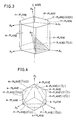
- Fig. 3 is a three dimensional representation of the single crystal of sapphire from which there can be made the substrate 22 of the storage target 20 in accordance with the invention.
- the figure particularly depicts the principal c axis of the sapphire crystal in relation to its c-, - and r-planes.
- the illustrated embodiment takes the r-plane of the sapphire crystal as the storage surface 24 of the substrate 22.
- the reference characters A1, A2 and A3 in Fig. 3 denote the three crystallographic axes of the sapphire crystal, all passing through the C axis and angularly spaced 120 degrees from one another.
- Fig. 4 is a planar representation of the same sapphire crystal, particularly depicting the relationship between its a- and m-planes.
- the c axis of the crystal extends perpendicular to the sheet of this drawing, passing the crossing point of the three crystallographic axes A1, A2 and A3.
- the projection of the c axis of Fig. 3 on a desired crystal plane is meant the projection of the c axis of Fig. 3 on a desired crystal plane.
- the storage surface 24 of the storage target 20 is the r-plane, as has been stated.
- Fig. 5 is drawn to explain, instead, the projection of the c axis on an m-plane.
- Fig. 5 the noted three crystallographic axes A1, A2 and A3 diverge apart from a common point in coplanar relation to one another and at angular spacings of 120 degrees.
- the c axis passes through the common point at right angles with the plane of the crystallographic axes.
- This c axis is projected on the m-plane, shown bounded by the solid lines passing points M1, M2, M3 and M4, as indicated by the dashed lines.
- the projected c axis on the m-plane is designated P'.
- the dashed lines extend right angulary therefrom and fall on the closest points on the m-plane.
- the projections of the c axis on the other planes, r, a, etc., are determined similarly.
- Fig. 6 diagrammatically illustrates an example of scan converter storage tube, generally labelled 32, into which there can be incorporated the storage target 20 of the above improved construc- . tion.
- the storage tube 32 has a hermetically sealed, tubular vacuum envelope 34 housing the storage target 20 adjacent one axial end thereof. Disposed adjacent the other axial end of the vacuum envelope 34 is an electron gun 36 for emitting a modulatable electron beam directed toward the storage target 20.
- the vacuum envelope 34 further accommodates a deflection system 38 and a collimation system 40, which are arranged one after the other along the path of the electron beam from gun 36 to target 20.
- the electron gun 36 comprises a cathode 42, a control grid 44, an acceleration electrode 46, a focusing electrode 48, and an astigmatizer electrode 50.
- the deflection system 38 comprises a pair of vertical deflection plates 52 and a pair of horizontal deflection plates 54 for deflecting the electron beam from the gun 36 vertically and horizontally, respectively.
- the collimation system 40 comprises a wall electrode 56 and a field mesh electrode 58.
- All the components set forth in the preceding paragraph are arranged in that order along the axis of the vacuum envelope 34, in the direction from gun 36 toward target 20.
- the storage target 20 is disposed with the stripes of its collector electrode 26 oriented in the direction of horizontal scanning by the electron beam.
- the cathode 42 of the electron gun 36 may be set at -900 V, and its acceleration electrode 46 at 1 kV with respect to the cathode potential (assumed to be zero).
- the wall electrode 56 of the collimation system 40 may be held at 1 kV, and its field mesh electrode 58 at 2.3 kV, both with respect to the cathode potential.
- the potential of the collector electrode 26 of the storage target 20 with respect to the cathode potential may be 15 V during reading and during writing, may range from one to 10 kV depending upon the frequency band of the input signal.
- the scan converter storage tube 32 of the foregoing construction offers a writing speed of as high as 6500 divisons per microsecond, one division being 1.2 millimeter, as has been ascertained by experiment set forth subsequently.
- the signals to be written may range in frequency from zero (direct current) to several million megahertz. It has been stated in conjunction with Fig. 1 that in the storage target 20 illustrated therein, the stripes 28 of the collector electrode 26 are oriented in the direction of the projected c axis P as indicated by the chordal recess 30 in the storage substrate 22. Experiment has proved that the angle between collector stripes 28 and projected c axis P has a definite relation to the rate at which information can be written on the storage target.
- test storage targets were prepared which were all constructed as in Figs. 1 and 2 except that the angle 0, Fig. 7, between collector stripes 28 and chordal recess 30 (projected c axis P) was varied from one test piece to another.
- the writing speeds afforded by the test storage targets were measured under the same conditions of beam intensity, target voltage, etc.
- Fig. 8 graphically represents the results.
- the writing speed varies in direct proportion with the angle 8, even though all the test targets are of the same materials and of the same configuration except for that angle.
- V1 5000 division/microsecond
- V2 6500 division/ microsecond
- the collector electrode 26 should be oriented in the exact direction of the projected c axis P for the maximum writing speed, as in the storage target 20 of Figs. 1 and 2.
- the angle 6 can be anywhere between minus 45 degrees and plus 45 degrees. For, at plus or minus 45 degrees, the writing speed is approximately 5750 divisions per microsecond, appreciably higher than the above stated value when the angle is plus or minus 90 degrees.
- the collector potential can be made lower than heretofore, affording relative improvement in the voltage withstanding ability of the device.
- the reduction of the collector potential for the write mode is desirable in view of the smaller voltage changes at the time of transitions between the erase (pre-write), write, and read modes.
- the invention proposes the chordal recess 30 in, or any other suitable marking on, each storage substrate 22 to indicate the direction of the projected c axis thereon. Such a marking makes it possible to fabricate collector electrodes in the same direction on respective storage substrates, for the provision of storage tubes offering an invariably high writing speed.
- Fig. 9 shows another preferable form of the storage target in accordance with the invention.
- the modified storage target 120 has a pair of collector electrodes 126 and 126' on the storage surface 24 of the disk-like storage substrate 22.
- the collector electrodes 126 and 126' are each comb- like in shape, having groups of parallel spaced stripes 128 and 128' in staggered arrangement overlying the effective area of the storage surface 24.
- the two staggered groups of stripes 128 and 128' are of course suitably spaced from one another to expose parts of the effective area of the storage surface 24 of the substrate 22.
- the storage surface 24 of the substrate 22 is, preferably, the r-plane of the single sapphire crystal of which the substrate is made.
- the chordal recess 30 is cut in this substrate by way of a marking indicative of the direction of the projected c axis thereon.
- the two staggered groups of collector stripes 128 and 128' both extend in the direction of the projected c axis.
- the two collector electrodes 126 and 126' are electrically disconnected from each other, different voltages are to be applied thereto for writing information in the storage tube incorporating the storage target 120.
- the different voltages produce an electric field between the two collector electrodes for the higher drift velocity of the hole- electron couples generated upon bombardment of the target by the writing electron beam.
- the collector electrodes can then capture the electrons more efficiently and so allow writing at a still higher rate.
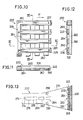
- Figs 10 through 12 show one such storage target 220 embodying the concepts of the invention and intended for use in the direct view storage tube of the type illustrated in Fig. 13.
- This type of storage target, and the direct view storage tube incorporating the same, are both disclosed in the aformentioned Kato et al. U.S. Patent 4,262,230.
- the storage target 220 includes a monocrystalline sapphire storage substrate 222 having a first group of parallel spaced grooves 260 defined in its surface to be directed toward the electron gun of the direct view storage tube.
- a second group of parallel spaced grooves 262 are defined in the opposite surface of the storage substrate 222, to be directed toward the screen, and in right angular relation to the first group of grooves 260.
- the thickness of the first 222 and second 262 groups of grooves are such that they serve to provide in combination an array of openings 264 at their intersections.
- a collector electrode 226 is formed on the gun side surface of the storage substrate 222, and a backing electrode 266 on the screen side surface thereof.
- the collector electrode 226 has a group of electrically interconnected stripes 228 formed on and extending along respective lands 268 between the first group of grooves 260.
- the storage substrate 222 is of course taken along the r-plane of a single sapphire crystal.
- the stripes 228 of the collector electrode 226 extend in the direction of the projected c axis P of the single sapphire crystal on the r-plane.
- the storage target 220 of the above improved construction finds use in the direct view storage tube of Fig. 13.
- the storage tube has a vacuum envelope 270.
- Arranged sequentially within the vacuum envelope 270 are a cathode 272, first grid 274, second grid 276, first anode 278, second anode 280, vertical deflector plates 282, horizontal deflector plates 284, storage target 220, and phosphor screen 286.
- a pair of flood guns 288 are further provided with in the vacuum envelope 270 for use in the read and erase modes.
- the storage target 220 Disposed just behind the screen 286, the storage target 220 has its collector electrode 226 directed toward the electron gun, with the collector stripes 228 oriented horizontally (i.e. the direction in which the beam is deflected by the horizontal deflector plates 284).
- the writing electron beam impinges upon the exposed storage surfaces of the storage substrate 222 in a well known manner.
- the electrons selectively pass through the array of openings 264 in the storage target 220 in accordance with the information stored therein.
- the storage target 220 in the direct view storage tube 232 offers the same advantages as those set forth in connection with the storage target 20 of Figs. 1 and 2.
Landscapes
- Image-Pickup Tubes, Image-Amplification Tubes, And Storage Tubes (AREA)
- Formation Of Various Coating Films On Cathode Ray Tubes And Lamps (AREA)
Applications Claiming Priority (2)
| Application Number | Priority Date | Filing Date | Title |
|---|---|---|---|
| JP212374/82 | 1982-12-03 | ||
| JP57212374A JPS59103248A (ja) | 1982-12-03 | 1982-12-03 | 蓄積タ−ゲツトの製造方法 |
Publications (2)
| Publication Number | Publication Date |
|---|---|
| EP0110283A1 EP0110283A1 (en) | 1984-06-13 |
| EP0110283B1 true EP0110283B1 (en) | 1987-09-16 |
Family
ID=16621502
Family Applications (1)
| Application Number | Title | Priority Date | Filing Date |
|---|---|---|---|
| EP83111622A Expired EP0110283B1 (en) | 1982-12-03 | 1983-11-21 | Storage target for storage tubes and method of fabrication |
Country Status (4)
| Country | Link |
|---|---|
| US (1) | US4532453A (enExample) |
| EP (1) | EP0110283B1 (enExample) |
| JP (1) | JPS59103248A (enExample) |
| DE (1) | DE3373745D1 (enExample) |
Families Citing this family (3)
| Publication number | Priority date | Publication date | Assignee | Title |
|---|---|---|---|---|
| US4599541A (en) * | 1982-12-03 | 1986-07-08 | Iwatsu Electric Co., Ltd. | Scan converter storage tube with a multiple collector storage target, and method of operation |
| FR2595162B1 (fr) * | 1986-02-28 | 1988-05-06 | Labo Electronique Physique | Dispositif d'enregistrement et de restitution de signaux electriques muni d'un predeclenchement, comprenant un dispositif a transfert de charges et oscilloscope utilisant un tel dispositif |
| US5085606A (en) * | 1989-04-12 | 1992-02-04 | Zenith Electronics Corporation | Method of manufacture for post-mask deflection type tension mask color cathode ray tube |
Family Cites Families (7)
| Publication number | Priority date | Publication date | Assignee | Title |
|---|---|---|---|---|
| JPS557946B2 (enExample) * | 1972-04-19 | 1980-02-29 | ||
| JPS5418160U (enExample) * | 1977-04-14 | 1979-02-06 | ||
| JPS5497363A (en) * | 1978-01-19 | 1979-08-01 | Iwatsu Electric Co Ltd | Direct viewing storage tube |
| US4389591A (en) * | 1978-02-08 | 1983-06-21 | Matsushita Electric Industrial Company, Limited | Image storage target and image pick-up and storage tube |
| JPS54140459A (en) * | 1978-04-24 | 1979-10-31 | Hitachi Ltd | Color picture tube and its manufacture |
| JPS5939857B2 (ja) * | 1978-10-09 | 1984-09-26 | 岩崎通信機株式会社 | 走査変換型蓄積管の動作方法 |
| US4407934A (en) * | 1981-12-04 | 1983-10-04 | Burroughs Corporation | Method of making an assembly of electrodes |
-
1982
- 1982-12-03 JP JP57212374A patent/JPS59103248A/ja active Granted
-
1983
- 1983-11-18 US US06/553,483 patent/US4532453A/en not_active Expired - Fee Related
- 1983-11-21 EP EP83111622A patent/EP0110283B1/en not_active Expired
- 1983-11-21 DE DE8383111622T patent/DE3373745D1/de not_active Expired
Also Published As
| Publication number | Publication date |
|---|---|
| EP0110283A1 (en) | 1984-06-13 |
| JPS59103248A (ja) | 1984-06-14 |
| JPH022254B2 (enExample) | 1990-01-17 |
| DE3373745D1 (en) | 1987-10-22 |
| US4532453A (en) | 1985-07-30 |
Similar Documents
| Publication | Publication Date | Title |
|---|---|---|
| US2547638A (en) | Image storage tube | |
| US3531675A (en) | Cathode ray storage tube having a target dielectric with collector electrodes extending therethrough | |
| EP0110283B1 (en) | Storage target for storage tubes and method of fabrication | |
| US3683224A (en) | Low depth cathode ray tubes | |
| US3148304A (en) | Single-beam color picture tube employing venetian blind deflection grid | |
| CA1105542A (en) | Box-shaped scan expansion lens for cathode ray tube | |
| US3956662A (en) | Cathode ray storage tube having a target dielectric provided with particulate segments of collector electrode extending therethrough | |
| GB1534795A (en) | Device for localizing light phenomena | |
| US2806174A (en) | Storage tube | |
| US3356878A (en) | Signal converting cathode ray tube with controllable erasure | |
| US4215288A (en) | Storage target for scan converter tubes | |
| Newman et al. | Dot matrix electron beam lithography | |
| JPS61264640A (ja) | 画像表示装置 | |
| US5061875A (en) | Focus electrode for elongated hexagonal photomultiplier tube | |
| EP0111201B1 (en) | Scan converter storage tube with a multiple collector storage target, and method of operation | |
| US3541384A (en) | Image storage apparatus | |
| US3940651A (en) | Target structure for electronic storage tubes of the coplanar grid type having a grid structure of at least one pedestal mounted layer | |
| US3675134A (en) | Method of operating an information storage tube | |
| EP0461657A2 (en) | Flat display | |
| US4288720A (en) | Method of erasing information in a scan converter storage tube | |
| SU892522A1 (ru) | Плоский вакуумный индикатор | |
| US2713650A (en) | Electron discharge devices | |
| US3997812A (en) | Digitizing matrix for electron beams | |
| Lee | Electron Gun for LEED Applications | |
| US4282456A (en) | Faceplate for an electrostatic printing tube and method of making same |
Legal Events
| Date | Code | Title | Description |
|---|---|---|---|
| PUAI | Public reference made under article 153(3) epc to a published international application that has entered the european phase |
Free format text: ORIGINAL CODE: 0009012 |
|
| AK | Designated contracting states |
Designated state(s): DE FR NL |
|
| 17P | Request for examination filed |
Effective date: 19840913 |
|
| 17Q | First examination report despatched |
Effective date: 19860314 |
|
| GRAA | (expected) grant |
Free format text: ORIGINAL CODE: 0009210 |
|
| AK | Designated contracting states |
Kind code of ref document: B1 Designated state(s): DE FR NL |
|
| REF | Corresponds to: |
Ref document number: 3373745 Country of ref document: DE Date of ref document: 19871022 |
|
| ET | Fr: translation filed | ||
| PLBE | No opposition filed within time limit |
Free format text: ORIGINAL CODE: 0009261 |
|
| STAA | Information on the status of an ep patent application or granted ep patent |
Free format text: STATUS: NO OPPOSITION FILED WITHIN TIME LIMIT |
|
| 26N | No opposition filed | ||
| PGFP | Annual fee paid to national office [announced via postgrant information from national office to epo] |
Ref country code: FR Payment date: 19911018 Year of fee payment: 9 |
|
| PGFP | Annual fee paid to national office [announced via postgrant information from national office to epo] |
Ref country code: NL Payment date: 19911130 Year of fee payment: 9 |
|
| PGFP | Annual fee paid to national office [announced via postgrant information from national office to epo] |
Ref country code: DE Payment date: 19920131 Year of fee payment: 9 |
|
| PG25 | Lapsed in a contracting state [announced via postgrant information from national office to epo] |
Ref country code: NL Effective date: 19930601 |
|
| NLV4 | Nl: lapsed or anulled due to non-payment of the annual fee | ||
| PG25 | Lapsed in a contracting state [announced via postgrant information from national office to epo] |
Ref country code: FR Effective date: 19930730 |
|
| PG25 | Lapsed in a contracting state [announced via postgrant information from national office to epo] |
Ref country code: DE Effective date: 19930803 |
|
| REG | Reference to a national code |
Ref country code: FR Ref legal event code: ST |