EP0109880B1 - Dispositif de traitement de la parole pour équipement émetteur-récepteur radioélectrique adapté pour la transmission et la réception de la parole - Google Patents
Dispositif de traitement de la parole pour équipement émetteur-récepteur radioélectrique adapté pour la transmission et la réception de la parole Download PDFInfo
- Publication number
- EP0109880B1 EP0109880B1 EP19830402124 EP83402124A EP0109880B1 EP 0109880 B1 EP0109880 B1 EP 0109880B1 EP 19830402124 EP19830402124 EP 19830402124 EP 83402124 A EP83402124 A EP 83402124A EP 0109880 B1 EP0109880 B1 EP 0109880B1
- Authority
- EP
- European Patent Office
- Prior art keywords
- speech
- circuit
- signal
- phase
- received
- Prior art date
- Legal status (The legal status is an assumption and is not a legal conclusion. Google has not performed a legal analysis and makes no representation as to the accuracy of the status listed.)
- Expired
Links
- 230000005540 biological transmission Effects 0.000 title claims description 54
- 238000012937 correction Methods 0.000 claims description 33
- 230000006835 compression Effects 0.000 claims description 24
- 238000007906 compression Methods 0.000 claims description 24
- 230000006870 function Effects 0.000 claims description 11
- 238000012545 processing Methods 0.000 claims description 10
- 230000007423 decrease Effects 0.000 claims description 7
- 238000000034 method Methods 0.000 claims description 6
- 230000008859 change Effects 0.000 claims description 5
- 230000001755 vocal effect Effects 0.000 claims description 4
- 230000003111 delayed effect Effects 0.000 claims description 3
- 230000002238 attenuated effect Effects 0.000 claims description 2
- 230000008569 process Effects 0.000 claims description 2
- 230000001174 ascending effect Effects 0.000 claims 9
- 238000012163 sequencing technique Methods 0.000 description 15
- 238000001914 filtration Methods 0.000 description 14
- 230000006978 adaptation Effects 0.000 description 8
- 230000009471 action Effects 0.000 description 5
- 238000001228 spectrum Methods 0.000 description 5
- 238000010586 diagram Methods 0.000 description 4
- 230000012010 growth Effects 0.000 description 4
- 230000007704 transition Effects 0.000 description 4
- 230000008054 signal transmission Effects 0.000 description 3
- 230000003044 adaptive effect Effects 0.000 description 2
- 230000003698 anagen phase Effects 0.000 description 2
- 238000013475 authorization Methods 0.000 description 2
- 230000000694 effects Effects 0.000 description 2
- 238000005562 fading Methods 0.000 description 2
- 238000002360 preparation method Methods 0.000 description 2
- 230000035945 sensitivity Effects 0.000 description 2
- 238000003860 storage Methods 0.000 description 2
- 238000012790 confirmation Methods 0.000 description 1
- 230000003247 decreasing effect Effects 0.000 description 1
- 230000006735 deficit Effects 0.000 description 1
- 230000006872 improvement Effects 0.000 description 1
- 238000004519 manufacturing process Methods 0.000 description 1
- 238000000819 phase cycle Methods 0.000 description 1
- 238000003672 processing method Methods 0.000 description 1
- 238000012797 qualification Methods 0.000 description 1
- 238000011084 recovery Methods 0.000 description 1
- 230000009467 reduction Effects 0.000 description 1
- 230000003068 static effect Effects 0.000 description 1
- 230000001360 synchronised effect Effects 0.000 description 1
- 230000002123 temporal effect Effects 0.000 description 1
Images
Classifications
-
- H—ELECTRICITY
- H04—ELECTRIC COMMUNICATION TECHNIQUE
- H04B—TRANSMISSION
- H04B1/00—Details of transmission systems, not covered by a single one of groups H04B3/00 - H04B13/00; Details of transmission systems not characterised by the medium used for transmission
- H04B1/62—Details of transmission systems, not covered by a single one of groups H04B3/00 - H04B13/00; Details of transmission systems not characterised by the medium used for transmission for providing a predistortion of the signal in the transmitter and corresponding correction in the receiver, e.g. for improving the signal/noise ratio
- H04B1/64—Volume compression or expansion arrangements
Definitions
- the present invention relates to a speech processing device for radio transmitter-receiver equipment suitable for transmitting and receiving speech, which can be used, in particular, in radiotelephony.
- Analog speech processing systems for radio transmission of the type known under the name "LINCOMPEX” are known, a description of which can be found in US Pat. No. 4,271,499, which allow using variable attenuation on transmission maintain an almost constant level of speech modulation for a period close to a few tens of milliseconds, which notably improves the signal / noise ratio obtained on reception.
- the value of the attenuation introduced on transmission is transmitted by an auxiliary frequency multiplexed channel, by frequency modulation of a subcarrier located at the top of the telephone band, to control an expander located at the level of the receiver, which is none other than an attenuator operating opposite to that of the transmitter, so as to recover the level of speech existing before its compression.
- purely analog systems are used in radiotelephony in the HF range.
- SYNCOMPEX An improvement to the “LINCOMPEX” system is known under the name “SYNCOMPEX”.
- speech is processed in packets of finite duration (13.33 milliseconds) and an auxiliary channel in the form of an auxiliary frequency radio channel is coded in digital.
- the corresponding codes are transmitted by a frequency hopping modulation system of the "FSK” type where "FSK” is the abbreviation of the English term “Frequency shift keying”, and working in diversity on two subcarriers introduced in the band vocal.
- FSK frequency hopping modulation system
- Frequency shift keying the speech components existing in the bands used to transmit the “FSK” channels are eliminated.
- Diversity transmission makes it possible, by transmitting digital information according to two different channels, to choose at reception the channel which has the best signal / noise ratio and therefore to minimize transmission errors.
- the syllabic term has a large amplitude of around 30 decibels for a speaker and its frequency band ranges from very low frequencies to ten hertz, the average syllabic cadence being generally close to 4 to 7 hertz.
- the syllabic term is in practice not significant for speech intelligibility and has little effect on pleasure. It is however used in transmission, to improve listening comfort, by suppressing radio noise in speech silences and in traditional telephony, by keeping the equivalent, to stabilize the amplifier circuits.
- the melodic term has a more limited amplitude of 10 to 15 decibels and its frequency band covers a spectrum of 60 to 250 hertz according to the individuals.
- the melodic term is on the other hand extremely significant for the pleasure of the hearing and the recognition of the speaker, the reproduction of its frequency is therefore particularly important.
- the transmission noise contains at least as many harmonic frequencies of the melodic spectrum as significant syllabic adaptation signals, which causes reception errors which cannot be eliminated by methods. simple processing using, for example, analog filters.
- the object of the present invention is to remedy the aforementioned drawbacks.
- the subject of the invention is a device for processing speech of radio transmitter and receiver equipment suitable for transmitting and receiving speech, of the type comprising a circuit for compressing the dynamics of the speech signal. to maintain the level of speech modulation roughly constant during the transmission of speech and an expander to restore upon reception the level of speech before its compression, as well as a device for controlling the expander sensitive to value of the attenuation introduced by the compression circuit, and transmitted over an auxiliary frequency radio channel of the equipment, characterized in that the compression circuit is an incremental compression circuit, with early action in time comprising a line delay connected to a first variable attenuator to delay the speech signal and attenuate it before its emission as well as a second variable attenuator of the speech signal, and in that the device further comprises a logic filtering circuit of the transmission speech level coupled to the second variable attenuator for controlling the first and second attenuators of the compression circuit by constant attenuation steps so as to maintain the speech level d almost constant emission and to transmit by the auxiliary channel the incremental attenu
- the advantages obtained by the device according to the invention are, on the one hand, to make it possible to constitute a true filtering device on reception, to separate the noise from the significant adaptation signals and, on the other hand, as a corollary, correct the transmission errors which would generate a spurious signal whose frequency spectrum would contain frequencies of the melodic spectrum.
- the first objective is achieved, thanks to the incremental compressor with early action in time which allows the anticipation of the adaptation signal by delaying the speech signal, so as to correctly transmit the beginnings of the syllables where the amplitude increases rapidly, those -this being transmitted in phase with the adaptation signals.
- the transmission of the adaptation signals makes it possible to obtain on reception a better quality of the decisions which must be taken at the level of the preparation of the orders.
- adaptation while allowing by suitable means to bring the adaptation signal back into temporal coincidence with the received acoustic signal.
- the second objective is achieved by the interpolation circuit which makes it possible to correct the transmission errors liable to produce an adaptation signal whose frequencies correspond to those of the melodic spectrum.
- the combined actions of the logic filter and the delay introduced into the transmission of the speech signal by the early action compression circuit allow a significant reduction in the bandwidth of the auxiliary channel.
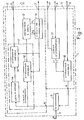
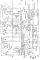
- the device 1 comprises a transmission part 2 and a reception part 3. It is connected to a telephone line 4 on which the speech signals pass through via a hybrid transformer 5
- the input of the hybrid transformer 5 which is not connected to the telephone line 4 is directly connected to the output R of the reception part 3 and the output of the transformer 5 is directly connected to the input E of the transmission part 2
- the transmission part 2 of the device is connected by an output 6 to the radio transmission circuit of the transmitter, not shown, and transmits a speech signal to the latter, the level of which is kept approximately constant.
- the transmission part 2 also includes an output 7 which is connected to the transmission circuit of the transmitter, not shown, for transmitting the coded level information on an auxiliary channel of the transmitter not shown.
- the reception part 3 comprises an input 8 which is connected to the reception circuit, not shown, of the transceiver, to receive the demodulated speech signal.
- the reception part also includes an input 9 and an input 10.
- the input 9 is connected to the reception circuit of the transceiver, not shown, connected to the auxiliary level channel.
- the input 10 is connected to the demodulation circuit (not shown) of the receiver and receives from the latter a weighting signal e, when an uncertainty exists on the demodulated content of the information received by the auxiliary channel.
- the transmission part 2 consists of a compression circuit 11 connected to a threshold detector 12 and a filtering circuit 13.
- the compression circuit 11 consists of a delay line 14, located between the input E of the transmission part and the input of a variable attenuator 15.
- the compression circuit 11 also includes a variable attenuator 16 whose input is connected to the input E of the emission part 2 and whose output is connected to the input of the detector at threshold 12.
- the threshold detector 12 is connected by its outputs Si and S 2 to respective inputs of the logic filtering circuit 13.
- the logic filtering circuit 13 comprises two outputs, one of which is connected to output 7 of the device and the other of which is connected to the control inputs of the variable attenuators 15 and 16.
- the output of the variable attenuator 15 is connected to the output 6 of the device for transmitting the transmission speech signal.
- the reception part consists of an interpolation circuit 17 connected by two inputs to the inputs 9 and 10 of the device 1 which respectively receive the level information received by the auxiliary channel and the weighting signal e, the presence of which is characteristic of a presumption of error on the simultaneous level information received.
- the interpolation circuit 17 has an output directly connected to the control input of the variable attenuator 18.
- the variable attenuator 18 has an input directly connected to the terminal 8 of the device 1 to receive the speech signal demodulated by the receiver circuits, not shown, and an output directly connected to output R of the reception part.
- the operation of the device shown in Figure 1 is as follows.
- the speech signal which is transmitted by the telephone channel 4 is applied to the input E of the reception part 2 via the hybrid transformer 5.
- the speech signal crosses the compression circuit 11 successively through the line delay 14 and the attenuator 15 and exits on the output 6 of the device 1.
- the threshold detector 12 indicates the changes in power level of the non-delayed speech signal, passing through the attenuator 16 to the circuit logic filtering 13 via outputs Si and S 2 .
- the logic filtering circuit 13 as a function of the level changes detected by the threshold detector 12, controls the attenuators 15 and 16 and the coding of the level information which is transmitted by the terminal 7.
- the speech signal On reception, the speech signal, demodulated by the receiver circuits, not shown, is applied to terminal 8 at the input of the variable attenuator 18 which is controlled by the interpolation circuit 17.
- the variable attenuator 18 controlled by the interpolation circuit 17 ensures the dynamic expansion of the speech signal, to reconstruct, at the input of the hybrid transformer 5, the speech signal with its original dynamic restored.
- the interpolation circuit 17 uses the coded level information, containing the level attenuation decisions transmitted by the auxiliary level channel applied to the input 9 as well as the weighting signal e, applied to the input 10 which will for example be a simple signal to erase the decision to modify the level attenuation received.
- This solution will be applicable, in particular whenever the radio transmission is affected by fading and the level information transmitted on the level channel is interleaved in a digital frame containing the speech channel.
- a speech transmission at 16 k / bits per second it will thus be possible to transmit corresponding binary information on the level channel every 48 bits. It will therefore be possible, in this case, to provide a qualification signal valid for the 49 bits in the event of fading.
- the control decision of the attenuator 18 will be taken taking into account the constraints imposed for the transmission of the signal to restore to the erased binary elements, values introducing the minimum of components located in the melodic frequency band.
- the attenuators 15, 16 and 18 used for carrying out the preferred mode of the invention are static incremental attenuators, constituted in the manner of a weight box, which can be introduced step by step at a determined clock rate differential attenuation, for example, 0, +3, -3 decibels every 6 milliseconds.
- the coding of the level information may consist of a series of binary elements having a first configuration when the level before compression of the syllabic term of the speech is in positive growth phase, a second configuration when the level of the syllabic term of the speech is in negative decay phase and at least a third configuration when the level of the syllabic term retains an almost constant value.
- coding of the “delta” type is used to code the level information.
- the increment commands provided by the filter logic and by the interpolation circuit will only be made effective when 2 level coding signals, received consecutively, have the same value.
- a and Z respectively designate the signals of the “delta” coding used, an increase or a decrease in the speech level above or below the acceptable thresholds will be coded using 2 consecutive ZZ signals to control an attenuation of +3 decibels and using 2 consecutive AA signals to control an attenuation of -3 decibels. No attenuation will be commanded when the consecutive received signals are alternated, combined in the ZA or AZ manner.
- the transmission of signals A and Z on the auxiliary channel is carried out using a subcarrier of frequency f o for the transmission of signal A and a subcarrier of frequency f 1 for the transmission of signal Z.
- the device may not take any decision to increment when one of the two signals A or Z will be marked by the simultaneous presence of the weighting signal e indicating a presumption of error on the received signal.
- control of the attenuators may take place so as to take into account only the level variations corresponding to the syllabic term of the speech, while respecting the consecutive alternating phases of growth and decay.
- the duration of the commands will be chosen so that the fundamental frequency of the attenuator control signals does not exceed 10 hertz.
- the increase command will be carried out when the peak signal detected by the detector 12 exceeds a first threshold and the decay command will be carried out when the signal detected by the threshold detector 12 during an elementary period of time is lower at a second threshold, for example, less than a threshold of 3 decibels at the first threshold for a duration greater than the longest melodic period, that is to say approximately 18 milliseconds, with the first threshold not being exceeded during this time.
- a second threshold for example, less than a threshold of 3 decibels at the first threshold for a duration greater than the longest melodic period, that is to say approximately 18 milliseconds, with the first threshold not being exceeded during this time.
- variable attenuators 15 and 16 are within the competence of a person skilled in the art, they could be produced for example, by bridges of attenuation resistors, connected electronically by means of PIN diodes.
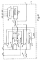
- the filtering logic 13 is constituted by a clock 19, an up-down counter 20, a rocker 21 controlled by doors 22 and 23 , a counter 24 associated with an AND gate 24 bis, OR gates 25 and 26, a timer counter 27, a decoder 28 connected by its inputs to the outputs of the up-down counter 20 as well as an encoder 29 of the level information .
- the up-down counter 20 delivers on its outputs signals which are decoded by the decoder 28 to control the attenuation value of the attenuators variables 15 and 16.
- the up-down counter 20 is controlled through the encoder 29 in counting mode, on its input marked “+”, by the output of gate AND 22 and in down-counting mode, on its input marked “- »By the exit of door ET 24 bis.
- the AND gate 22 has three inputs, a first input is connected to the output Si of the threshold detector 12 which transmits the signal for exceeding the speech level above the first threshold, a second input is connected to the output of the clock 19 and the third input is connected to the output of the OR gate 25.
- the OR gate 25 has two inputs, a first input is connected to the output Q of the rocker 21 and the second input is connected to the first input of the gate OR 26 as well as at the output marked T of the counter 27.
- the AND gate 23 has two inputs, a first input is connected to the output of the clock 19 and the second input is connected to the output of the OR gate 26.
- the output of the AND gate 23 is connected, on the one hand, to a first input of the AND gate 24 bis and on the other hand, to the counting input of the counter 24.
- the counting output of the counter 24 is connected at the second entrance of gate ET 24 bis.
- the counter reset input 24 is connected to the output S 2 of the threshold detector of FIG. 1. In this way the counter 24, controlled by the clock 19 with authorization from the OR gate 26 by the AND gate 23, is reset to zero by the presence of a signal on the output S 2 of the threshold detector 12. If the signal at the output S 2 of the threshold detector 12 is absent for a determined number of clock pulses 19 , the counter 24 adds up the corresponding number of pulses and at the end of the counting commands the opening of the gate 24 bis.
- the OR gate 26 has two inputs, a first input is connected to the output marked T of the counter 27 and the second input is connected to the output Q of the rocker 21.
- the clock input of the counter 27 is connected to the output of the clock 19 and has its reset reset input connected to the rocker 21 which transmits a reset pulse to the counter 27, each time the rocker 21 changes state.
- the outputs of the decoder 28 are connected directly to the control inputs of the variable attenuators 15 and 16, to transmit the attenuation values at constant pitch of 3, 6, 12 decibels etc ... and modify their attenuation rate in successive steps +3 or -3 decibels.
- the encoder 29 has its inputs connected respectively to the outputs of the AND gates 22 and AND 24 bis and transmits to the transmission circuits not shown, in synchronism with the clock signals delivered by the clock 19, signals for coding the information of level, by the “delta” type coding previously described, as well as the up and down counting signals applied to the “+” and “-” inputs of the up-down counter 20.
- the operation of the filter logic 13 shown in Figure 2 is as follows.
- the clock signal supplied by the clock 19 is a binary signal with two states of period 6 milliseconds and is applied respectively to the corresponding inputs of the AND gates 22, 23.
- the clock signal is retransmitted by the AND gate 22, when an overshoot signal is delivered by the output Si of the threshold detector 12 of FIG. 1 and when the AND gate 22 is validated by the output of the OR gate 25.
- the clock signal delivered by the clock 19 is applied to the corresponding input of AND gate 23 and is retransmitted by the output of AND gate 23 when authorization is given by the output of OR gate 26.
- the output signal of AND gate 23 makes advance the counter 24. If a signal for exceeding the second threshold appears on the output S 2 of the threshold detector 12 of FIG.
- the counter 24 is reset to zero.
- the counter 24 has counted 3 pulses of 6 ms, ie 18 ms, its output commands the opening of the AND gate 24 bis.
- the output pulses of the AND gates 22 and 24 bis respectively control the inputs marked "+" and "-" of the rocker 21 and the encoder 29.
- the encoder 29 emits, at each clock pulse 19, a binary signal whose value is a function both of the value of the previous binary signal and of the variation control which is in the positive, negative or zero hypothesis. In the case of a zero variation, that is to say of absence of variation of the voice level, the binary signal emitted by the encoder 29 will be the inverse of the previous signal.
- the up-down counter 20 is controlled by the output of the encoder 29 on its "+” input each time the voice signal increases and on its "-” input each time the voice signal decreases.
- the counter 27 is reset to zero, then it advances step by step at each clock pulse spaced 6 milliseconds apart.
- the output T of the up-down counter 27 authorizes through the OR gates 25 and 26 the passage of the pulses incremental control commands, supplied by the clock 19, through doors 22 and 23.
- doors 22 and 24 bis are validated respectively by one of the outputs Si or S 2 of the threshold detector 12, in progress for counting the counter 27, the AND gate 22 is only authorized if the rocker 21 already has its output Q at state 1 and the gate 24a is only authorized, through the AND gate 23, only if the rocker 21 has its output Q at state 1, which prohibits, by this embodiment, the counting and counting down changes and vice versa, if a determined time of 42 milliseconds has not elapsed since the first signal of the same phase or the last phase change.
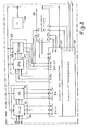
- the interpolation circuit 17 comprises, a set of shift registers 30, composed of the subsets of registers 31 and 32, a second set of shift registers 33 composed of the subsets 34 and 35, a circuit 37 for correcting the signals representing the level information received, a circuit incrementation 38 to control more or less an attenuation level of the attenuator 18, as well as a phase sequencer 39.
- a clock 36 ensures synchronization between all the elements of the interpolation circuit 17.
- the sub -set of shift register 31 has its inputs connected directly to input 9 of device 1 of FIG.
- the subset of registers 31 is also connected to the input 10 of the device 1 of FIG. 1 to receive the binary erasure decision and reversing when present the decision corresponding to the signal A or Z present on the input 9
- the use of the erase signal e constitutes a simple method of weighting, which is particularly advantageous, when the transmission is subjected to significant variations in the signal / noise ratio or if the transmission is strongly interfered with.
- the signals e, A, Z applied to the input of the shift sub-assembly 31 are stored in the latter, as soon as the pulse of the clock signal transmitted by the clock 36 appears and are transferred to the instant of appearance of the next clock pulse, of the subset of the register 31 in the subset of the register 32.
- the subset 32 therefore contains at each instant n + 1 the appearance of a pulse d clock, the data D n representing the decisions e, A, Z received at the instant n of publication of the preceding clock pulse and the subset 31 records, at each instant of publication of a pulse of clock, the data D n + i representing the decisions e, A, Z which are currently received by the reception device.
- the data D n and D n + i are transmitted to the corresponding inputs of the correction circuit 37 which aims to correct the decisions A or Z retransmitted by the demodulation circuit, not shown, to the interpolation circuit 17, taking into account constraints introduced on the transmission signals and which correspond to the conditions of succession of three binary elements, imposed by the device to authorize the control of the attenuators, in relation to the decisions A c or Z c earlier already corrected or those I judged by the device as indeterminate.
- the correction circuit 37 prepares the corrections as a function of the corrected decisions D (n-1) c of the instant n-1, and of the phase information P + and P- reconstructed by the phase sequencer 39.
- the subset of register 34 is connected by its inputs to the correction circuit 37 to store the corrected decisions A c Z r produced by the correction circuit 37.
- the data stored inside the registers 34 are transferred, at the instant of the pulse next clock, in the subset of registers 35 which thus stores the corrected data D (n-1, c of the instant n-1 and which will be used to correct the decisions of the instant n.
- the sub- set of registers 35 is for this purpose connected by its outputs to corresponding inputs of the correction circuit 37, to allow the correction circuit 37 the preparation of correction data from the current data received at time n, as a function of the data already corrected from time n-1.
- the correction data established by the correction circuits 37 are also transmitted to the incrementation circuit 38 to calculate at each instant n the increment rate +1 or -1 which must be applied by the interpolation circuit 17 on the control input of the variable attenuator 18 of FIG. 1.
- the correction circuit 37 also supplies the signals PP + and PP- of presumption of transition to the positive phase of incrementation and of presumption of transition to the negative phase of decrementation as well as the correction decisions A c and Z c intended for the corresponding inputs of the phase sequencer 39 in order to verify that on reception the constraints imposed by the logic filtering circuit 13 on transmission (FIG. 1) are well respected.
- phase sequencer 39 which reconstructs the positive or negative phases of growth and decay of the speech signal determined on transmission, applies the phase conditions P + and P- reconstructed to the corresponding inputs of the correction circuit 37.
- the conditions phase P + and P- are also established as a function of signals +1 and -1 transmitted by the incrementation circuit 38 to the corresponding inputs of the phase sequencer 39 which correspond to the decisions of increments +1 and -1.
- the correction circuit 37 is formed by all of the doors. 40 to 46.
- Door 40 determines with door 41 the decision to correct A c of the information received.
- Gate 40 is an OR gate with two inputs, connected respectively to the output of gate 41 and to the corresponding output of registers 32 which transmits the decision signal A. The output of gate 40 transmits the corrected decision A c when either , a decision A is transmitted by the register 32 or when a PP + positive phase presumption signal is transmitted by the output of gate 41.
- the PP + signal is transmitted by gate 41 at each time n + 1 when erase signal "e" is supplied by the reception demodulator at the instant n preceding while the phase sequencer 39 of FIG. 3 indicates that the device processes a voice signal in phase P- of decay and that the signals of decision received at times n-1 and n + 1 are Z signals.
- gate 41 is an AND gate with three inputs, a first input is connected to the output of an OR gate 42 with two inputs. A second input is connected to the phase sequencer 39 and receives the phase indication signal P; the third entry is connected to the register subset 32 and receives the erasure decision "e".
- a first input of the OR gate 42 is connected to the storage subset 35 and receives the decision Z c corrected by the instant n-1. The second input of OR gate 42 is connected to the subset of storage 31 and receives the decision Z from time N +1.
- gate 43 determines with the gate 44 the decision to correct Z e of the information received.
- Gate 43 is an OR gate with two inputs connected respectively to the output of gate 44 and to the corresponding output of registers 32 which transmits the decision signal. The output of gate 43 transmits the corrected decision Z c when either, a decision Z is transmitted by the registers 32 or when a signal PP- of negative phase presumption is transmitted by the output of gate 44.
- the signal PP- is transmitted by gate 44 at each instant n +1 when an erasure signal "e" has been transmitted by the reception demodulator at the preceding instant n while the phase sequencer indicates that the device is processing a voice signal in the “+” phase of growth and that the decisions obtained at reception at times n-1 and n + 1 are decisions A.
- the gate 44 is an AND gate with three inputs, a first input is connected to the corresponding output of the phase sequencer 39 which transmits the P + growth phase information, the second input is connected to the output of the OR gate 45 which receives on a first input the corrected decision A c contained in the subset of register 35 and on its second entry the decision A contained in the register subset 31.
- the third input of gate 44 is connected to the corresponding output of registers 32 which transmits the erasure signal.
- the corrections provided by gates 40 and 43 therefore express the fact that in the negative phase there cannot be a consecutive sequence of decisions Z, (ZZ), and that in the positive phase there cannot be a consecutive sequence of decisions A, (AA).
- the outputs of doors 40 and 43 are connected to the respective inputs of the NAND AND gate 46.
- the output of door 46 delivers a decision I, indeterminate, if no decision A e or Z c appears at the outputs of doors 40 and 43.
- the incrementing circuit 38 is formed by logic circuits 47 to 59.
- the incrementing command marked "+1" is provided by the output of the OR gate 47 with two inputs, a first input of which is connected to the output of the gate AND 48.
- the AND gate 48 has two inputs, a first input is connected to the output of the OR gate 43 and the second input receives the signal Z c stored inside the subset of registers 35.
- circuits 47 and 48 authorize an increment of +3 decibels of the reception attenuator when the decisions contained in registers 32 and 35 both correspond to a decision Z e .
- the -3 decibel decrement command is provided by the output of the OR gate 49 with two inputs, a first input of which is connected directly to the AND gate 50 with two inputs.
- a first input of the AND gate 50 is connected directly to the output of the OR gate 40 and the second input of the AND gate 50 directly receives the corrected decision A e contained in the subset of registers 35.
- a decrementation command of -3 decibels is therefore provided by the OR gate 49 and by the AND gate 50, if the decisions contained in the subsets of registers 32 and 35 both correspond to a corrected decision A c .
- the attenuation of the variable attenuator 18 in FIG. 1 remains unchanged.
- circuits 51 to 59 makes it possible to treat the cases which, taking into account the phase in which the device is located, can be counted on average, either for an incrementation of 1/2 in positive phase, or for an increment of -1/2 in negative phase. These cases are collated on the inputs of doors 51 and 52 with three inputs.
- the AND gate 51 is connected by a first input to the output of an OR gate 53 with two inputs, a first input of which is connected directly to the output of the AND gate 54.
- the AND gate 54 has two inputs, a first input receives the corrected decision A c contained in the subset of registers 35 and the second input is connected directly to the output of the NAND gate 46.
- the second input of the OR gate 53 receives the indeterminate decision i of the subset of registers 35.
- the second input of AND gate 51 receives the phase signal P- from the phase sequencer 39.
- the third input of AND gate 51 is connected directly to the output of inverter 55.
- the output of gate 51 is directly connected to the input of the bistable rocker 56, the output of which is connected directly to the second input of the OR gate 49.
- the rocker 56 is controlled by the AND gate 51 each time that, on the one hand, the device is in negative phase P- that, on the other hand, the decision taken at an instant n + 1 contained in the register 31 is not an erasure, and that the decision taken at the previous instant n was undetermined while the decision taken at instant n-1 was a decision A.
- the AND gate 52 has a first input connected to the output of an OR gate 57 with two inputs.
- a first input of the OR gate 57 is connected to the output of the AND gate 58 with two inputs, a first input of which is connected to the output of the NAND circuit 46 and the second input of which receives the corrected decision contained in the sub- set of registers 35.
- the second input of the AND gate 52 receives the phase signal P + transmitted by the phase sequencer 39 of FIG. 3.
- the third input of the AND gate 52 is connected directly to the output of the inverter 55
- the output of the AND gate 52 is connected directly to the input of a bistable rocker 59 the output of which is connected directly to the second input of the OR gate 47.
- the rocker 59 is controlled by the AND gate 52 each time that, on the one hand, the device is in positive phase P +, that, on the other hand, the decision taken at an instant n + 1 contained in the register 31 n ' is not an erasure and that the decision taken at time n was undetermined, whereas the decision taken at time n-1 was a decision Z.
- All circuits 49 and 59 allow recovery of indeterminate decisions which negative phase can be considered as having an average value of 1/2, since they cannot be corrected either in 0 or in +1.
- the rockers 56 and 59 eliminate one decision out of two, transmitted by the gates 51 and 52 and the increments which they memorize are added to those transmitted respectively by the gates 48 and 50 by means of the circuits OR 47 and 49.
- the increments + 1 and -1 transmitted respectively by gate 47 and 49 are applied to the attenuator at each clock pulse.
- the signals 1+ and I- which correspond to the direct decisions of incrementation and decrementation are transmitted by the gates 48 and 50 to the phase sequencer.
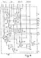
- the phase sequencer represented in FIG. 5 comprises, a positive phase sequencing device 60, a sequencing device of “intermediate” phase 61 and a negative phase sequencing device 62.
- the positive phase sequencing device comprises, a counter 63 connected on its counting input to a rocker 64 through an AND gate 65 with two inputs.
- the first input of the AND gate 65 is connected to the clock 36 of FIG. 3.
- the second input of the AND gate 65 is connected to the output of the rocker 64.
- a first input of the rocker 64 is connected to the output of an AND gate 66 with two inputs, and the second reset input of the rocker 64 is connected to the output of an OR gate 68 with two inputs.
- the “intermediate” phase sequencing device 61 also includes a counter 69 connected on its counting input to the output of a rocker 70 through a door 71 with two inputs.
- a first input of the door 71 is connected to the output of the clock 36 of FIG. 3 and the second input of the door 71 is connected to the output of the rocker 70.
- the rocker 70 is connected on its first input to the output of an AND gate with two inputs 72 and by its second reset input at the output of an OR gate 73 with two inputs.
- the negative phase sequencing device 62 also includes a counter 74 connected on its counting input to the output of an AND gate 76 with two inputs.
- a first input of the AND gate 76 is connected to the output of the clock 36 of FIG. 3 and the second input is connected to the output of the rocker 75.
- the control input of the rocker 75 is connected to the output of an AND gate 77 with two inputs and the reset input of the rocker 75 is connected to the output of an OR gate 79 with two inputs.
- the phase sequencing devices 60, 61, 62 are synchronized from the circuit 80 composed of the logic elements 81 to 89 as well as by the circuits 90 to 98.
- the circuit 80 comprises four AND gates with two inputs 81 to 84.
- the outputs of the doors 81 and 82 are respectively connected to the corresponding inputs of an OR gate 86 whose output is connected to the control input of a rocker 87.
- the outputs of doors 83 and 84 are respectively connected to the corresponding inputs of an OR gate with two inputs 85, the output of which is connected to the control input of a rocker 88.
- the outputs of the rockers 87 and 88 are respectively connected to the corresponding inputs of an AND gate 89 with two inputs.
- the gates 81 and 82 receive on a first input the corrected decision Z r coming from the correction circuit 37 of FIG. 3 and the gates 83 and 84 receive on a first input the corrected decision A c coming from the correction circuit 37 of FIG. 3.
- the second inputs of doors 81 to 84 are respectively connected to outputs of the counter 69.
- the output of door 89 is connected to a first input of an OR gate 90 with two inputs, the second input of which receives the I + signal from of the incrementation circuit 38 of FIG. 3.
- the output of the OR gate 90 is connected to the reset inputs of the counter 69 and of the rockers 87 and 88.
- the logic circuit 91 is a rocker whose state indicates at l 'the whole device to which positive or negative phase, denoted P + or P-, correspond to the signals received.
- the rocker 91 is controlled by the outputs of doors 92 and 93.
- the AND gate 92 has two inputs, a first input receives the signal I- transmitted by the incrementation circuit 38 of FIG.
- the second input is connected to the maximum weight output P2 of the counter 69.
- the gate 93 has two inputs, a first input receives the signal I + transmitted by the increment circuit 38 and the second input is connected to the maximum weight output P3 of the counter 74.
- signal I- is also applied to a first input of an AND gate 94 whose second input is also connected to the maximum weight output P3 of the counter 74.
- the output of AND gate 94 is connected to a first input of a OR gate 95 whose second input is connected to the output of rocker 91 which transmits the negative phase signal, denoted P-.
- OR gate 95 is connected to the reset inputs of counter 63 and to a first input of OR gate 68, the second input of which is connected to the maximum weight output P1 of counter 63.
- An NI 96 circuit is connected by its output to a first input of the AND gate 72, the second input of which is connected to the maximum weight output P1 of the counter 63.
- the NI 96 circuit has two inputs, a first input receives the I + signal transmitted by the incrementing circuit 38 of FIG. 3 and the second input receives the signal I- transmitted by this same incrementing circuit.
- the NI 96 circuit is also validated by the clock signal supplied by the clock 36 in FIG. 3.
- the operation of the device shown in Figure 5 is as follows.
- the phase sequencer verifies that on reception the constraints imposed by the logical transmission filtering are well respected. It therefore determines that the positive and negative phases, respectively P + and P- correspond to the positive growth or decreasing negative phases of the voice signal and controls the corrections and decisions accordingly in the correction circuits 37 and the incrementer 38.
- the positive phase is characterized by an increasing part designated by P + where the possible increments supplied to the attenuator are either 0 or +1 and it also includes a holding part with constant phase or “intermediate” phase, which precedes the passage of the device in negative decay phase designated by P - or back in positive phase and for which no +1 increment is given.
- the parts characterizing the positive phase are respectively controlled by the phase sequencing devices 60 and 61.
- the negative phase or decay of the voice signal which follows the positive phase, is controlled by the sequencing device 62.
- the sequencing device 60 determines the duration of the positive phase, this duration being determined by the counting time of the counter 63 whose counting is initialized from the rocker 64, the door 65 and the door 66.
- the gate 65 authorizes the clock signals H to pass through the gate 65 to control the progression of the counter 63 at the elementary instants of publication of the clock signal every 6 milliseconds.
- the counting capacity of the counter 63 is eight, after 42 milliseconds the counter 63 reaches its maximum counting capacity and emits a signal on its output P1 in the direction of the OR gate 68 which resets the rocker 64, this which prohibits any further progression of the counter 63.
- the resetting of the rocker 64 can also take place, by an external command coming from the output of the OR gate 95.
- the sequencing devices 61 and 62 have a roughly similar operation.
- the counter 69 is initialized from circuits 70, 71 and 72 and the resetting of the rocker 70 is ensured by the OR gate 73, either when the counter 69 reaches its maximum counting capacity or by an external signal applied to the door 73 by the output of the rocker 91 delivering the positive phase signal P +.
- the initialization circuit of the sequencing device 62 is also composed of the circuits 75, 76 and 77 which are similar to the initialization circuits previously described.
- the initialization takes place by setting logic 1 toggle switch 75, through door 77 and resetting switch 75 to zero is effected by OR gate 79, either when the counter 74 reaches its maximum capacity or by an external signal. coming from the OR gate 98.
- the rocker 91 indicates the direction of evolution of the voice signal by delivering on its outputs the positive phase P + and negative phase P- signals to the correction circuits 37 and incrementation 38.
- the counter 74 of the negative phase sequencing device 62 is loaded at its maximum capacity by delivering, when it is loaded, a signal on its output P3, and the rocker of phase 91 is in the state P- corresponding to the negative phase.
- the absence of a received signal must result in a series of demodulation of erasing signals “e” which have no effect on the device.
- the counter 63 is initialized, the phase rocker 91 goes into the state P + corresponding to the positive phase in the presence of the signal P3 applied to the AND gate 93 and the counter 74 of the negative phase sequencer device 62 is reset to zero and remains at zero by the action of the OR gate 98.
- the counter 63 being initialized, successively counts seven clock pulses and applies, when it reaches its maximum counting capacity, a signal by its output P1 on the corresponding input of the OR gate 68 to reset the rocker 64 and stop the progression of the counter 63.
- the signal supplied by the output P1 of the counter 63 is also applied to the corresponding input of gate 72, and to the first null decision which is neither an I + decision nor a decision 1- gate NI 96 causes the initialization of the counter 69 of the intermediate phase sequencing device by validating the circuits 70 to 72.
- the counter 69 is reset to zero either, with each new I + decision applying an I + signal to the corresponding input of the OR gate 90 or, by a parity fault controlled using circuit 80 which indicates that during the count there was an odd number of ZZ sequences where one of the two consecutive ZZ decisions was demodulated as an erase signal e.
- the circuit 80 receives the sequences A corrected A c where Z corrected Z r supplied by the correction circuit 37 at the input of the group of four doors 81 to 82 controlled by the first flip-flop of the counter 69. If a sequence defaults l 'alternation AZ characteristic of zero increment sequences 0, the two rockers 87 and 88 are both placed in logic state 1 to control via gates 89 and OR gate 90 to reset counter 69 When the counter 69 reaches its maximum counting capacity, the minimum duration of the intermediate phase or of constant phase is controlled and there may be after this phase either a continuation of the positive phase or a transition to the negative phase. . In the first case, the first I + received by the OR gate 90 resets the counter 69 to zero which immediately resumes counting.
- the first signal I- received switches the rocker 91 to the phase state P- which again initializes the counting of the counter 74 by the OR gate 78 and the AND gate 77 and resets the counters 63 and 69 by the OR gates 95 and 90.
- the counter 69 reaches its maximum counting capacity and in the case where a negative phase presumption signal PP- transmitted by the correction circuit 37 of FIG.
- the unfolding of the negative phase is similar to that of the positive phase with the difference that there is no intermediate counting similar to that carried out by the sequencing device 61 placed in series with the positive phase sequence device 60.
- the counter 63 can be started in advance by the gates 66 and 67, in the event of presumption of positive phase, by the appearance of the signal PP +, when the counter 74 has checked by reaching its counting capacity maximum indicated by the signal transmitted by its output P3, the minimum duration of 42 milliseconds of the negative phase. In the absence of confirmation by an I + decision provided by the incrementing circuit 38 of FIG. 3, the counter 63 is reset to zero by a decision 1 which confirms the continuation of the negative phase.
- the compression circuit may be formed by a memory for storing the speech signal to be transmitted, coupled to a processor so as to delay the speech signal to be transmitted and to adjust the amplitude of the speech signal to a constant level at the time of the transmission as well as to attenuate the speech signal directly received by the attenuation value of the previously delayed speech signal, to apply the attenuated speech signal to the input of the logic filtering circuit.
- the invention could usefully be applied to all methods of coding speech in analog or digital.
- the auxiliary level channel will then be digital and the level indications will be transmitted using frequency multiplexing with the speech signals in the manner already implemented on the HF (high frequency) channel, in the known SYN CO M PEX system.
- the device could advantageously be applied to the transmission of speech by packet and time multiplexing.
- an average speed of 16 k.bits / s could be envisaged, the transmission channels being able to be at fixed frequency or frequency hopping.
- the device according to the invention can find application in the production of vocoders of any range.
Landscapes
- Engineering & Computer Science (AREA)
- Computer Networks & Wireless Communication (AREA)
- Signal Processing (AREA)
- Digital Transmission Methods That Use Modulated Carrier Waves (AREA)
- Transmission Systems Not Characterized By The Medium Used For Transmission (AREA)
- Mobile Radio Communication Systems (AREA)
Applications Claiming Priority (2)
| Application Number | Priority Date | Filing Date | Title |
|---|---|---|---|
| FR8218905A FR2535925A1 (fr) | 1982-11-10 | 1982-11-10 | Dispositif de traitement de la parole pour equipement emetteur-recepteur radioelectrique adapte pour la transmission et la reception de la parole |
| FR8218905 | 1982-11-10 |
Publications (2)
| Publication Number | Publication Date |
|---|---|
| EP0109880A1 EP0109880A1 (fr) | 1984-05-30 |
| EP0109880B1 true EP0109880B1 (fr) | 1987-01-28 |
Family
ID=9279091
Family Applications (1)
| Application Number | Title | Priority Date | Filing Date |
|---|---|---|---|
| EP19830402124 Expired EP0109880B1 (fr) | 1982-11-10 | 1983-10-28 | Dispositif de traitement de la parole pour équipement émetteur-récepteur radioélectrique adapté pour la transmission et la réception de la parole |
Country Status (3)
| Country | Link |
|---|---|
| EP (1) | EP0109880B1 (OSRAM) |
| DE (1) | DE3369616D1 (OSRAM) |
| FR (1) | FR2535925A1 (OSRAM) |
Families Citing this family (1)
| Publication number | Priority date | Publication date | Assignee | Title |
|---|---|---|---|---|
| RU2154899C1 (ru) * | 1999-01-29 | 2000-08-20 | Атнашев Анатолий Борисович | Способ формирования и сжатия импульсного радиосигнала |
Family Cites Families (1)
| Publication number | Priority date | Publication date | Assignee | Title |
|---|---|---|---|---|
| US4271499A (en) * | 1978-07-12 | 1981-06-02 | H.F. Communications Corporation | Method and apparatus for digitally implementing a linked compressor-expander telecommunications system |
-
1982
- 1982-11-10 FR FR8218905A patent/FR2535925A1/fr active Granted
-
1983
- 1983-10-28 EP EP19830402124 patent/EP0109880B1/fr not_active Expired
- 1983-10-28 DE DE8383402124T patent/DE3369616D1/de not_active Expired
Also Published As
| Publication number | Publication date |
|---|---|
| EP0109880A1 (fr) | 1984-05-30 |
| FR2535925B1 (OSRAM) | 1984-12-28 |
| DE3369616D1 (en) | 1987-03-05 |
| FR2535925A1 (fr) | 1984-05-11 |
Similar Documents
| Publication | Publication Date | Title |
|---|---|---|
| CH674435A5 (OSRAM) | ||
| EP0164159B1 (fr) | Dispositif de commande d'un annuleur d'écho et d'un écrêteur de centre | |
| EP0808538B1 (fr) | Dispositif de reception de signaux numeriques a structure iterative, module et procede correspondants | |
| FR2535854A1 (fr) | Procede et dispositif d'evaluation du niveau de bruit sur une voie telephonique | |
| FR2496363A1 (fr) | Procede et dispositif de detection de la sequence d'apprentissage d'un egaliseur auto-adaptatif | |
| EP0768770A1 (fr) | Procédé et dispositif de création d'un bruit de confort dans un système de transmission numérique de parole | |
| FR2577733A1 (fr) | Procede et systeme de transmission en bande etalee, notamment pour la transmission d'informations sur un reseau de distribution d'energie electrique | |
| FR2482815A1 (fr) | Dispositif de codage et de decodage de signaux d'image et de son | |
| FR2485841A1 (fr) | Procede et dispositif de traitement de signaux numeriques | |
| FR2599915A1 (fr) | Procede d'ecriture et de lecture des signaux informationnels sonores sous forme numerique et dispositif mettant en application ledit procede | |
| EP0024243A1 (fr) | Dispositif pour réduire le débit numérique d'un signal MIC | |
| EP0109880B1 (fr) | Dispositif de traitement de la parole pour équipement émetteur-récepteur radioélectrique adapté pour la transmission et la réception de la parole | |
| FR2681488A1 (fr) | Dispositif de communication sur spectre disperse. | |
| US4551853A (en) | Apparatus for processing speech in radioelectric transmitter/receiver equipment suitable for transmitting and receiving speech | |
| FR2672453A1 (fr) | Procede de detection de signal perturbateur pour demodulateur de donnees numeriques et dispositif de mise en óoeuvre d'un tel procede. | |
| EP0113615B1 (fr) | Dispositif de traitement de la parole pour equipements radioélectriques adaptés à la transmission et à la réception de la parole | |
| EP0641081B1 (fr) | Boucle à verrouillage de phase comprenant un filtre numérique | |
| EP0155882B1 (fr) | Procédé et dispositif de protection contre les erreurs adaptés à la transmission de données numériques tramées | |
| FR2520955A1 (fr) | Systeme electronique de transmission secrete de signaux audio | |
| EP0275751A1 (fr) | Procédé et dispositif de transmission numériques de signaux vocaux par voie radio | |
| EP0322059B1 (fr) | Procédé et système de brouillage/désembrouillage du son | |
| EP0643502B1 (fr) | Dispositif de filtrage de gigue de déjustification positive d'un train numérique et application au filtrage de gigue de déjustification positive et positive-négative d'un train numérique | |
| EP1298805A1 (fr) | Procédé et dispositif de codage et de décodage convolutifs | |
| FR2722046A1 (fr) | Dispositif d'egalisation et de detection d'erreur | |
| EP0348322A1 (fr) | Procédé de restitution de la composante continue d'un signal du type DMAC/paquet, dispositif et utilisation correspondants |
Legal Events
| Date | Code | Title | Description |
|---|---|---|---|
| PUAI | Public reference made under article 153(3) epc to a published international application that has entered the european phase |
Free format text: ORIGINAL CODE: 0009012 |
|
| AK | Designated contracting states |
Designated state(s): DE GB |
|
| 17P | Request for examination filed |
Effective date: 19840922 |
|
| GRAA | (expected) grant |
Free format text: ORIGINAL CODE: 0009210 |
|
| AK | Designated contracting states |
Kind code of ref document: B1 Designated state(s): DE GB |
|
| REF | Corresponds to: |
Ref document number: 3369616 Country of ref document: DE Date of ref document: 19870305 |
|
| PLBE | No opposition filed within time limit |
Free format text: ORIGINAL CODE: 0009261 |
|
| STAA | Information on the status of an ep patent application or granted ep patent |
Free format text: STATUS: NO OPPOSITION FILED WITHIN TIME LIMIT |
|
| 26N | No opposition filed | ||
| PGFP | Annual fee paid to national office [announced via postgrant information from national office to epo] |
Ref country code: DE Payment date: 19920917 Year of fee payment: 10 |
|
| PGFP | Annual fee paid to national office [announced via postgrant information from national office to epo] |
Ref country code: GB Payment date: 19920918 Year of fee payment: 10 |
|
| PG25 | Lapsed in a contracting state [announced via postgrant information from national office to epo] |
Ref country code: GB Effective date: 19931028 |
|
| GBPC | Gb: european patent ceased through non-payment of renewal fee |
Effective date: 19931028 |
|
| PG25 | Lapsed in a contracting state [announced via postgrant information from national office to epo] |
Ref country code: DE Effective date: 19940701 |