EP0109842A2 - Photoconductive elements - Google Patents
Photoconductive elements Download PDFInfo
- Publication number
- EP0109842A2 EP0109842A2 EP83307060A EP83307060A EP0109842A2 EP 0109842 A2 EP0109842 A2 EP 0109842A2 EP 83307060 A EP83307060 A EP 83307060A EP 83307060 A EP83307060 A EP 83307060A EP 0109842 A2 EP0109842 A2 EP 0109842A2
- Authority
- EP
- European Patent Office
- Prior art keywords
- charge
- element according
- pigment
- transport layer
- phthalocyanine
- Prior art date
- Legal status (The legal status is an assumption and is not a legal conclusion. Google has not performed a legal analysis and makes no representation as to the accuracy of the status listed.)
- Granted
Links
- 229910052738 indium Inorganic materials 0.000 claims abstract description 37
- APFVFJFRJDLVQX-UHFFFAOYSA-N indium atom Chemical compound [In] APFVFJFRJDLVQX-UHFFFAOYSA-N 0.000 claims abstract description 35
- IEQIEDJGQAUEQZ-UHFFFAOYSA-N phthalocyanine Chemical compound N1C(N=C2C3=CC=CC=C3C(N=C3C4=CC=CC=C4C(=N4)N3)=N2)=C(C=CC=C2)C2=C1N=C1C2=CC=CC=C2C4=N1 IEQIEDJGQAUEQZ-UHFFFAOYSA-N 0.000 claims abstract description 32
- 239000000463 material Substances 0.000 claims description 76
- 239000000049 pigment Substances 0.000 claims description 30
- 125000003118 aryl group Chemical group 0.000 claims description 16
- 239000011230 binding agent Substances 0.000 claims description 13
- 239000000203 mixture Substances 0.000 claims description 12
- 125000001424 substituent group Chemical group 0.000 claims description 10
- 125000000217 alkyl group Chemical group 0.000 claims description 7
- 238000000137 annealing Methods 0.000 claims description 7
- 238000001771 vacuum deposition Methods 0.000 claims description 7
- 125000000623 heterocyclic group Chemical group 0.000 claims description 6
- 125000003545 alkoxy group Chemical group 0.000 claims description 5
- 150000004982 aromatic amines Chemical class 0.000 claims description 5
- 125000004104 aryloxy group Chemical group 0.000 claims description 5
- WKBOTKDWSSQWDR-UHFFFAOYSA-N Bromine atom Chemical group [Br] WKBOTKDWSSQWDR-UHFFFAOYSA-N 0.000 claims description 4
- 125000004432 carbon atom Chemical group C* 0.000 claims description 4
- 229910052801 chlorine Inorganic materials 0.000 claims description 4
- 239000000460 chlorine Substances 0.000 claims description 4
- 150000001875 compounds Chemical class 0.000 claims description 4
- 125000005843 halogen group Chemical group 0.000 claims description 3
- 229920000515 polycarbonate Polymers 0.000 claims description 3
- 239000004417 polycarbonate Substances 0.000 claims description 3
- 125000005595 acetylacetonate group Chemical group 0.000 claims description 2
- 125000005196 alkyl carbonyloxy group Chemical group 0.000 claims description 2
- 125000005199 aryl carbonyloxy group Chemical group 0.000 claims description 2
- 125000002887 hydroxy group Chemical group [H]O* 0.000 claims description 2
- QJGQUHMNIGDVPM-UHFFFAOYSA-N nitrogen group Chemical group [N] QJGQUHMNIGDVPM-UHFFFAOYSA-N 0.000 claims description 2
- 125000004469 siloxy group Chemical group [SiH3]O* 0.000 claims description 2
- KZBUYRJDOAKODT-UHFFFAOYSA-N Chlorine Chemical compound ClCl KZBUYRJDOAKODT-UHFFFAOYSA-N 0.000 claims 1
- 229910052741 iridium Inorganic materials 0.000 claims 1
- GKOZUEZYRPOHIO-UHFFFAOYSA-N iridium atom Chemical compound [Ir] GKOZUEZYRPOHIO-UHFFFAOYSA-N 0.000 claims 1
- 239000003960 organic solvent Substances 0.000 claims 1
- 206010034972 Photosensitivity reaction Diseases 0.000 abstract description 11
- 230000036211 photosensitivity Effects 0.000 abstract description 11
- 238000001228 spectrum Methods 0.000 abstract description 6
- 239000010410 layer Substances 0.000 description 125
- -1 arylmethanes Chemical class 0.000 description 34
- YMWUJEATGCHHMB-UHFFFAOYSA-N Dichloromethane Chemical compound ClCCl YMWUJEATGCHHMB-UHFFFAOYSA-N 0.000 description 28
- 239000002904 solvent Substances 0.000 description 27
- 239000000758 substrate Substances 0.000 description 22
- 238000000034 method Methods 0.000 description 21
- CSCPPACGZOOCGX-UHFFFAOYSA-N Acetone Chemical compound CC(C)=O CSCPPACGZOOCGX-UHFFFAOYSA-N 0.000 description 16
- YXFVVABEGXRONW-UHFFFAOYSA-N Toluene Chemical compound CC1=CC=CC=C1 YXFVVABEGXRONW-UHFFFAOYSA-N 0.000 description 13
- 230000005855 radiation Effects 0.000 description 13
- 238000000576 coating method Methods 0.000 description 12
- APHGZSBLRQFRCA-UHFFFAOYSA-M indium(1+);chloride Chemical compound [In]Cl APHGZSBLRQFRCA-UHFFFAOYSA-M 0.000 description 12
- 229920000642 polymer Polymers 0.000 description 12
- 230000035945 sensitivity Effects 0.000 description 12
- 229920001577 copolymer Polymers 0.000 description 11
- 238000000151 deposition Methods 0.000 description 11
- 230000008021 deposition Effects 0.000 description 11
- 239000002800 charge carrier Substances 0.000 description 10
- 239000011248 coating agent Substances 0.000 description 9
- PXHVJJICTQNCMI-UHFFFAOYSA-N Nickel Chemical compound [Ni] PXHVJJICTQNCMI-UHFFFAOYSA-N 0.000 description 8
- 238000002360 preparation method Methods 0.000 description 8
- 229920002554 vinyl polymer Polymers 0.000 description 8
- 238000006243 chemical reaction Methods 0.000 description 7
- 239000007787 solid Substances 0.000 description 7
- 229940117958 vinyl acetate Drugs 0.000 description 7
- OEPOKWHJYJXUGD-UHFFFAOYSA-N 2-(3-phenylmethoxyphenyl)-1,3-thiazole-4-carbaldehyde Chemical compound O=CC1=CSC(C=2C=C(OCC=3C=CC=CC=3)C=CC=2)=N1 OEPOKWHJYJXUGD-UHFFFAOYSA-N 0.000 description 6
- UJOBWOGCFQCDNV-UHFFFAOYSA-N 9H-carbazole Chemical compound C1=CC=C2C3=CC=CC=C3NC2=C1 UJOBWOGCFQCDNV-UHFFFAOYSA-N 0.000 description 6
- OKKJLVBELUTLKV-UHFFFAOYSA-N Methanol Chemical compound OC OKKJLVBELUTLKV-UHFFFAOYSA-N 0.000 description 6
- WYURNTSHIVDZCO-UHFFFAOYSA-N Tetrahydrofuran Chemical compound C1CCOC1 WYURNTSHIVDZCO-UHFFFAOYSA-N 0.000 description 6
- 238000005259 measurement Methods 0.000 description 6
- UHOVQNZJYSORNB-UHFFFAOYSA-N Benzene Chemical compound C1=CC=CC=C1 UHOVQNZJYSORNB-UHFFFAOYSA-N 0.000 description 5
- XTXRWKRVRITETP-UHFFFAOYSA-N Vinyl acetate Chemical compound CC(=O)OC=C XTXRWKRVRITETP-UHFFFAOYSA-N 0.000 description 5
- 239000011521 glass Substances 0.000 description 5
- 239000007788 liquid Substances 0.000 description 5
- 229920000139 polyethylene terephthalate Polymers 0.000 description 5
- 239000005020 polyethylene terephthalate Substances 0.000 description 5
- 238000002061 vacuum sublimation Methods 0.000 description 5
- UBOXGVDOUJQMTN-UHFFFAOYSA-N 1,1,2-trichloroethane Chemical compound ClCC(Cl)Cl UBOXGVDOUJQMTN-UHFFFAOYSA-N 0.000 description 4
- DXBHBZVCASKNBY-UHFFFAOYSA-N 1,2-Benz(a)anthracene Chemical compound C1=CC=C2C3=CC4=CC=CC=C4C=C3C=CC2=C1 DXBHBZVCASKNBY-UHFFFAOYSA-N 0.000 description 4
- IJGRMHOSHXDMSA-UHFFFAOYSA-N Atomic nitrogen Chemical compound N#N IJGRMHOSHXDMSA-UHFFFAOYSA-N 0.000 description 4
- HEDRZPFGACZZDS-UHFFFAOYSA-N Chloroform Chemical compound ClC(Cl)Cl HEDRZPFGACZZDS-UHFFFAOYSA-N 0.000 description 4
- LFQSCWFLJHTTHZ-UHFFFAOYSA-N Ethanol Chemical compound CCO LFQSCWFLJHTTHZ-UHFFFAOYSA-N 0.000 description 4
- 239000012535 impurity Substances 0.000 description 4
- 229910052751 metal Inorganic materials 0.000 description 4
- 239000002184 metal Substances 0.000 description 4
- 229910052759 nickel Inorganic materials 0.000 description 4
- 229920003227 poly(N-vinyl carbazole) Polymers 0.000 description 4
- 229920000728 polyester Polymers 0.000 description 4
- 238000000746 purification Methods 0.000 description 4
- 238000011160 research Methods 0.000 description 4
- 238000000859 sublimation Methods 0.000 description 4
- 230000008022 sublimation Effects 0.000 description 4
- 125000005259 triarylamine group Chemical group 0.000 description 4
- XLYOFNOQVPJJNP-UHFFFAOYSA-N water Chemical compound O XLYOFNOQVPJJNP-UHFFFAOYSA-N 0.000 description 4
- ZOKIJILZFXPFTO-UHFFFAOYSA-N 4-methyl-n-[4-[1-[4-(4-methyl-n-(4-methylphenyl)anilino)phenyl]cyclohexyl]phenyl]-n-(4-methylphenyl)aniline Chemical compound C1=CC(C)=CC=C1N(C=1C=CC(=CC=1)C1(CCCCC1)C=1C=CC(=CC=1)N(C=1C=CC(C)=CC=1)C=1C=CC(C)=CC=1)C1=CC=C(C)C=C1 ZOKIJILZFXPFTO-UHFFFAOYSA-N 0.000 description 3
- ZAMOUSCENKQFHK-UHFFFAOYSA-N Chlorine atom Chemical compound [Cl] ZAMOUSCENKQFHK-UHFFFAOYSA-N 0.000 description 3
- 238000010521 absorption reaction Methods 0.000 description 3
- 238000000862 absorption spectrum Methods 0.000 description 3
- 229920000180 alkyd Polymers 0.000 description 3
- 229910052782 aluminium Inorganic materials 0.000 description 3
- XAGFODPZIPBFFR-UHFFFAOYSA-N aluminium Chemical compound [Al] XAGFODPZIPBFFR-UHFFFAOYSA-N 0.000 description 3
- 229920000402 bisphenol A polycarbonate polymer Polymers 0.000 description 3
- GDTBXPJZTBHREO-UHFFFAOYSA-N bromine Substances BrBr GDTBXPJZTBHREO-UHFFFAOYSA-N 0.000 description 3
- 229910052794 bromium Inorganic materials 0.000 description 3
- 238000010438 heat treatment Methods 0.000 description 3
- 238000002329 infrared spectrum Methods 0.000 description 3
- 239000000178 monomer Substances 0.000 description 3
- 230000008569 process Effects 0.000 description 3
- 239000011541 reaction mixture Substances 0.000 description 3
- 238000010992 reflux Methods 0.000 description 3
- 229910052715 tantalum Inorganic materials 0.000 description 3
- GUVRBAGPIYLISA-UHFFFAOYSA-N tantalum atom Chemical compound [Ta] GUVRBAGPIYLISA-UHFFFAOYSA-N 0.000 description 3
- YLQBMQCUIZJEEH-UHFFFAOYSA-N tetrahydrofuran Natural products C=1C=COC=1 YLQBMQCUIZJEEH-UHFFFAOYSA-N 0.000 description 3
- KBSPJIWZDWBDGM-UHFFFAOYSA-N 1-Methylpyrene Chemical compound C1=C2C(C)=CC=C(C=C3)C2=C2C3=CC=CC2=C1 KBSPJIWZDWBDGM-UHFFFAOYSA-N 0.000 description 2
- GQHTUMJGOHRCHB-UHFFFAOYSA-N 2,3,4,6,7,8,9,10-octahydropyrimido[1,2-a]azepine Chemical compound C1CCCCN2CCCN=C21 GQHTUMJGOHRCHB-UHFFFAOYSA-N 0.000 description 2
- LWHDQPLUIFIFFT-UHFFFAOYSA-N 2,3,5,6-tetrabromocyclohexa-2,5-diene-1,4-dione Chemical compound BrC1=C(Br)C(=O)C(Br)=C(Br)C1=O LWHDQPLUIFIFFT-UHFFFAOYSA-N 0.000 description 2
- ZWEHNKRNPOVVGH-UHFFFAOYSA-N 2-Butanone Chemical compound CCC(C)=O ZWEHNKRNPOVVGH-UHFFFAOYSA-N 0.000 description 2
- TURIHPLQSRVWHU-UHFFFAOYSA-N 2-phenylnaphthalene Chemical compound C1=CC=CC=C1C1=CC=C(C=CC=C2)C2=C1 TURIHPLQSRVWHU-UHFFFAOYSA-N 0.000 description 2
- ZCYVEMRRCGMTRW-UHFFFAOYSA-N 7553-56-2 Chemical compound [I] ZCYVEMRRCGMTRW-UHFFFAOYSA-N 0.000 description 2
- QTBSBXVTEAMEQO-UHFFFAOYSA-N Acetic acid Chemical compound CC(O)=O QTBSBXVTEAMEQO-UHFFFAOYSA-N 0.000 description 2
- FMMWHPNWAFZXNH-UHFFFAOYSA-N Benz[a]pyrene Chemical compound C1=C2C3=CC=CC=C3C=C(C=C3)C2=C2C3=CC=CC2=C1 FMMWHPNWAFZXNH-UHFFFAOYSA-N 0.000 description 2
- VYZAMTAEIAYCRO-UHFFFAOYSA-N Chromium Chemical compound [Cr] VYZAMTAEIAYCRO-UHFFFAOYSA-N 0.000 description 2
- RTZKZFJDLAIYFH-UHFFFAOYSA-N Diethyl ether Chemical compound CCOCC RTZKZFJDLAIYFH-UHFFFAOYSA-N 0.000 description 2
- 239000002841 Lewis acid Substances 0.000 description 2
- 239000002879 Lewis base Substances 0.000 description 2
- BAPJBEWLBFYGME-UHFFFAOYSA-N Methyl acrylate Chemical compound COC(=O)C=C BAPJBEWLBFYGME-UHFFFAOYSA-N 0.000 description 2
- UFWIBTONFRDIAS-UHFFFAOYSA-N Naphthalene Chemical compound C1=CC=CC2=CC=CC=C21 UFWIBTONFRDIAS-UHFFFAOYSA-N 0.000 description 2
- 239000004793 Polystyrene Substances 0.000 description 2
- 230000018199 S phase Effects 0.000 description 2
- PPBRXRYQALVLMV-UHFFFAOYSA-N Styrene Chemical compound C=CC1=CC=CC=C1 PPBRXRYQALVLMV-UHFFFAOYSA-N 0.000 description 2
- XLOMVQKBTHCTTD-UHFFFAOYSA-N Zinc monoxide Chemical compound [Zn]=O XLOMVQKBTHCTTD-UHFFFAOYSA-N 0.000 description 2
- 125000003668 acetyloxy group Chemical group [H]C([H])([H])C(=O)O[*] 0.000 description 2
- 239000002253 acid Substances 0.000 description 2
- MWPLVEDNUUSJAV-UHFFFAOYSA-N anthracene Chemical compound C1=CC=CC2=CC3=CC=CC=C3C=C21 MWPLVEDNUUSJAV-UHFFFAOYSA-N 0.000 description 2
- 150000005840 aryl radicals Chemical group 0.000 description 2
- 230000004888 barrier function Effects 0.000 description 2
- 150000001716 carbazoles Chemical class 0.000 description 2
- 125000003178 carboxy group Chemical group [H]OC(*)=O 0.000 description 2
- 239000003795 chemical substances by application Substances 0.000 description 2
- 229910052804 chromium Inorganic materials 0.000 description 2
- 239000011651 chromium Substances 0.000 description 2
- WDECIBYCCFPHNR-UHFFFAOYSA-N chrysene Chemical compound C1=CC=CC2=CC=C3C4=CC=CC=C4C=CC3=C21 WDECIBYCCFPHNR-UHFFFAOYSA-N 0.000 description 2
- 238000000354 decomposition reaction Methods 0.000 description 2
- 239000006185 dispersion Substances 0.000 description 2
- 230000000694 effects Effects 0.000 description 2
- 238000000921 elemental analysis Methods 0.000 description 2
- 238000005516 engineering process Methods 0.000 description 2
- 238000000434 field desorption mass spectrometry Methods 0.000 description 2
- 239000011888 foil Substances 0.000 description 2
- 238000009472 formulation Methods 0.000 description 2
- 229910052736 halogen Inorganic materials 0.000 description 2
- 150000002367 halogens Chemical group 0.000 description 2
- 125000004435 hydrogen atom Chemical group [H]* 0.000 description 2
- 150000002471 indium Chemical class 0.000 description 2
- PSCMQHVBLHHWTO-UHFFFAOYSA-K indium(iii) chloride Chemical compound Cl[In](Cl)Cl PSCMQHVBLHHWTO-UHFFFAOYSA-K 0.000 description 2
- 229910052740 iodine Inorganic materials 0.000 description 2
- 239000011630 iodine Substances 0.000 description 2
- 150000002576 ketones Chemical class 0.000 description 2
- 229910052757 nitrogen Inorganic materials 0.000 description 2
- 239000000123 paper Substances 0.000 description 2
- 239000002245 particle Substances 0.000 description 2
- 125000002080 perylenyl group Chemical group C1(=CC=C2C=CC=C3C4=CC=CC5=CC=CC(C1=C23)=C45)* 0.000 description 2
- CSHWQDPOILHKBI-UHFFFAOYSA-N peryrene Natural products C1=CC(C2=CC=CC=3C2=C2C=CC=3)=C3C2=CC=CC3=C1 CSHWQDPOILHKBI-UHFFFAOYSA-N 0.000 description 2
- 229920001568 phenolic resin Polymers 0.000 description 2
- XQZYPMVTSDWCCE-UHFFFAOYSA-N phthalonitrile Chemical compound N#CC1=CC=CC=C1C#N XQZYPMVTSDWCCE-UHFFFAOYSA-N 0.000 description 2
- 229920006391 phthalonitrile polymer Polymers 0.000 description 2
- 230000000704 physical effect Effects 0.000 description 2
- 229920002223 polystyrene Polymers 0.000 description 2
- BBEAQIROQSPTKN-UHFFFAOYSA-N pyrene Chemical compound C1=CC=C2C=CC3=CC=CC4=CC=C1C2=C43 BBEAQIROQSPTKN-UHFFFAOYSA-N 0.000 description 2
- 229920005989 resin Polymers 0.000 description 2
- 239000011347 resin Substances 0.000 description 2
- 239000002356 single layer Substances 0.000 description 2
- 229920001897 terpolymer Polymers 0.000 description 2
- 229920006029 tetra-polymer Polymers 0.000 description 2
- 125000000391 vinyl group Chemical group [H]C([*])=C([H])[H] 0.000 description 2
- POILWHVDKZOXJZ-ARJAWSKDSA-M (z)-4-oxopent-2-en-2-olate Chemical compound C\C([O-])=C\C(C)=O POILWHVDKZOXJZ-ARJAWSKDSA-M 0.000 description 1
- UOCLXMDMGBRAIB-UHFFFAOYSA-N 1,1,1-trichloroethane Chemical compound CC(Cl)(Cl)Cl UOCLXMDMGBRAIB-UHFFFAOYSA-N 0.000 description 1
- SCYULBFZEHDVBN-UHFFFAOYSA-N 1,1-Dichloroethane Chemical compound CC(Cl)Cl SCYULBFZEHDVBN-UHFFFAOYSA-N 0.000 description 1
- LGXVIGDEPROXKC-UHFFFAOYSA-N 1,1-dichloroethene Chemical compound ClC(Cl)=C LGXVIGDEPROXKC-UHFFFAOYSA-N 0.000 description 1
- HACUDGSWGWYROI-UHFFFAOYSA-N 1,1-dichloroethene;2-methylidenebutanedioic acid;methyl 2-methylprop-2-enoate Chemical compound ClC(Cl)=C.COC(=O)C(C)=C.OC(=O)CC(=C)C(O)=O HACUDGSWGWYROI-UHFFFAOYSA-N 0.000 description 1
- BOHFWWWQMGFMPJ-UHFFFAOYSA-N 1,2,3,4-tetraphenylpyrene Chemical compound C1=CC=CC=C1C(C1=C(C=2C=CC=CC=2)C(C=2C=CC=CC=2)=C2C=3C=CC=CC=3)=CC3=CC=CC4=CC=C2C1=C34 BOHFWWWQMGFMPJ-UHFFFAOYSA-N 0.000 description 1
- LQYCEPZHJMYYQE-UHFFFAOYSA-N 1,2,3-trichloro-4,5,6-trinitrobenzene Chemical compound [O-][N+](=O)C1=C(Cl)C(Cl)=C(Cl)C([N+]([O-])=O)=C1[N+]([O-])=O LQYCEPZHJMYYQE-UHFFFAOYSA-N 0.000 description 1
- WSLDOOZREJYCGB-UHFFFAOYSA-N 1,2-Dichloroethane Chemical compound ClCCCl WSLDOOZREJYCGB-UHFFFAOYSA-N 0.000 description 1
- NMNSBFYYVHREEE-UHFFFAOYSA-N 1,2-dinitroanthracene-9,10-dione Chemical compound C1=CC=C2C(=O)C3=C([N+]([O-])=O)C([N+](=O)[O-])=CC=C3C(=O)C2=C1 NMNSBFYYVHREEE-UHFFFAOYSA-N 0.000 description 1
- RYHBNJHYFVUHQT-UHFFFAOYSA-N 1,4-Dioxane Chemical compound C1COCCO1 RYHBNJHYFVUHQT-UHFFFAOYSA-N 0.000 description 1
- FYFDQJRXFWGIBS-UHFFFAOYSA-N 1,4-dinitrobenzene Chemical compound [O-][N+](=O)C1=CC=C([N+]([O-])=O)C=C1 FYFDQJRXFWGIBS-UHFFFAOYSA-N 0.000 description 1
- HYQUWYMJSAPGDY-UHFFFAOYSA-N 1,5-dibromo-2,4-dinitrobenzene Chemical compound [O-][N+](=O)C1=CC([N+]([O-])=O)=C(Br)C=C1Br HYQUWYMJSAPGDY-UHFFFAOYSA-N 0.000 description 1
- ZPXDNSYFDIHPOJ-UHFFFAOYSA-N 1,5-dichloro-2,4-dinitrobenzene Chemical compound [O-][N+](=O)C1=CC([N+]([O-])=O)=C(Cl)C=C1Cl ZPXDNSYFDIHPOJ-UHFFFAOYSA-N 0.000 description 1
- HJRJRUMKQCMYDL-UHFFFAOYSA-N 1-chloro-2,4,6-trinitrobenzene Chemical compound [O-][N+](=O)C1=CC([N+]([O-])=O)=C(Cl)C([N+]([O-])=O)=C1 HJRJRUMKQCMYDL-UHFFFAOYSA-N 0.000 description 1
- ZWAMZDRREBOHIO-UHFFFAOYSA-N 1-ethylpyrene Chemical compound C1=C2C(CC)=CC=C(C=C3)C2=C2C3=CC=CC2=C1 ZWAMZDRREBOHIO-UHFFFAOYSA-N 0.000 description 1
- BDLNCFCZHNKBGI-UHFFFAOYSA-N 1-nitro-4-(4-nitrophenyl)benzene Chemical group C1=CC([N+](=O)[O-])=CC=C1C1=CC=C([N+]([O-])=O)C=C1 BDLNCFCZHNKBGI-UHFFFAOYSA-N 0.000 description 1
- KCIJNJVCFPSUBQ-UHFFFAOYSA-N 1-pyren-1-ylethanone Chemical compound C1=C2C(C(=O)C)=CC=C(C=C3)C2=C2C3=CC=CC2=C1 KCIJNJVCFPSUBQ-UHFFFAOYSA-N 0.000 description 1
- AHXBXWOHQZBGFT-UHFFFAOYSA-M 19631-19-7 Chemical compound N1=C(C2=CC=CC=C2C2=NC=3C4=CC=CC=C4C(=N4)N=3)N2[In](Cl)N2C4=C(C=CC=C3)C3=C2N=C2C3=CC=CC=C3C1=N2 AHXBXWOHQZBGFT-UHFFFAOYSA-M 0.000 description 1
- JOERSAVCLPYNIZ-UHFFFAOYSA-N 2,4,5,7-tetranitrofluoren-9-one Chemical compound O=C1C2=CC([N+]([O-])=O)=CC([N+]([O-])=O)=C2C2=C1C=C([N+](=O)[O-])C=C2[N+]([O-])=O JOERSAVCLPYNIZ-UHFFFAOYSA-N 0.000 description 1
- JMJOTFMLQNWDEW-UHFFFAOYSA-N 2,4,6-trinitrofluoren-9-one Chemical compound [O-][N+](=O)C1=CC([N+]([O-])=O)=C2C3=CC([N+](=O)[O-])=CC=C3C(=O)C2=C1 JMJOTFMLQNWDEW-UHFFFAOYSA-N 0.000 description 1
- VHQGURIJMFPBKS-UHFFFAOYSA-N 2,4,7-trinitrofluoren-9-one Chemical compound [O-][N+](=O)C1=CC([N+]([O-])=O)=C2C3=CC=C([N+](=O)[O-])C=C3C(=O)C2=C1 VHQGURIJMFPBKS-UHFFFAOYSA-N 0.000 description 1
- PBOPJYORIDJAFE-UHFFFAOYSA-N 2,4-dinitrobromobenzene Chemical compound [O-][N+](=O)C1=CC=C(Br)C([N+]([O-])=O)=C1 PBOPJYORIDJAFE-UHFFFAOYSA-N 0.000 description 1
- SMZOUWXMTYCWNB-UHFFFAOYSA-N 2-(2-methoxy-5-methylphenyl)ethanamine Chemical compound COC1=CC=C(C)C=C1CCN SMZOUWXMTYCWNB-UHFFFAOYSA-N 0.000 description 1
- NIXOWILDQLNWCW-UHFFFAOYSA-N 2-Propenoic acid Natural products OC(=O)C=C NIXOWILDQLNWCW-UHFFFAOYSA-N 0.000 description 1
- FMXDVBRYDYFVGS-UHFFFAOYSA-N 2-methoxy-1,3,5-trinitrobenzene Chemical compound COC1=C([N+]([O-])=O)C=C([N+]([O-])=O)C=C1[N+]([O-])=O FMXDVBRYDYFVGS-UHFFFAOYSA-N 0.000 description 1
- KXJIIWGGVZEGBD-UHFFFAOYSA-N 2-methyl-n,n-bis(2-methylphenyl)aniline Chemical compound CC1=CC=CC=C1N(C=1C(=CC=CC=1)C)C1=CC=CC=C1C KXJIIWGGVZEGBD-UHFFFAOYSA-N 0.000 description 1
- KLLLJCACIRKBDT-UHFFFAOYSA-N 2-phenyl-1H-indole Chemical compound N1C2=CC=CC=C2C=C1C1=CC=CC=C1 KLLLJCACIRKBDT-UHFFFAOYSA-N 0.000 description 1
- BAJQRLZAPXASRD-UHFFFAOYSA-N 4-Nitrobiphenyl Chemical group C1=CC([N+](=O)[O-])=CC=C1C1=CC=CC=C1 BAJQRLZAPXASRD-UHFFFAOYSA-N 0.000 description 1
- QMHTZTOPYZKQLC-UHFFFAOYSA-N 4-bromopyrene Chemical compound C1=CC=C2C(Br)=CC3=CC=CC4=CC=C1C2=C34 QMHTZTOPYZKQLC-UHFFFAOYSA-N 0.000 description 1
- YXYUIABODWXVIK-UHFFFAOYSA-N 4-methyl-n,n-bis(4-methylphenyl)aniline Chemical compound C1=CC(C)=CC=C1N(C=1C=CC(C)=CC=1)C1=CC=C(C)C=C1 YXYUIABODWXVIK-UHFFFAOYSA-N 0.000 description 1
- IXAFAYIIDHDJHN-UHFFFAOYSA-N 4-methylpyrene Natural products C1=CC=C2C(C)=CC3=CC=CC4=CC=C1C2=C34 IXAFAYIIDHDJHN-UHFFFAOYSA-N 0.000 description 1
- PLAZXGNBGZYJSA-UHFFFAOYSA-N 9-ethylcarbazole Chemical compound C1=CC=C2N(CC)C3=CC=CC=C3C2=C1 PLAZXGNBGZYJSA-UHFFFAOYSA-N 0.000 description 1
- VIJYEGDOKCKUOL-UHFFFAOYSA-N 9-phenylcarbazole Chemical compound C1=CC=CC=C1N1C2=CC=CC=C2C2=CC=CC=C21 VIJYEGDOKCKUOL-UHFFFAOYSA-N 0.000 description 1
- LSZJZNNASZFXKN-UHFFFAOYSA-N 9-propan-2-ylcarbazole Chemical compound C1=CC=C2N(C(C)C)C3=CC=CC=C3C2=C1 LSZJZNNASZFXKN-UHFFFAOYSA-N 0.000 description 1
- HSFWRNGVRCDJHI-UHFFFAOYSA-N Acetylene Chemical compound C#C HSFWRNGVRCDJHI-UHFFFAOYSA-N 0.000 description 1
- NLHHRLWOUZZQLW-UHFFFAOYSA-N Acrylonitrile Chemical compound C=CC#N NLHHRLWOUZZQLW-UHFFFAOYSA-N 0.000 description 1
- 229910001369 Brass Inorganic materials 0.000 description 1
- XDTMQSROBMDMFD-UHFFFAOYSA-N Cyclohexane Chemical compound C1CCCCC1 XDTMQSROBMDMFD-UHFFFAOYSA-N 0.000 description 1
- VYZAHLCBVHPDDF-UHFFFAOYSA-N Dinitrochlorobenzene Chemical compound [O-][N+](=O)C1=CC=C(Cl)C([N+]([O-])=O)=C1 VYZAHLCBVHPDDF-UHFFFAOYSA-N 0.000 description 1
- PXGOKWXKJXAPGV-UHFFFAOYSA-N Fluorine Chemical compound FF PXGOKWXKJXAPGV-UHFFFAOYSA-N 0.000 description 1
- UFHFLCQGNIYNRP-UHFFFAOYSA-N Hydrogen Chemical compound [H][H] UFHFLCQGNIYNRP-UHFFFAOYSA-N 0.000 description 1
- VQTUBCCKSQIDNK-UHFFFAOYSA-N Isobutene Chemical group CC(C)=C VQTUBCCKSQIDNK-UHFFFAOYSA-N 0.000 description 1
- 239000000020 Nitrocellulose Substances 0.000 description 1
- CTQNGGLPUBDAKN-UHFFFAOYSA-N O-Xylene Chemical compound CC1=CC=CC=C1C CTQNGGLPUBDAKN-UHFFFAOYSA-N 0.000 description 1
- LGRFSURHDFAFJT-UHFFFAOYSA-N Phthalic anhydride Natural products C1=CC=C2C(=O)OC(=O)C2=C1 LGRFSURHDFAFJT-UHFFFAOYSA-N 0.000 description 1
- 239000004952 Polyamide Substances 0.000 description 1
- 229920001328 Polyvinylidene chloride Polymers 0.000 description 1
- BUGBHKTXTAQXES-UHFFFAOYSA-N Selenium Chemical compound [Se] BUGBHKTXTAQXES-UHFFFAOYSA-N 0.000 description 1
- BQCADISMDOOEFD-UHFFFAOYSA-N Silver Chemical compound [Ag] BQCADISMDOOEFD-UHFFFAOYSA-N 0.000 description 1
- XBDYBAVJXHJMNQ-UHFFFAOYSA-N Tetrahydroanthracene Natural products C1=CC=C2C=C(CCCC3)C3=CC2=C1 XBDYBAVJXHJMNQ-UHFFFAOYSA-N 0.000 description 1
- HCHKCACWOHOZIP-UHFFFAOYSA-N Zinc Chemical compound [Zn] HCHKCACWOHOZIP-UHFFFAOYSA-N 0.000 description 1
- FJWGYAHXMCUOOM-QHOUIDNNSA-N [(2s,3r,4s,5r,6r)-2-[(2r,3r,4s,5r,6s)-4,5-dinitrooxy-2-(nitrooxymethyl)-6-[(2r,3r,4s,5r,6s)-4,5,6-trinitrooxy-2-(nitrooxymethyl)oxan-3-yl]oxyoxan-3-yl]oxy-3,5-dinitrooxy-6-(nitrooxymethyl)oxan-4-yl] nitrate Chemical compound O([C@@H]1O[C@@H]([C@H]([C@H](O[N+]([O-])=O)[C@H]1O[N+]([O-])=O)O[C@H]1[C@@H]([C@@H](O[N+]([O-])=O)[C@H](O[N+]([O-])=O)[C@@H](CO[N+]([O-])=O)O1)O[N+]([O-])=O)CO[N+](=O)[O-])[C@@H]1[C@@H](CO[N+]([O-])=O)O[C@@H](O[N+]([O-])=O)[C@H](O[N+]([O-])=O)[C@H]1O[N+]([O-])=O FJWGYAHXMCUOOM-QHOUIDNNSA-N 0.000 description 1
- MUBKMWFYVHYZAI-UHFFFAOYSA-N [Al].[Cu].[Zn] Chemical compound [Al].[Cu].[Zn] MUBKMWFYVHYZAI-UHFFFAOYSA-N 0.000 description 1
- 238000005299 abrasion Methods 0.000 description 1
- 229960000583 acetic acid Drugs 0.000 description 1
- 125000004018 acid anhydride group Chemical group 0.000 description 1
- 238000001720 action spectrum Methods 0.000 description 1
- 239000000654 additive Substances 0.000 description 1
- 238000004458 analytical method Methods 0.000 description 1
- 150000004945 aromatic hydrocarbons Chemical class 0.000 description 1
- 150000003851 azoles Chemical class 0.000 description 1
- 239000002585 base Substances 0.000 description 1
- 238000005452 bending Methods 0.000 description 1
- 150000001555 benzenes Chemical class 0.000 description 1
- WURBFLDFSFBTLW-UHFFFAOYSA-N benzil Chemical compound C=1C=CC=CC=1C(=O)C(=O)C1=CC=CC=C1 WURBFLDFSFBTLW-UHFFFAOYSA-N 0.000 description 1
- 230000015572 biosynthetic process Effects 0.000 description 1
- 230000000903 blocking effect Effects 0.000 description 1
- 239000010951 brass Substances 0.000 description 1
- 244000309464 bull Species 0.000 description 1
- JHIWVOJDXOSYLW-UHFFFAOYSA-N butyl 2,2-difluorocyclopropane-1-carboxylate Chemical compound CCCCOC(=O)C1CC1(F)F JHIWVOJDXOSYLW-UHFFFAOYSA-N 0.000 description 1
- 229920002301 cellulose acetate Polymers 0.000 description 1
- 239000011195 cermet Substances 0.000 description 1
- 150000008280 chlorinated hydrocarbons Chemical class 0.000 description 1
- 125000001309 chloro group Chemical group Cl* 0.000 description 1
- 239000004020 conductor Substances 0.000 description 1
- 238000001816 cooling Methods 0.000 description 1
- 239000013078 crystal Substances 0.000 description 1
- 125000004093 cyano group Chemical group *C#N 0.000 description 1
- 150000004292 cyclic ethers Chemical class 0.000 description 1
- 230000003247 decreasing effect Effects 0.000 description 1
- 238000003795 desorption Methods 0.000 description 1
- 125000005266 diarylamine group Chemical group 0.000 description 1
- 239000012153 distilled water Substances 0.000 description 1
- 239000000975 dye Substances 0.000 description 1
- 230000003670 easy-to-clean Effects 0.000 description 1
- 230000005684 electric field Effects 0.000 description 1
- 239000012777 electrically insulating material Substances 0.000 description 1
- 230000005670 electromagnetic radiation Effects 0.000 description 1
- 125000006575 electron-withdrawing group Chemical group 0.000 description 1
- 125000004185 ester group Chemical group 0.000 description 1
- 150000002170 ethers Chemical class 0.000 description 1
- 230000005284 excitation Effects 0.000 description 1
- 230000001747 exhibiting effect Effects 0.000 description 1
- GVEPBJHOBDJJJI-UHFFFAOYSA-N fluoranthrene Natural products C1=CC(C2=CC=CC=C22)=C3C2=CC=CC3=C1 GVEPBJHOBDJJJI-UHFFFAOYSA-N 0.000 description 1
- YLQWCDOCJODRMT-UHFFFAOYSA-N fluoren-9-one Chemical compound C1=CC=C2C(=O)C3=CC=CC=C3C2=C1 YLQWCDOCJODRMT-UHFFFAOYSA-N 0.000 description 1
- RMBPEFMHABBEKP-UHFFFAOYSA-N fluorene Chemical compound C1=CC=C2C3=C[CH]C=CC3=CC2=C1 RMBPEFMHABBEKP-UHFFFAOYSA-N 0.000 description 1
- 229910052731 fluorine Inorganic materials 0.000 description 1
- 239000011737 fluorine Substances 0.000 description 1
- 230000004907 flux Effects 0.000 description 1
- 239000012362 glacial acetic acid Substances 0.000 description 1
- 150000008282 halocarbons Chemical class 0.000 description 1
- 229910052739 hydrogen Inorganic materials 0.000 description 1
- 239000001257 hydrogen Substances 0.000 description 1
- 230000002209 hydrophobic effect Effects 0.000 description 1
- 229910010272 inorganic material Inorganic materials 0.000 description 1
- 239000011147 inorganic material Substances 0.000 description 1
- 229910052809 inorganic oxide Inorganic materials 0.000 description 1
- 239000011872 intimate mixture Substances 0.000 description 1
- 125000000468 ketone group Chemical group 0.000 description 1
- 150000002596 lactones Chemical class 0.000 description 1
- 150000007517 lewis acids Chemical class 0.000 description 1
- 150000007527 lewis bases Chemical class 0.000 description 1
- FPYJFEHAWHCUMM-UHFFFAOYSA-N maleic anhydride Chemical compound O=C1OC(=O)C=C1 FPYJFEHAWHCUMM-UHFFFAOYSA-N 0.000 description 1
- 238000001819 mass spectrum Methods 0.000 description 1
- NNYHMCFMPHPHOQ-UHFFFAOYSA-N mellitic anhydride Chemical compound O=C1OC(=O)C2=C1C(C(OC1=O)=O)=C1C1=C2C(=O)OC1=O NNYHMCFMPHPHOQ-UHFFFAOYSA-N 0.000 description 1
- AUHZEENZYGFFBQ-UHFFFAOYSA-N mesitylene Substances CC1=CC(C)=CC(C)=C1 AUHZEENZYGFFBQ-UHFFFAOYSA-N 0.000 description 1
- 125000001827 mesitylenyl group Chemical group [H]C1=C(C(*)=C(C([H])=C1C([H])([H])[H])C([H])([H])[H])C([H])([H])[H] 0.000 description 1
- 230000005012 migration Effects 0.000 description 1
- 238000013508 migration Methods 0.000 description 1
- 239000004570 mortar (masonry) Substances 0.000 description 1
- QHADMMAFBAZFTE-UHFFFAOYSA-N naphtho[2,1,8-def]quinoline Chemical compound C1=CN=C2C=CC3=CC=CC4=CC=C1C2=C43 QHADMMAFBAZFTE-UHFFFAOYSA-N 0.000 description 1
- 125000000449 nitro group Chemical group [O-][N+](*)=O 0.000 description 1
- 229920001220 nitrocellulos Polymers 0.000 description 1
- 239000012299 nitrogen atmosphere Substances 0.000 description 1
- NIHNNTQXNPWCJQ-UHFFFAOYSA-N o-biphenylenemethane Natural products C1=CC=C2CC3=CC=CC=C3C2=C1 NIHNNTQXNPWCJQ-UHFFFAOYSA-N 0.000 description 1
- 239000011368 organic material Substances 0.000 description 1
- 229920000620 organic polymer Polymers 0.000 description 1
- 239000003973 paint Substances 0.000 description 1
- 239000011101 paper laminate Substances 0.000 description 1
- 125000001997 phenyl group Chemical group [H]C1=C([H])C([H])=C(*)C([H])=C1[H] 0.000 description 1
- 108091008695 photoreceptors Proteins 0.000 description 1
- 239000004014 plasticizer Substances 0.000 description 1
- 229920002037 poly(vinyl butyral) polymer Polymers 0.000 description 1
- 229920002647 polyamide Polymers 0.000 description 1
- 229920000036 polyvinylpyrrolidone Polymers 0.000 description 1
- 239000001267 polyvinylpyrrolidone Substances 0.000 description 1
- 235000013855 polyvinylpyrrolidone Nutrition 0.000 description 1
- 230000001681 protective effect Effects 0.000 description 1
- 150000003233 pyrroles Chemical class 0.000 description 1
- 239000010453 quartz Substances 0.000 description 1
- 125000004151 quinonyl group Chemical group 0.000 description 1
- 238000001953 recrystallisation Methods 0.000 description 1
- 230000004044 response Effects 0.000 description 1
- 150000003839 salts Chemical class 0.000 description 1
- 238000007790 scraping Methods 0.000 description 1
- 229910052711 selenium Inorganic materials 0.000 description 1
- 239000011669 selenium Substances 0.000 description 1
- 239000004065 semiconductor Substances 0.000 description 1
- VYPSYNLAJGMNEJ-UHFFFAOYSA-N silicon dioxide Inorganic materials O=[Si]=O VYPSYNLAJGMNEJ-UHFFFAOYSA-N 0.000 description 1
- 229910052709 silver Inorganic materials 0.000 description 1
- 239000004332 silver Substances 0.000 description 1
- 159000000000 sodium salts Chemical class 0.000 description 1
- 239000011877 solvent mixture Substances 0.000 description 1
- 230000003595 spectral effect Effects 0.000 description 1
- 238000010183 spectrum analysis Methods 0.000 description 1
- 238000003756 stirring Methods 0.000 description 1
- 229920003048 styrene butadiene rubber Polymers 0.000 description 1
- 125000003107 substituted aryl group Chemical group 0.000 description 1
- 125000001273 sulfonato group Chemical group [O-]S(*)(=O)=O 0.000 description 1
- 239000002344 surface layer Substances 0.000 description 1
- 239000004094 surface-active agent Substances 0.000 description 1
- KKEYFWRCBNTPAC-UHFFFAOYSA-L terephthalate(2-) Chemical compound [O-]C(=O)C1=CC=C(C([O-])=O)C=C1 KKEYFWRCBNTPAC-UHFFFAOYSA-L 0.000 description 1
- 238000012360 testing method Methods 0.000 description 1
- IFLREYGFSNHWGE-UHFFFAOYSA-N tetracene Chemical compound C1=CC=CC2=CC3=CC4=CC=CC=C4C=C3C=C21 IFLREYGFSNHWGE-UHFFFAOYSA-N 0.000 description 1
- UGNWTBMOAKPKBL-UHFFFAOYSA-N tetrachloro-1,4-benzoquinone Chemical compound ClC1=C(Cl)C(=O)C(Cl)=C(Cl)C1=O UGNWTBMOAKPKBL-UHFFFAOYSA-N 0.000 description 1
- AUHHYELHRWCWEZ-UHFFFAOYSA-N tetrachlorophthalic anhydride Chemical compound ClC1=C(Cl)C(Cl)=C2C(=O)OC(=O)C2=C1Cl AUHHYELHRWCWEZ-UHFFFAOYSA-N 0.000 description 1
- 125000003944 tolyl group Chemical group 0.000 description 1
- 125000006617 triphenylamine group Chemical class 0.000 description 1
- NLSXASIDNWDYMI-UHFFFAOYSA-N triphenylsilanol Chemical compound C=1C=CC=CC=1[Si](C=1C=CC=CC=1)(O)C1=CC=CC=C1 NLSXASIDNWDYMI-UHFFFAOYSA-N 0.000 description 1
- ORGHESHFQPYLAO-UHFFFAOYSA-N vinyl radical Chemical compound C=[CH] ORGHESHFQPYLAO-UHFFFAOYSA-N 0.000 description 1
- 238000004457 water analysis Methods 0.000 description 1
- 239000008096 xylene Substances 0.000 description 1
- 239000011787 zinc oxide Substances 0.000 description 1
Images

Classifications
-
- G—PHYSICS
- G03—PHOTOGRAPHY; CINEMATOGRAPHY; ANALOGOUS TECHNIQUES USING WAVES OTHER THAN OPTICAL WAVES; ELECTROGRAPHY; HOLOGRAPHY
- G03G—ELECTROGRAPHY; ELECTROPHOTOGRAPHY; MAGNETOGRAPHY
- G03G5/00—Recording members for original recording by exposure, e.g. to light, to heat, to electrons; Manufacture thereof; Selection of materials therefor
- G03G5/02—Charge-receiving layers
- G03G5/04—Photoconductive layers; Charge-generation layers or charge-transporting layers; Additives therefor; Binders therefor
- G03G5/06—Photoconductive layers; Charge-generation layers or charge-transporting layers; Additives therefor; Binders therefor characterised by the photoconductive material being organic
- G03G5/0664—Dyes
- G03G5/0696—Phthalocyanines
Definitions
- This invention relates to photoconductive elements.
- Photoconductive materials have been described as materials having the ability to generate mobile charge carriers as a result of exposure to actinic radiation and to transport them through the bulk of the material. This property has formed the basis for the art of electrophotography and finds use in other technologies, such as solar cells.
- Photoconductive elements comprise a conducting support bearing a layer of a photoconductive material which is insulating in the dark but which becomes conductive upon exposure to actinic radiation.
- a common technique for forming images with such elements is uniformly electrostatically to charge the surface of the element and then imagewise- expose it to actinic radiation.
- mobile charge carriers are generated which migrate to the surface of the element and there dissipate the surface charge. This leaves behind a charge pattern in nonirradiated areas, referred to as a latent electrostatic image.
- This latent electrostatic image can then be developed, either on the surface on which it is formed or on another surface to which it has been transferred, by application of a liquid or dry developer composition which contains finely divided electroscopic marking particles which either are selectively attracted to and deposit in the charged areas or are repelled by the charged areas and selectively deposited in the uncharged areas.
- the pattern of marking particles can be fixed to the surface on which they are deposited or they can be transferred to another surface and fixed there.
- photoconductive materials have been described as being useful in electrophotography. These include inorganic materials, the best known of which are selenium and zinc oxide, as well as organic materials, both monomeric and polymeric, such as arylamines, arylmethanes, azoles, carbazoles, pyrroles and phthalocyanines.
- Electrophotographic elements can comprise a single active layer, containing the photoconductive material, or they can comprise multiple active layers. Elements with multiple active layers (sometimes referred to as multiactive elements) have at least one charge-generation layer and at least one charge-transport layer.
- the charge-generation layer responds to actinic radiation by generating mobile charge carriers and the charge-transport layer facilitates migration of the charge carriers to the surface of the element where they dissipate the uniform electrostatic charge and thus form the latent electrostatic image.
- photoconductors described in the art are sensitive to electromagnetic radiation in the ultraviolet and visible regions of the electromagnetic spectrum.
- information-storage and -retrieval technology has evolved, increasing use has been made of diode lasers, light-emitting devices which emit radiation principally in the near infrared region of the electromagnetic spectrum, i.e., from 700 nm to 900 nm.
- Known photoconductive materials either do not adequately respond to radiation in this region of the spectrum, i.e., they have little or no sensitivity to such radiation, or, if they do respond to such radiation, they suffer from other disadvantages.
- they may have very high dark conductivities which limit their ability to accept and hold an electrostatic charge, or they may have poor quantum efficiencies which prevent them from making effective use of exposing radiation and result in low electrophotographic sensitivity, or they may require the application of an extremely high electrostatic charge or the use of other extreme conditions in order to exhibit useful electrophotographic sensitivity.
- the object of the invention is to provide a photoconductive element comprising an electrically conductive support, a charge-generation layer and a charge-transport layer which has high electrophotographic sensitivity in the near infrared region of the electromagnetic spectrum.
- the charge-generation layer comprises the B-phase of an indiumphthalocyanine pigment.
- Multiactive photoconductive elements of the invention containing a B-phase indium phthalocyanine chargegeneration layer in addition to exhibiting high electrophotographic sensitivity, exhibit high charge acceptance, low dark decay and high quantum efficiency.
- phthalocyanine pigments in general have been known to be electrically photosensitive (see, for example, US Patents 3,903,107 and 3,615,558), the unique combination of high infrared photosensitivity, high charge acceptance, low dark decay and high quantum efficiency of multiactive elements containing a a-phase indium phthalocyanine has not been recognized.
- Indium phthalocyanines useful in this invention can be unsubstituted or can have substituents associated with the indium atom, the phthalocyanine ring, or both.
- Preferred substituents, for either or both of the indium atom and the phthalocyanine ring, are halogen atoms such as fluorine, chlorine, bromine and iodine.
- Other substituents which can be associated with the indium atom are hydroxy, alkoxy, aryloxy, alkylcarbonyloxy, arylcarbonyloxy, siloxy, oxyindium phthalocyanine and acetylacetonate.
- substituents which can be associated with the phthalocyanine ring are alkyl, alkoxy, aryl, aryloxy and fused aromatic carbocylic or nitrogen-containing heterocyclic rings.
- the alkyl substituents, as well as the alkyl portion of the alkoxy and alkylcarbonyloxy substituents, can contain 1 to 22 carbon atoms.
- the aryl substituents, as well as the aryl portion of the aryloxy and arylcarbonyloxy substituents can contain 6 to 22 carbon atoms.
- Especially preferred indium phthalocyanines contain chlorine substituents on either or both of the indium atom and the phthalocyanine ring.
- especially preferred are chloroindium phthalocyanine, indium chlorophthalocyanine, chloroindium chlorophthalocyanine and mixtures thereof.
- Indium phthalocyanines can be prepared by procedures known in the art.
- Halogen-substituted indium phthalocyanines can be prepared by techniques described by G. P. Shaposhnikov, et al., Izv. Vyssh. Uchebn, Zaved., Khim. Khim. Tekhnol, 1977, 20 (2), 184-6; D. Colaitis, Bull. Soc. Chim., p. 23 (1962); and P. Muehl, Krist. Tech., 1965, 2 (3), 431-5. Representative preparations are shown in the preparative examples hereinafter.
- the indium phthalocyanines are in the ß-phase.
- the photoconductive properties of the materials can be improved by removal of impurities.
- a preferred purification technique is vacuum sublimation. This technique is especially useful with the halogen-substituted indium phthalocyanines and similar materials which do not undergo significant decomposition at sublimation temperatures.
- known purification techniques can be employed which do not heat the material to a temperature at which significant decomposition occurs.
- Some purification techniques convert the indium phthalocyanine pigment from the preferred S-phase to another form. In that event, the pigment can be converted back to the B-phase by annealing techniques which will be described in more detail hereinafter.
- Vacuum sublimation can be effected by placing the indium phthalocyanine pigment in a crucible contained in a vacuum-deposition apparatus and positioning a substrate relative to the crucible so that pigment subliming from the crucible will be deposited upon the substrate.
- the vacuum chamber is preferably maintained at a background pressure of between 10 -3 and 10 5 Pascal.
- the crucible is heated to the minimum temperature consistent with an adequate rate of sublimation of the pigment. Temperatures in the range of 300 to 400°C are preferred. It is preferred that the substrate be maintained at a temperature close to room temperature. This can be accomplished by positioning the substrate sufficiently far from the crucible that it is not heated, or by cooling the substrate.
- the pigment contains impurities which are volatile at temperatures below that at which the pigment sublimes, they can be removed by interposing a shutter between the substrate and the crucible and heating the crucible to a temperature below that at which significant sublimation of the indium phthalocyanine pigment occurs.
- a temperature in the range of 200 to 250°C is often suitable. After the impurities have been deposited on the shutter, the shutter is removed and the temperature raised to sublime the pigment onto the substrate.
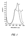
- the indium phthalocyanine pigment When deposited on a substrate maintained at room temperature, the indium phthalocyanine pigment is in a very poorly crystalline form, referred to hereinafter is the amorphous phase. Its spectral absorption is shifted bathochromically and its photosensitivity is increased by converting it to the B-phase. This can be accomplished in several ways.
- Annealing involves heating the pigment for a time within the range of 5 to 500 seconds at a temperature in the range of 200 to 300° C. Annealing can be conducted on the pigment as vacuum-sublimed, concurrent with the positioning of a charge-transport layer, if it is to be vacuum-sublimed, or subsequent to the deposition of the charge-transport layer if the latter is a material which is not degraded at the temperatures employed for annealing.
- a second technique for conversion of the indium phthalocyanine from the amorphous phase to the a-phase involves exposure of the pigment to solvent vapor.
- suitable solvents include chlorinated hydrocarbons such as dichloromethane, chloroform, dichloroethane and trichloroethane, as well as other solvents such as toluene and tetrahydrofuran.
- chlorinated hydrocarbons such as dichloromethane, chloroform, dichloroethane and trichloroethane
- other solvents such as toluene and tetrahydrofuran.
- the time and temperature of solvent-vapor exposure will depend, to some extent, upon the particular solvent selected. Generally, however, times in the range of 5 to 100 seconds and temperatures in the range of 40 to 80° C are suitable.
- Solvent-vapor treatment converts only the surface of the indium phthalocyanine layer. If it is desired to have the B-phase at multiple depths in the charge-generation layer, vacuum sublimation of the pigment can be interrupted and solvent-vapor conversion effected. This sequence can be performed once or several times.
- a third technique for converting the indium phthalocyanine pigment from the amorphous phase to the B-phase is liquid-solvent conversion.
- This techniques involves treating the pigment either on the substrate or after removal from the substrate with a suitable liquid solvent.
- Solvents identified above as being useful for solvent-vapor conversion are suitable, as are other solvents such as acetone and dioxane.
- the pigment should remain in contact with the solvent for a time from 5 to 100 seconds at a temperature of 20 to 40 0 C.
- This third technique is particularly useful when it is desired to solvent coat the indium phthalocyanine pigment or when it is desired to coat a charge-transport layer over the indium phthalocyanine layer by a solvent treatment. In such situations, conversion of the indium phthalocyanine pigment from the amorphous-phase to the a-phase occurs concurrently with the coating operation. Additionally, when the indium phthalocyanine pigment is solvent-coated by this technique, it provides a charge-generation layer which is present in the ß-phase throughout its volume.
- the charge-generation layer can have a thickness within a wide range depending upon the degree of photosensitivity desired. Thickness affects photosensitivity in two opposite ways. As thickness increases, a greater proportion of incident radiation is absorbed by the layer but there is a greater likelihood of a charge carrier being trapped and thus not contributing to image formation. Thus, these two factors must be balanced in selecting an appropriate thickness. We have found that a thickness in the range of 0.05 ⁇ m to 3.0 ⁇ m is preferred for maximum photosensitivity. At thicknesses much below 0.05 ⁇ m there is inadequate absorption of incident actinic radiation, whereas at thicknesses much above 3.0 ⁇ m there is excessive trapping of charge carriers.
- all of the indium phthalocyanine in the charge-generation layer need not be in the a-phase.
- a portion can be in the amorphous form or in another form. It is preferred, however, that at least 50 percent by volume of the indium phthalocyanine present in the charge- generation layer be in the S-phase.
- the charge-transport layer can be comprised of any material, organic or inorganic, which is capable of transporting charge carriers generated in the charge-generation layer. Most charge-transport materials preferentially accept and transport either positive charges (holes) or negative charges (electrons), although there are amphiteric materials known which will transport both positive and negative charges. Transport materials which exhibit a preference for conduction of positive charge carriers are referred to as p-type transport materials whereas those which exhibit a preference for the conduction of negative charges are referred to as n-type.
- p-type organic charge-transport materials may be used in the charge-transport layer of the present invention. Any of a variety of organic photoconductive materials which are capable of transporting positive charge carriers may be employed. Representative p-type organic photoconductive materials include:
- D and G which may be the same or different, represent aryl groups and J and E, which may be the same or different, represent a hydrogen atom, an alkyl group, or an aryl group, at least one of D, E and G containing an amino substituent.
- An especially useful polyarylalkane photoconductor which may be employed as the charge-transport material is a polyarylalkane having the formula noted above wherein J and-E represent a hydrogen atom, an aryl group or an alkyl group, and D and G represent substituted aryl groups having as a substituent thereof a group represented by the formula: wherein:
- Strong Lewis base materials such as aromatic materials, including aromatically unsaturated heterocyclic materials which are free from strong electron-withdrawing groups.
- a partial listing of such aromatic Lewis base materials includes tetraphenylpy- rene, 1-methylpyrene, perylene, chrysene, anthracene, tetraphene, 2-phenyl naphthalene, azapyrene, fluor- ene, fluorenone, 1-ethylpyrene, acetyl pyrene, 2,3-benzochrysens, 3,4-benzopyrene, 1,4-bromopyrene, phenylindole, polyvinyl carbazole, polyvinyl pyrene,
- polyvinyl tetracene polyvinyl perylene and polyvinyl tetraphene.
- p-type charge-transport materials which may be employed in the present invention are any of the p-type organic photoconductors, including metallo-organo materials, known to be useful in electrophotographic processes, such as any of the organic photoconductive materials described in Research Disclosure, Vol. 109, May, 1973, pages 61-67, paragraph IV (A) (2) through (13), which are p-type photoconductors.
- n-type charge-transport materials are strong Lewis acids such as organic, including metallo-organic, materials containing one or more aromatic, including aromatically unsaturated heterocyclic, materials bearing an electron-withdrawing substituent. These materials are considered useful because of their characteristic electron- accepting capability.
- Typical electron-withdrawing substituents include cyano and nitro groups; sulfonate groups; halogens such as chlorine, bromine and iodine; ketone groups; ester groups; acid anhydride groups; and other acid groups such as carboxyl and quinone groups.
- a partial listing of such representative n-type aromatic Lewis acid materials having electron-withdrawing substituents includes phthalic anhydride, tetrachlorophthalic anhydride, benzil, mellitic anhydride, S-tricyanobenzene, picryl chloride, 2,4-dinitrochlorobenzene, 2,4-dinitrobromoben- zene, 4-nitrobiphenyl, 4,4-dinitrobiphenyl, 2,4,6- trinitroanisole, trichlorotrinitrobenzene, trinitro- o-toluene, 4,6-dichloro-1,3-dinitrobenzene, 4,6-dibromo-1,3-dinitrobenzene, p-dinitrobenzene, chlora- nil, bromanil, 2,4,7-trinitro-9-fluorenone, 2,4,5,7-tetranitrofluorenone, trinitroanthracene, dinitroac- ridene, tetra
- n-type charge-transport materials which may be employed in the present invention are conventional n-type organic photoconductors, for example, complexes of 2,4,6-trinitro-9-fluorenone and poly(vinyl carbazole).
- Still other n-type organic, including metallo-organo, photoconductive materials useful as n-type charge-transport materials in the present invention are any of the organic photoconductive materials known to be useful in electrophotographic processes such as any of the materials described in Research Disclosure, Vol. 109, May, 1973, pages 61-67, paragraph IV(A) (2) through (13), which are n-type photoconductors.
- a single charge-transport layer can be employed, or more than one can be employed. Where a single charge-transport layer is employed, it can be either a p-type or an n-type material.
- a preferred configuration of layers is to have the charge-generation layer between the conducting support and a single charge-transport layer. Because there are a multiplicity of suitable charge-transport materials, this arrangement provides a great deal of flexibility and permits physical and surface characteristics of the element to be controlled by the nature of the charge-transport layer selected.
- the charge-generation layer be exposed to actinic radiation through the charge-transport layer
- the charge-transport layer it is preferred that the charge-transport layer have little or no absorption in the region of the electromagnetic spectrum to which the charge-generation layer responds, thus permitting the maximum amount of actinic radiation to reach the charge-generation layer. Where the charge-transport layer is not in the path of exposure, this consideration does not apply.
- Each of the charge-generation and charge-transport layers can be applied by vacuum deposition or by solvent coating.
- solvent coating is employed to coat either or all of these layers, a suitable film-forming polymeric binder material can be employed.
- the binder material may, if it is an electrically insulating material, help provide the element with electrical insulating characteristics. It also serves as a film-forming material useful in (a) coating the layer, (b) adhering the layer to an adjacent layer and (c), when it is a top layer, providing a smooth, easy-to-clean, wear-resistant surface.
- the optimum ratio of charge- generation or charge-transport material to binder material may vary widely depending on the particular polymeric binder(s) and particular charge-transport material(s) employed. In general, it has been found that, when a binder material is employed, useful results are obtained wherein the amount of active charge-generation or charge-transport material contained within the layer varies within the range of from 5 to 90 weight percent based on the dry weight of the layer.
- a partial listing of representative materials which may be employed as binders in the charge- generation and charge-transport layers includes such film-forming polymeric materials having a fairly high dielectric strength and good electrically insulating properties as styrene-butadiene copolymers; polyvinyl toluene-styrene copolymers; styrene-alkyd resins; silicone-alkyd resins; soya-alkyd resins; vinylidene , chloride-vinyl chloride copolymers; poly(vinylidene chloride); vinylidene chloride-acrylonitrile copolymers; vinyl acetate-vinyl chloride copolymers; poly-(vinyl acetals) such as poly(vinyl butyral); nitrated polystyrene; polymethylstyrene; isobutylene polymers; polyesters such as poly[ethylene-coalkylenebis(alkyl- eneoxyaryl)phenylenedica
- Heterocyclicor aromatic-containing polymers which are especially useful in p-type charge-transport layers include styrene-containing polymers, bisphenol A polycarbonate polymers, phenolformaldehyde resins, polyesters such as poly[ethylene-co-isopropylidene-2,2-bis(ethyleneoxy-phenylene)]-terephthalate, and copolymers of vinyl haloacrylates and vinylacetate such as poly(vinyl-m-bromobenzoate- co-vinyl acetate).
- the charge-generation and charge-transport layers can also contain other addenda such as level- ing agents, surfactants and plasticizers to enhance or improve various physical properties of the layer.
- various addenda to modify the electrophotographic response of the element can be incorporated in the charge-transport layer.
- various contrast-control materials such as certain hole-trapping agents and certain easily oxidized dyes, can be incorporated in the charge-transport layer.
- Various such contrast-control materials are described in Research Disclosure, Vol. 122, June, 1974, p. 33, in an article entitled "Additives For Contrast Control In Organic Photoconductor Compositions and Elements".
- the components of the layer are dissolved or dispersed in a suitable liquid, together with the binder if one is employed, and other addenda as described above.
- suitable liquids include aromatic hydrocarbons such as benzene, naphthalene, toluene, xylene and mesitylene; ketones such as acetone and butanone; halogenated hydrocarbons such as methylene chloride, chloroform and ethylene chloride; ethers including ethyl ether and cyclic ethers such as tetrahydrofuran; and mixtures of the above.
- solvent-coating techniques are to be relied upon to convert the indium phthalocyanine from the amorphous phase to the B-phase, the solvent should be one of those previously identified above as being suitable for this purpose.
- a variety of electrically conducting supports can be employed in the elements of this invention such as, for example, paper (at a relative humidity above 20 percent); aluminum-paper laminates; metal foils such as aluminum foil and zinc foil; metal plates such as aluminum, copper, zinc brass and galvanized plates; vapor-deposited metal layers such as silver, chromium, nickel and aluminum coated on paper or conventional photographic film bases such as poly(ethylene terephthalate), cellulose acetate, polystyrene, etc.
- Such conducting materials as chromium and nickel can be vacuum-deposited on transparent film supports in layers sufficiently thin o allow electrophotographic elements prepared therewith to be exposed from either side of such elements.
- An especially useful conducting support can be prepared by coating a support material such as poly(ethylene terephthalate) with a conducting layer containing a semiconductor dispersed in a resin.
- a support material such as poly(ethylene terephthalate)
- a conducting layer containing a semiconductor dispersed in a resin Such conducting layers both with and without electrical barrier layers are described in US Patent 3,245,833 by Trevoy.
- Other useful conducting layers include compositions consisting essentially of an intimate mixture of at least one protective inorganic oxide and from 30 to 70 percent by weight of at least one conducting metal, e.g., a vacuum-deposited cermet conducting layer as described by Rasch US Patent 3,880,657.
- a suitable conducting coating can be prepared from the sodium salt of a carboxyester lactone of maleic anhydride and a vinyl acetate polymer.
- Such kinds of conducting layers and methods for their optimum preparation and use are disclosed in US Patents 3,007,901 by Minsk and 3,262,807.
- the various layers of the element can be coated directly on the conducting substrate.
- Such subbing layers if used, typically have a dry thickness in the range of 0.01 to 5 microns.
- Typical subbing layer materials which may be used include film-forming polymers such as cellulose nitrate, polyesters, copolymers of poly(vinyl pyrrolidone) and vinylacetate, and various vinylidene chloride-containing polymers including two-, threeand four-component polymers prepared from a polymerizable blend of monomers or prepolymers containing at least 60 percent by weight of vinylidene chloride.
- film-forming polymers such as cellulose nitrate, polyesters, copolymers of poly(vinyl pyrrolidone) and vinylacetate
- various vinylidene chloride-containing polymers including two-, threeand four-component polymers prepared from a polymerizable blend of monomers or prepolymers containing at least 60 percent by weight of vinylidene chloride.
- a partial list of representative vinylidene chloride-containing polymers includes vinylidene chloride-methyl methacrylate-itaconic acid terpolymers as disclosed in US Patent 3,143,
- Various vinylidene chloride containing hydrosol tetrapolymers which may be used include tetrapolymers of vinylidene chloride, methyl acrylate, acrylonitrile and acrylic acid, as disclosed in US Patent 3,640,708.
- a partial listing of other useful vinylidene chloride-containing copolymers includes poly(vinylidene chloride-methyl acrylate), poly(vinylidene chloride-methacrylonitrile), poly(vinylidene chloride-acrylonitrile) and poly(vinylidene chloride-acrylonitrile-methyl acrylate).
- Other useful subbing materials include the so-called tergels which are described in Nadeau et al US Patent 3,501,301 and the vinylidine chloride terpolymers described in Nadeau US Patent 3,228,770.
- One especially useful subbing layer which can be employed in the elements of the invention ie a hydrophobic film-forming polymer or copolymer free from any acid-containing group, such as a carboxyl group, prepared from a blend of monomers or prepolymers, each of said monomers or prepolymers containing one or more polymerizable ethylenically unsaturated groups.
- a partial listing of such useful materials includes many of the above-mentioned copolymers and, in addition, the following polymers: copolymers of polyvinylpyrrolidone and vinyl acetate, and poly(vinylidene chloride-methyl methacrylate).
- Optional overcoat layers can be used in the elements of the present invention.
- the surface layer of the element of the invention can be coated with one or more electrically insulating, organic polymer coatings or electrically insulating, inorganic coatings.
- electrically insulating, organic polymer coatings or electrically insulating, inorganic coatings are well-known in the art and accordingly extended discussion thereof is unnecessary.
- Typical useful such overcoats are described for example, in Research Disclosure, "Electrophotographic Elements, Materials and Processes", Vol. 109, p. 63, Paragraph V, May, 1973.
- the photoconductive elements of this invention can be used in the ways and for the purposes that such elements are used in the art. While they will find principal use as electrophotographic elements in the art of electrophotography, they can also be used in other arts, such as the solar-cell art, where photoconductive elements are employed.
- Phthalonitrile (160 g, 1.25 M) and anhydrous indium trichloride (99% pure, 70.4 g, 0.32 M) were combined in a 500-mL, 3-neck flask and heated under nitrogen with stirring for 1 hr at 163° C, the flask being completely submerged in a salt bath. The temperature was then raised over a period of 1 hr to a final temperature of 285° C. The product was allowed to cool and solidify, was ground with a mortar and pestle, and then was slurried at room temperature in 2400 ml of toluene and 2400 ml of acetone. It was then extracted with acetone until the effluent was colorless (approximately 2 days).
- the product was recrystallized from a-chloronaphthalene.
- the solid obtained from recrystallization was extracted in a Soxhlet extractor with acetone until the effluent was colorless.
- the product was collected on a funnel and dried at 60° C overnight in a vacuum oven to yield 25.3 g of blue solid (35%).
- Characteristic bands in the infrared spectra due to the acetyl acetoxy group appear at 1580 cm -1 and 1510 cm -1 .
- chloroindium chlorophthalocyanine prepared as in preparative Example 1 were placed in a tantalum crucible (R. D. Mathis Co., Model SM-8) and mounted in a vacuum-deposition apparatus (Varian Vacuum Equipment Model 3117).
- a substrate consisting of a 10-cm x 10-cm x 2-cm hollow aluminum plate, was placed above the center of the crucible at a distance of approximately 17 cm. The substrate was cooled with liquid nitrogen.
- a shutter positioned between the crucible and the substrate at a distance of approximately 4 cm from the crucible, was placed in the closed position during evacuation and initial heating.
- the crucible After evacuation to about 13 X 10 -5 Pascal, the crucible was heated to about 200° C. At this temperature, low-temperature volatile impurities present in the chloroindium chlorophthalocyanine sublimed and condensed on the surface of the shutter. The 200°-C temperature was maintained for 5-10 min. (The exact time required for purification depends mainly on crucible size and the amount of material to be purified.)
- the temperature of the crucible was increased to about 500-520 0 C. Once this temperature was reached, the shutter was opened. A quartz crystal deposition-rate monitor, positioned adjacent the substrate, was used to indicate sublimation of chloroindium chlorophthalocyanine. After a few minutes at 500-520 0 C, deposition rates between 10-50 nm/sec were observed. Deposition was continued until the deposition rate decreased to about 1 nm/sec. The crucible was then allowed to cool to about 100° C and the vacuum removed.
- a thick film of chloroindium chlorophthalocyanine was obtained on the deposition substrate. This deposit was removed by scraping from the substrate with a sharp blade.
- Indium phthalocyanines can be converted to the ß-phase by annealing or solvent-vapor treatment. This example illustrates both techniques.
- Three elements were prepared, each comprising, in order, a nickel-coated glass substrate, a 0.2-um chloroindium chlorophthalocyanine charge- generation layer and a 10- p m 1,1-bis(4-di-p-tolyl- aminophenyl)cyclohexane charge-transport layer.
- Both the charge-generation and charge-transport layers were thermally sublimed from a tantalum crucible in a vacuum-deposition apparatus evaporator evacuated to a background pressure of 2.6 x 10 -5 Pascal.
- the glass substrate was mounted 20 cm from the crucible and was maintained at room temperature (23 0 C) throughout the deposition of both layers.
- Both layers were deposited at a rate of about 10 nm/sec, the crucible being heated to a temperature of 350° C during the deposition of the charge-generation layer and to a temperature of 200° C during the deposition of the charge-transport layer.
- individual ones of the charge-generation layers were treated as follows:
- This example illustrates the use of a solvent dispersion technique to convert the indium phthalocyanine to the ß-phase and the solvent coating of both the charge-generation and charge-transport layers.
- the charge-generation layer formulation was agitated on a paint shaker for 2 hr and then diluted with methylene chloride to 3.5% solids, filtered and coated to yield a dry thickness of l ⁇ m on a poly-(ethylene terephthalate) support.
- the charge-transport layer formulation was coated over the charge-generation layer to yield a dry thickness of 10 p m.
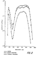
- the xerographic sensitivity of the element, measured as in Test Example 2, is shown in Figure 3. It will be noted that the material shows good sensitivity out to 900 nm.
- indium phthalocyanines The high sensitivity of indium phthalocyanines is obtained only with the combination of a ß-phase layer electrically contiguous a charge-transport layer.
- two 1.0 ⁇ m single-layer control elements of chloroindium chlorophthalocyanine were prepared. Control 1 was not treated afterward. Control 2 was exposed to dichloromethane vapor for 5 sec. In an element according to this invention, a 0.2pm chloroindium chlorophthalocyanine charge-generation layer was exposed to dichloromethane vapor for 1 hr and then a 17 ⁇ m transport layer of 1,1-bis(4-di-p-tolylaminophenyl)-cyclohexane was vacuum-sublimed thereover.
- Quantum efficiency is defined as the ratio of the decrease of the surface charge density to the incident photon flux, assuming charge density is related to surface voltage by the geometrical capacitance. Defined in this manner, the maximum efficiency is unity.
- the potential discharge measurements were made at 810 nm with an electric field of 8 x 10 4 V/cm.
- a series of elements was prepared, each having a different phthalocyanine charge-generation layer.
- the elements had the following layers, in order: a nickel-coated, poly(ethylene terephthalate) support, a polyester blocking layer, a 0.2vm charge- generation layer and a 10mm charge-transport layer.
- the charge-generation layer was composed of one of the phthalocyanines, identified below, vacuum-sublimed from a tantalum crucible at a temperature of 350° C and a background pressure of 2 X 10 -3 Pascal.
- the charge-transport layer was composed of tri-p-tolylamine in bisphenol A polycarbonate coated from a solvent mixture of methylene chloride and 1,1,2-trichloroethane.
- Table III reports the xerographic exposure (E x ) required to discharge a corona-charged element from 500 to 100 volts at wavelengths of 810 and 850 nm.
- the charge-generation layer was a 0.2 ⁇ m layer of chloroindium chlorophthalocyanine prepared by vacuum sublimation as in Example 1. All solvent-vapor exposures were for 60 minutes. After solvent-vapor exposure, a 10 p m transport layer of 1,1-bis(4-di-p-tolylaminophenyl)cyclohexane was vacuum-deposited over the charge-generation layer.
- the length of solvent-vapor exposure can be varied widely, as illustrated in Table IV.
- the measurements were made using elements as described in Example 6 which had been solvent-vapor-treated with tetrahydrofuran for the time indicated in the table.
- a 0.1 ⁇ m film element containing a chloroindium chlorophthalocyanine was formed by vacuum deposition using the procedures described in Example 1. This initial layer was removed from vacuum and subjected to dichloromethane vapor treatment for about 30 min. This procedure was repeated two additional times, giving a 0.3 ⁇ m thick charge-generation layer composed of three stacked 0.1 ⁇ m layers, the free surface of each layer having been solvent converted. A 17pm transport layer of 1,1-bia(4-di-p-tolylamino- phenyl)cyclohexane was then vacuum-deposited over the multilayer emitter structure.
Abstract
Description
- This invention relates to photoconductive elements.
- Photoconductive materials have been described as materials having the ability to generate mobile charge carriers as a result of exposure to actinic radiation and to transport them through the bulk of the material. This property has formed the basis for the art of electrophotography and finds use in other technologies, such as solar cells.
- Photoconductive elements comprise a conducting support bearing a layer of a photoconductive material which is insulating in the dark but which becomes conductive upon exposure to actinic radiation. A common technique for forming images with such elements is uniformly electrostatically to charge the surface of the element and then imagewise- expose it to actinic radiation. In areas where the photoconductive layer is irradiated, mobile charge carriers are generated which migrate to the surface of the element and there dissipate the surface charge. This leaves behind a charge pattern in nonirradiated areas, referred to as a latent electrostatic image. This latent electrostatic image can then be developed, either on the surface on which it is formed or on another surface to which it has been transferred, by application of a liquid or dry developer composition which contains finely divided electroscopic marking particles which either are selectively attracted to and deposit in the charged areas or are repelled by the charged areas and selectively deposited in the uncharged areas. The pattern of marking particles can be fixed to the surface on which they are deposited or they can be transferred to another surface and fixed there.
- Numerous photoconductive materials have been described as being useful in electrophotography. These include inorganic materials, the best known of which are selenium and zinc oxide, as well as organic materials, both monomeric and polymeric, such as arylamines, arylmethanes, azoles, carbazoles, pyrroles and phthalocyanines.
- Electrophotographic elements can comprise a single active layer, containing the photoconductive material, or they can comprise multiple active layers. Elements with multiple active layers (sometimes referred to as multiactive elements) have at least one charge-generation layer and at least one charge-transport layer. The charge-generation layer responds to actinic radiation by generating mobile charge carriers and the charge-transport layer facilitates migration of the charge carriers to the surface of the element where they dissipate the uniform electrostatic charge and thus form the latent electrostatic image.
- The majority of photoconductors described in the art are sensitive to electromagnetic radiation in the ultraviolet and visible regions of the electromagnetic spectrum. However, as information-storage and -retrieval technology has evolved, increasing use has been made of diode lasers, light-emitting devices which emit radiation principally in the near infrared region of the electromagnetic spectrum, i.e., from 700 nm to 900 nm. Known photoconductive materials either do not adequately respond to radiation in this region of the spectrum, i.e., they have little or no sensitivity to such radiation, or, if they do respond to such radiation, they suffer from other disadvantages. For example, they may have very high dark conductivities which limit their ability to accept and hold an electrostatic charge, or they may have poor quantum efficiencies which prevent them from making effective use of exposing radiation and result in low electrophotographic sensitivity, or they may require the application of an extremely high electrostatic charge or the use of other extreme conditions in order to exhibit useful electrophotographic sensitivity.
- The object of the invention is to provide a photoconductive element comprising an electrically conductive support, a charge-generation layer and a charge-transport layer which has high electrophotographic sensitivity in the near infrared region of the electromagnetic spectrum.
- This object has been achieved with an element having the above features which is characterized in that the charge-generation layer comprises the B-phase of an indiumphthalocyanine pigment.
- Multiactive photoconductive elements of the invention containing a B-phase indium phthalocyanine chargegeneration layer, in addition to exhibiting high electrophotographic sensitivity, exhibit high charge acceptance, low dark decay and high quantum efficiency. This is unexpected because, although phthalocyanine pigments in general have been known to be electrically photosensitive (see, for example, US Patents 3,903,107 and 3,615,558), the unique combination of high infrared photosensitivity, high charge acceptance, low dark decay and high quantum efficiency of multiactive elements containing a a-phase indium phthalocyanine has not been recognized.
- Indium phthalocyanines useful in this invention can be unsubstituted or can have substituents associated with the indium atom, the phthalocyanine ring, or both. Preferred substituents, for either or both of the indium atom and the phthalocyanine ring, are halogen atoms such as fluorine, chlorine, bromine and iodine. Other substituents which can be associated with the indium atom are hydroxy, alkoxy, aryloxy, alkylcarbonyloxy, arylcarbonyloxy, siloxy, oxyindium phthalocyanine and acetylacetonate. Other substituents which can be associated with the phthalocyanine ring are alkyl, alkoxy, aryl, aryloxy and fused aromatic carbocylic or nitrogen-containing heterocyclic rings. The alkyl substituents, as well as the alkyl portion of the alkoxy and alkylcarbonyloxy substituents, can contain 1 to 22 carbon atoms. The aryl substituents, as well as the aryl portion of the aryloxy and arylcarbonyloxy substituents, can contain 6 to 22 carbon atoms.
- Especially preferred indium phthalocyanines contain chlorine substituents on either or both of the indium atom and the phthalocyanine ring. Thus, especially preferred are chloroindium phthalocyanine, indium chlorophthalocyanine, chloroindium chlorophthalocyanine and mixtures thereof.
- Preferred materials can be represented by the structural formula:

- each of X and Y is halogen, preferably chlorine or bromine;
- m is 0 to 16; and
- n is 0 or 1.
- Indium phthalocyanines can be prepared by procedures known in the art. Halogen-substituted indium phthalocyanines can be prepared by techniques described by G. P. Shaposhnikov, et al., Izv. Vyssh. Uchebn, Zaved., Khim. Khim. Tekhnol, 1977, 20 (2), 184-6; D. Colaitis, Bull. Soc. Chim., p. 23 (1962); and P. Muehl, Krist. Tech., 1965, 2 (3), 431-5. Representative preparations are shown in the preparative examples hereinafter.
- As prepared by these techniques, the indium phthalocyanines are in the ß-phase. The photoconductive properties of the materials can be improved by removal of impurities. A preferred purification technique is vacuum sublimation. This technique is especially useful with the halogen-substituted indium phthalocyanines and similar materials which do not undergo significant decomposition at sublimation temperatures. For other materials, known purification techniques can be employed which do not heat the material to a temperature at which significant decomposition occurs. Some purification techniques convert the indium phthalocyanine pigment from the preferred S-phase to another form. In that event, the pigment can be converted back to the B-phase by annealing techniques which will be described in more detail hereinafter.
- Vacuum sublimation can be effected by placing the indium phthalocyanine pigment in a crucible contained in a vacuum-deposition apparatus and positioning a substrate relative to the crucible so that pigment subliming from the crucible will be deposited upon the substrate. The vacuum chamber is preferably maintained at a background pressure of between 10-3 and 10 5 Pascal. The crucible is heated to the minimum temperature consistent with an adequate rate of sublimation of the pigment. Temperatures in the range of 300 to 400°C are preferred. It is preferred that the substrate be maintained at a temperature close to room temperature. This can be accomplished by positioning the substrate sufficiently far from the crucible that it is not heated, or by cooling the substrate.
- If the pigment contains impurities which are volatile at temperatures below that at which the pigment sublimes, they can be removed by interposing a shutter between the substrate and the crucible and heating the crucible to a temperature below that at which significant sublimation of the indium phthalocyanine pigment occurs. A temperature in the range of 200 to 250°C is often suitable. After the impurities have been deposited on the shutter, the shutter is removed and the temperature raised to sublime the pigment onto the substrate.
- When deposited on a substrate maintained at room temperature, the indium phthalocyanine pigment is in a very poorly crystalline form, referred to hereinafter is the amorphous phase. Its spectral absorption is shifted bathochromically and its photosensitivity is increased by converting it to the B-phase. This can be accomplished in several ways.
- One technique is annealing. This involves heating the pigment for a time within the range of 5 to 500 seconds at a temperature in the range of 200 to 300° C. Annealing can be conducted on the pigment as vacuum-sublimed, concurrent with the positioning of a charge-transport layer, if it is to be vacuum-sublimed, or subsequent to the deposition of the charge-transport layer if the latter is a material which is not degraded at the temperatures employed for annealing.
- A second technique for conversion of the indium phthalocyanine from the amorphous phase to the a-phase involves exposure of the pigment to solvent vapor. Suitable solvents include chlorinated hydrocarbons such as dichloromethane, chloroform, dichloroethane and trichloroethane, as well as other solvents such as toluene and tetrahydrofuran. The time and temperature of solvent-vapor exposure will depend, to some extent, upon the particular solvent selected. Generally, however, times in the range of 5 to 100 seconds and temperatures in the range of 40 to 80° C are suitable.
- Solvent-vapor treatment converts only the surface of the indium phthalocyanine layer. If it is desired to have the B-phase at multiple depths in the charge-generation layer, vacuum sublimation of the pigment can be interrupted and solvent-vapor conversion effected. This sequence can be performed once or several times.
- A third technique for converting the indium phthalocyanine pigment from the amorphous phase to the B-phase is liquid-solvent conversion. This techniques involves treating the pigment either on the substrate or after removal from the substrate with a suitable liquid solvent. Solvents identified above as being useful for solvent-vapor conversion are suitable, as are other solvents such as acetone and dioxane. The pigment should remain in contact with the solvent for a time from 5 to 100 seconds at a temperature of 20 to 400 C.
- This third technique is particularly useful when it is desired to solvent coat the indium phthalocyanine pigment or when it is desired to coat a charge-transport layer over the indium phthalocyanine layer by a solvent treatment. In such situations, conversion of the indium phthalocyanine pigment from the amorphous-phase to the a-phase occurs concurrently with the coating operation. Additionally, when the indium phthalocyanine pigment is solvent-coated by this technique, it provides a charge-generation layer which is present in the ß-phase throughout its volume.
- As coated, either by vacuum sublimation or by solvent coating, the charge-generation layer can have a thickness within a wide range depending upon the degree of photosensitivity desired. Thickness affects photosensitivity in two opposite ways. As thickness increases, a greater proportion of incident radiation is absorbed by the layer but there is a greater likelihood of a charge carrier being trapped and thus not contributing to image formation. Thus, these two factors must be balanced in selecting an appropriate thickness. We have found that a thickness in the range of 0.05µm to 3.0µm is preferred for maximum photosensitivity. At thicknesses much below 0.05µm there is inadequate absorption of incident actinic radiation, whereas at thicknesses much above 3.0µm there is excessive trapping of charge carriers.
- As suggested above in connection with the conversion of the indium phthalocyanine pigment from the amorphous-phase to the B-phase, all of the indium phthalocyanine in the charge-generation layer need not be in the a-phase. A portion can be in the amorphous form or in another form. It is preferred, however, that at least 50 percent by volume of the indium phthalocyanine present in the charge- generation layer be in the S-phase.
- The charge-transport layer can be comprised of any material, organic or inorganic, which is capable of transporting charge carriers generated in the charge-generation layer. Most charge-transport materials preferentially accept and transport either positive charges (holes) or negative charges (electrons), although there are amphiteric materials known which will transport both positive and negative charges. Transport materials which exhibit a preference for conduction of positive charge carriers are referred to as p-type transport materials whereas those which exhibit a preference for the conduction of negative charges are referred to as n-type.
- Various p-type organic charge-transport materials may be used in the charge-transport layer of the present invention. Any of a variety of organic photoconductive materials which are capable of transporting positive charge carriers may be employed. Representative p-type organic photoconductive materials include:
- 1. Carbazole materials including carbazole, N-ethyl carbazole, N-isopropyl carbazole, N-phenyl carbazole, halogenated carbazoles, and various polymeric carbazole materials such as poly(vinyl carbazole) halogenated poly(vinyl carbazole).
- 2. Arylamine-containing materials including mono- arylamines, diarylamines and triarylamines, as well as polymeric arylamines. A partial listing of specific arylamine organic photoconductors include the nonpolymeric triphenylamines illustrated by Klupfel et al US Patent 3,180,730; the polymeric triarylamines described by Fox US Patent 3,240,597; the triarylamines having at least one of the aryl radicals substituted by either a vinyl radical or a vinylene radical having at least one active hydrogencontaining group, as described by Brantly et al US Patent 3,567,450; the triarylamines in which at least one of the aryl radicals is substituted by an active hydrogen-containing group, as described by Brantly et al US Patent 3,658,520; and tritolylamine.
- 3. Polyarylalkane materials of the type described by Noe et al US Patent 3,274,000, Wilson US Patent 3,542,547, and Rule et al U.S. Patent No. 3,615,402. Preferred polyarylalkane photoconductors can be represented by the formula:

- D and G, which may be the same or different, represent aryl groups and J and E, which may be the same or different, represent a hydrogen atom, an alkyl group, or an aryl group, at least one of D, E and G containing an amino substituent. An especially useful polyarylalkane photoconductor which may be employed as the charge-transport material is a polyarylalkane having the formula noted above wherein J and-E represent a hydrogen atom, an aryl group or an alkyl group, and D and G represent substituted aryl groups having as a substituent thereof a group represented by the formula:

- R represents an unsubstituted aryl group such as phenyl or an alkyl-substituted aryl such as a tolyl group. Additional information concerning certain of these latter polyarylalkanes may be found in Rule et al US Patent 4,127,412.
- 4. Strong Lewis base materials such as aromatic materials, including aromatically unsaturated heterocyclic materials which are free from strong electron-withdrawing groups. A partial listing of such aromatic Lewis base materials includes tetraphenylpy- rene, 1-methylpyrene, perylene, chrysene, anthracene, tetraphene, 2-phenyl naphthalene, azapyrene, fluor- ene, fluorenone, 1-ethylpyrene, acetyl pyrene, 2,3-benzochrysens, 3,4-benzopyrene, 1,4-bromopyrene, phenylindole, polyvinyl carbazole, polyvinyl pyrene,
- polyvinyl tetracene, polyvinyl perylene and polyvinyl tetraphene.
- 5. Other useful p-type charge-transport materials which may be employed in the present invention are any of the p-type organic photoconductors, including metallo-organo materials, known to be useful in electrophotographic processes, such as any of the organic photoconductive materials described in Research Disclosure, Vol. 109, May, 1973, pages 61-67, paragraph IV (A) (2) through (13), which are p-type photoconductors.
- Representative of n-type charge-transport materials are strong Lewis acids such as organic, including metallo-organic, materials containing one or more aromatic, including aromatically unsaturated heterocyclic, materials bearing an electron-withdrawing substituent. These materials are considered useful because of their characteristic electron- accepting capability. Typical electron-withdrawing substituents include cyano and nitro groups; sulfonate groups; halogens such as chlorine, bromine and iodine; ketone groups; ester groups; acid anhydride groups; and other acid groups such as carboxyl and quinone groups. A partial listing of such representative n-type aromatic Lewis acid materials having electron-withdrawing substituents includes phthalic anhydride, tetrachlorophthalic anhydride, benzil, mellitic anhydride, S-tricyanobenzene, picryl chloride, 2,4-dinitrochlorobenzene, 2,4-dinitrobromoben- zene, 4-nitrobiphenyl, 4,4-dinitrobiphenyl, 2,4,6- trinitroanisole, trichlorotrinitrobenzene, trinitro- o-toluene, 4,6-dichloro-1,3-dinitrobenzene, 4,6-dibromo-1,3-dinitrobenzene, p-dinitrobenzene, chlora- nil, bromanil, 2,4,7-trinitro-9-fluorenone, 2,4,5,7-tetranitrofluorenone, trinitroanthracene, dinitroac- ridene, tetracyanopyrene, dinitroanthraquinone, and mixtures thereof.
- Other useful n-type charge-transport materials which may be employed in the present invention are conventional n-type organic photoconductors, for example, complexes of 2,4,6-trinitro-9-fluorenone and poly(vinyl carbazole). Still other n-type organic, including metallo-organo, photoconductive materials useful as n-type charge-transport materials in the present invention are any of the organic photoconductive materials known to be useful in electrophotographic processes such as any of the materials described in Research Disclosure, Vol. 109, May, 1973, pages 61-67, paragraph IV(A) (2) through (13), which are n-type photoconductors.
- A single charge-transport layer can be employed, or more than one can be employed. Where a single charge-transport layer is employed, it can be either a p-type or an n-type material.
- A preferred configuration of layers is to have the charge-generation layer between the conducting support and a single charge-transport layer. Because there are a multiplicity of suitable charge-transport materials, this arrangement provides a great deal of flexibility and permits physical and surface characteristics of the element to be controlled by the nature of the charge-transport layer selected.
- Where it is intended that the charge- generation layer be exposed to actinic radiation through the charge-transport layer, it is preferred that the charge-transport layer have little or no absorption in the region of the electromagnetic spectrum to which the charge-generation layer responds, thus permitting the maximum amount of actinic radiation to reach the charge-generation layer. Where the charge-transport layer is not in the path of exposure, this consideration does not apply.
- Each of the charge-generation and charge-transport layers can be applied by vacuum deposition or by solvent coating. When solvent coating is employed to coat either or all of these layers, a suitable film-forming polymeric binder material can be employed. The binder material may, if it is an electrically insulating material, help provide the element with electrical insulating characteristics. It also serves as a film-forming material useful in (a) coating the layer, (b) adhering the layer to an adjacent layer and (c), when it is a top layer, providing a smooth, easy-to-clean, wear-resistant surface.
- Where a polymeric binder material is employed in either the charge-generation or charge-transport layer, the optimum ratio of charge- generation or charge-transport material to binder material may vary widely depending on the particular polymeric binder(s) and particular charge-transport material(s) employed. In general, it has been found that, when a binder material is employed, useful results are obtained wherein the amount of active charge-generation or charge-transport material contained within the layer varies within the range of from 5 to 90 weight percent based on the dry weight of the layer.
- A partial listing of representative materials which may be employed as binders in the charge- generation and charge-transport layers includes such film-forming polymeric materials having a fairly high dielectric strength and good electrically insulating properties as styrene-butadiene copolymers; polyvinyl toluene-styrene copolymers; styrene-alkyd resins; silicone-alkyd resins; soya-alkyd resins; vinylidene , chloride-vinyl chloride copolymers; poly(vinylidene chloride); vinylidene chloride-acrylonitrile copolymers; vinyl acetate-vinyl chloride copolymers; poly-(vinyl acetals) such as poly(vinyl butyral); nitrated polystyrene; polymethylstyrene; isobutylene polymers; polyesters such as poly[ethylene-coalkylenebis(alkyl- eneoxyaryl)phenylenedicarboxylate]; phenolformaldehyde resins; ketone resins; polyamides; polycarbonates, polythiocarbonates; poly[ethylene-co-isopropylidene-2,2-bis(ethyleneoxyphenylene)terephthalate]; copolymers of vinyl haloacrylates and vinyl acetate such as poly(vinyl-m-bromobenzoate-co-vinyl acetate); and chlorinated poly(olefins) such as chlorinated poly(ethylene).
- In general, it has been found that polymers containing aromatic or heterocyclic groups are most effective as the binder materials because these polymers, by virtue of their heterocyclic or aromatic groups, tend to provide little or no interference with the transport of charge carriers through the layer. Heterocyclicor aromatic-containing polymers which are especially useful in p-type charge-transport layers include styrene-containing polymers, bisphenol A polycarbonate polymers, phenolformaldehyde resins, polyesters such as poly[ethylene-co-isopropylidene-2,2-bis(ethyleneoxy-phenylene)]-terephthalate, and copolymers of vinyl haloacrylates and vinylacetate such as poly(vinyl-m-bromobenzoate- co-vinyl acetate).
- The charge-generation and charge-transport layers can also contain other addenda such as level- ing agents, surfactants and plasticizers to enhance or improve various physical properties of the layer. In addition, various addenda to modify the electrophotographic response of the element can be incorporated in the charge-transport layer. For example, various contrast-control materials, such as certain hole-trapping agents and certain easily oxidized dyes, can be incorporated in the charge-transport layer. Various such contrast-control materials are described in Research Disclosure, Vol. 122, June, 1974, p. 33, in an article entitled "Additives For Contrast Control In Organic Photoconductor Compositions and Elements".
- When the charge-generation layer or the charge-transport layer is solvent-coated, the components of the layer are dissolved or dispersed in a suitable liquid, together with the binder if one is employed, and other addenda as described above. Useful liquids include aromatic hydrocarbons such as benzene, naphthalene, toluene, xylene and mesitylene; ketones such as acetone and butanone; halogenated hydrocarbons such as methylene chloride, chloroform and ethylene chloride; ethers including ethyl ether and cyclic ethers such as tetrahydrofuran; and mixtures of the above. Where solvent-coating techniques are to be relied upon to convert the indium phthalocyanine from the amorphous phase to the B-phase, the solvent should be one of those previously identified above as being suitable for this purpose.
- A variety of electrically conducting supports can be employed in the elements of this invention such as, for example, paper (at a relative humidity above 20 percent); aluminum-paper laminates; metal foils such as aluminum foil and zinc foil; metal plates such as aluminum, copper, zinc brass and galvanized plates; vapor-deposited metal layers such as silver, chromium, nickel and aluminum coated on paper or conventional photographic film bases such as poly(ethylene terephthalate), cellulose acetate, polystyrene, etc. Such conducting materials as chromium and nickel can be vacuum-deposited on transparent film supports in layers sufficiently thin o allow electrophotographic elements prepared therewith to be exposed from either side of such elements. An especially useful conducting support can be prepared by coating a support material such as poly(ethylene terephthalate) with a conducting layer containing a semiconductor dispersed in a resin. Such conducting layers both with and without electrical barrier layers are described in US Patent 3,245,833 by Trevoy. Other useful conducting layers include compositions consisting essentially of an intimate mixture of at least one protective inorganic oxide and from 30 to 70 percent by weight of at least one conducting metal, e.g., a vacuum-deposited cermet conducting layer as described by Rasch US Patent 3,880,657. Likewise, a suitable conducting coating can be prepared from the sodium salt of a carboxyester lactone of maleic anhydride and a vinyl acetate polymer. Such kinds of conducting layers and methods for their optimum preparation and use are disclosed in US Patents 3,007,901 by Minsk and 3,262,807.
- The various layers of the element can be coated directly on the conducting substrate. In some cases, it may be desirable to use one or more intermediate subbing layers over the conducting substrate to improve adhesion between the conducting substrate and overlying layers or to act as an electrical barrier layer between the overlying layers and the conducting substrate, as described in Dessauer US Patent 2,940,348. Such subbing layers, if used, typically have a dry thickness in the range of 0.01 to 5 microns. Typical subbing layer materials which may be used include film-forming polymers such as cellulose nitrate, polyesters, copolymers of poly(vinyl pyrrolidone) and vinylacetate, and various vinylidene chloride-containing polymers including two-, threeand four-component polymers prepared from a polymerizable blend of monomers or prepolymers containing at least 60 percent by weight of vinylidene chloride. A partial list of representative vinylidene chloride-containing polymers includes vinylidene chloride-methyl methacrylate-itaconic acid terpolymers as disclosed in US Patent 3,143,421. Various vinylidene chloride containing hydrosol tetrapolymers which may be used include tetrapolymers of vinylidene chloride, methyl acrylate, acrylonitrile and acrylic acid, as disclosed in US Patent 3,640,708. A partial listing of other useful vinylidene chloride-containing copolymers includes poly(vinylidene chloride-methyl acrylate), poly(vinylidene chloride-methacrylonitrile), poly(vinylidene chloride-acrylonitrile) and poly(vinylidene chloride-acrylonitrile-methyl acrylate). Other useful subbing materials include the so-called tergels which are described in Nadeau et al US Patent 3,501,301 and the vinylidine chloride terpolymers described in Nadeau US Patent 3,228,770.
- One especially useful subbing layer which can be employed in the elements of the invention ie a hydrophobic film-forming polymer or copolymer free from any acid-containing group, such as a carboxyl group, prepared from a blend of monomers or prepolymers, each of said monomers or prepolymers containing one or more polymerizable ethylenically unsaturated groups. A partial listing of such useful materials includes many of the above-mentioned copolymers and, in addition, the following polymers: copolymers of polyvinylpyrrolidone and vinyl acetate, and poly(vinylidene chloride-methyl methacrylate).
- Optional overcoat layers can be used in the elements of the present invention. For example, to improve surface hardness and resistance to abrasion, the surface layer of the element of the invention can be coated with one or more electrically insulating, organic polymer coatings or electrically insulating, inorganic coatings. A number of such coatings are well-known in the art and accordingly extended discussion thereof is unnecessary. Typical useful such overcoats are described for example, in Research Disclosure, "Electrophotographic Elements, Materials and Processes", Vol. 109, p. 63, Paragraph V, May, 1973.
- The photoconductive elements of this invention can be used in the ways and for the purposes that such elements are used in the art. While they will find principal use as electrophotographic elements in the art of electrophotography, they can also be used in other arts, such as the solar-cell art, where photoconductive elements are employed.
- The following examples further illustrate the invention.
- Preparation of Chloroindium Chlorophthalocyanine
- Phthalonitrile (160 g, 1.25 M) and anhydrous indium trichloride (99% pure, 70.4 g, 0.32 M) were combined in a 500-mL, 3-neck flask and heated under nitrogen with stirring for 1 hr at 163° C, the flask being completely submerged in a salt bath. The temperature was then raised over a period of 1 hr to a final temperature of 285° C. The product was allowed to cool and solidify, was ground with a mortar and pestle, and then was slurried at room temperature in 2400 ml of toluene and 2400 ml of acetone. It was then extracted with acetone until the effluent was colorless (approximately 2 days). The product was slurried 3 times wih 2400 ml of distilled water, then with 2400 ml of acetone and then was dried in a vacuum oven at 114° C overnight. Yield: 116.8 g, equivalent to 57X. Analyses were as follows:
- 1. Absorption Spectrum: See Figure 1. In this Figure, the curve labelled "1" is the absorption spectrum for the material freshly sublimed as in Example 1 infra, while that labelled "2" is the absorption spectrum for the material after annealing for 5 sec at 300° C.
- 2. Mass Spectral Analysis
- 499 unidentified
- 514 PcH2
- 548 ClPcH2
- 662 ClInPc MAJOR PEAK
- 696 ClInClPc
- 730 ClInCl2Pc
- 3. Elemental Analysis ClInCl(.67)Pc:

- 4. Water Analysis:
- 0.2%
- 51.2 g (0.40 M) phthalonitrile, 41.2 g (0.15 M) indium triacetylacetonate and 60.8 g (0.40 M) 1,8-diazabicyclo[5.4.0] undec-7-ene were added to a flask containing 2000 ml dry ethanol. The mixture was heated at reflux under a nitrogen atmosphere for 24 hr. The hot solution was filtered through a medium-porosity sintered glass funnel. The solid was washed by slurrying once with ethanol and once with water and extracted in a Soxhlet extractor with acetone until the effluent was colorless. The product was collected on a funnel and dried at 114° C overnight in a vacuum oven. The product was recrystallized from a-chloronaphthalene. The solid obtained from recrystallization was extracted in a Soxhlet extractor with acetone until the effluent was colorless. The product was collected on a funnel and dried at 60° C overnight in a vacuum oven to yield 25.3 g of blue solid (35%).
- Elemental analysis calculated for:
- C37H23N8O2In (726) C, 61.2;
- H, 3.2; N,15.4; 0, 4.4; In, 15.8
- Found: C, 61.2; H, 3.2; N, 15.4; 0, 5.8;In; 16.9 M.W. determined by field desorption mass spectrometry is 726.
- Characteristic bands in the infrared spectra due to the acetyl acetoxy group appear at 1580 cm-1 and 1510 cm-1.
- Preparation of TriphenylsiloxyIndiumphthalocyanine
- 1 g (1.38 X 10⁻³M) acetylacetonatoindium- phthalocyanine and 0.76 g (2.76 X 10-'M) triphenyl silanol were added to a flask containing 50 ml of toluene and the reaction mixture was heated at reflux for 17 hr. The hot reaction mixture was filtered through a medium-porosity sintered glass funnel and was washed by slurrying with acetone. The product was dried at 114° C overnight in a vacuum oven to yield 0.9 g of a blue solid 72X. M.W. determined by field desorption mass spectrometry 902. Infrared spectrum of product contains band at 700 cm-1 which is characteristic of the out-of-plane bending of C-H bonds in substituted benzene. Preparative Example 4
- 1 g (1.38 X 10⁻³M) acetylacetonatoindium- phthalocyanine, was added to a flask containing 48 ml glacial acetic acid and 2 ml of water. The reaction mixture was heated at reflux for 17 hr and was filtered while still hot through a medium-porosity sintered glass funnel. The solid was washed once with methanol, twice with water, and finally once with methanol, before being dried in a vacuum oven at 114° C overnight. 0.45 (481) of blue solid was obtained. Field desorption mass spectrum shows molecular weight to be 686 band in the infrared spectrum characteristic of the acetoxy group found at 1405 cm-1.
- About 2 to 3 g of chloroindium chlorophthalocyanine prepared as in preparative Example 1 were placed in a tantalum crucible (R. D. Mathis Co., Model SM-8) and mounted in a vacuum-deposition apparatus (Varian Vacuum Equipment Model 3117). A substrate, consisting of a 10-cm x 10-cm x 2-cm hollow aluminum plate, was placed above the center of the crucible at a distance of approximately 17 cm. The substrate was cooled with liquid nitrogen. A shutter, positioned between the crucible and the substrate at a distance of approximately 4 cm from the crucible, was placed in the closed position during evacuation and initial heating.
- After evacuation to about 13 X 10-5 Pascal, the crucible was heated to about 200° C. At this temperature, low-temperature volatile impurities present in the chloroindium chlorophthalocyanine sublimed and condensed on the surface of the shutter. The 200°-C temperature was maintained for 5-10 min. (The exact time required for purification depends mainly on crucible size and the amount of material to be purified.)
- Next, the temperature of the crucible was increased to about 500-5200 C. Once this temperature was reached, the shutter was opened. A quartz crystal deposition-rate monitor, positioned adjacent the substrate, was used to indicate sublimation of chloroindium chlorophthalocyanine. After a few minutes at 500-5200 C, deposition rates between 10-50 nm/sec were observed. Deposition was continued until the deposition rate decreased to about 1 nm/sec. The crucible was then allowed to cool to about 100° C and the vacuum removed.
- A thick film of chloroindium chlorophthalocyanine was obtained on the deposition substrate. This deposit was removed by scraping from the substrate with a sharp blade.
- Indium phthalocyanines can be converted to the ß-phase by annealing or solvent-vapor treatment. This example illustrates both techniques.
- Three elements were prepared, each comprising, in order, a nickel-coated glass substrate, a 0.2-um chloroindium chlorophthalocyanine charge- generation layer and a 10-pm 1,1-bis(4-di-p-tolyl- aminophenyl)cyclohexane charge-transport layer. Both the charge-generation and charge-transport layers were thermally sublimed from a tantalum crucible in a vacuum-deposition apparatus evaporator evacuated to a background pressure of 2.6 x 10⁻⁵ Pascal. The glass substrate was mounted 20 cm from the crucible and was maintained at room temperature (230 C) throughout the deposition of both layers. Both layers were deposited at a rate of about 10 nm/sec, the crucible being heated to a temperature of 350° C during the deposition of the charge-generation layer and to a temperature of 200° C during the deposition of the charge-transport layer. During the preparation of the elements, individual ones of the charge-generation layers were treated as follows:
- 1. Control - the charge-generation layer was not intentionally heated or solvent-exposed prior to the deposition of the transport layer.
- 2. Solvent converted - the charge-generation layer was exposed to dichloromethane vapor for 60 min at room temperature prior to the deposition of the transport layer.
- 3. Thermally converted - the charge-generation layer was heated to 300° C in air for 5 sec prior to the deposition of the transport layer.
- The results of potential discharge measurements on each of the elements of the invention and the control element are illustrated in Figure 2. The data are expressed as xerographic sensitivity which is defined as the reciprocal of the energy (in ergs/cm ) to discharge a corona-charged photoreceptor from 500 to 300 volts.
- Observations of these data indicate that:
- 1. The magnitude of the sensitivity of the solvent-converted sample is equivalent to the thermally converted sample and approximately a factor of 2 greater than the control.
- 2. Relative to the control, the long wavelength edge of the action spectra of the solvent or thermally converted sample is shifted-to longer wavelengths by about 60 nm.
- This example illustrates the use of a solvent dispersion technique to convert the indium phthalocyanine to the ß-phase and the solvent coating of both the charge-generation and charge-transport layers.
-

- 5.25 g Bisphenol A polycarbonate n - 2.7 120.0 g methylene chloride 78.0 g 1,1,2-trichloroethane Charge-Transport Layer

- The charge-generation layer formulation was agitated on a paint shaker for 2 hr and then diluted with methylene chloride to 3.5% solids, filtered and coated to yield a dry thickness of lµm on a poly-(ethylene terephthalate) support.
- The charge-transport layer formulation was coated over the charge-generation layer to yield a dry thickness of 10 pm. The xerographic sensitivity of the element, measured as in Test Example 2, is shown in Figure 3. It will be noted that the material shows good sensitivity out to 900 nm.
- The high sensitivity of indium phthalocyanines is obtained only with the combination of a ß-phase layer electrically contiguous a charge-transport layer. To illustrate this, two 1.0µm single-layer control elements of chloroindium chlorophthalocyanine were prepared. Control 1 was not treated afterward. Control 2 was exposed to dichloromethane vapor for 5 sec. In an element according to this invention, a 0.2pm chloroindium chlorophthalocyanine charge-generation layer was exposed to dichloromethane vapor for 1 hr and then a 17µm transport layer of 1,1-bis(4-di-p-tolylaminophenyl)-cyclohexane was vacuum-sublimed thereover. Each element was employed on a poly(ethylene terephthalate) support. In Table I, the results of a series of potential discharge measurements made with the elements are summarized. Quantum efficiency is defined as the ratio of the decrease of the surface charge density to the incident photon flux, assuming charge density is related to surface voltage by the geometrical capacitance. Defined in this manner, the maximum efficiency is unity. The potential discharge measurements were made at 810 nm with an electric field of 8 x 10⁴ V/cm.

- A series of elements was prepared, each having a different phthalocyanine charge-generation layer. The elements had the following layers, in order: a nickel-coated, poly(ethylene terephthalate) support, a polyester blocking layer, a 0.2vm charge- generation layer and a 10mm charge-transport layer. The charge-generation layer was composed of one of the phthalocyanines, identified below, vacuum-sublimed from a tantalum crucible at a temperature of 350° C and a background pressure of 2 X 10⁻³ Pascal. The charge-transport layer was composed of tri-p-tolylamine in bisphenol A polycarbonate coated from a solvent mixture of methylene chloride and 1,1,2-trichloroethane.
- The results of measurements of charging dark decoy and xerographic photosensitivity, made on these elements, are shown below.
- A. Materials that show little charge acceptance:
- 1. Sn-Pc: Charges to about -150V. Dark discharge is 15 V/sec.
- 2. Ag-Pc: Charges to -40V. Dark discharge is 70 V/sec.
- 3. Fe-Pc: Charges to -40V. Dark discharge is 20 V/sec.
- 4. H2-Pc: Cannot be charged in excess of -10V.
- 5. Ni-Pc: Cannot be charged in excess of -2V. B. Materials which show good charge acceptance, but very high rates of dark discharge:
- 1. Zn-Pc: Charges to -500V. Dark discharge is 70V/sec.
- 2. Co-Pc: Charges to -400V. Dark discharge is 40V/sec.
- 3. VO-Pc: Charges to -500V. Dark discharge is 90V/sec.
- C. Materials with good charge acceptance, low rates of dark discharge, but little photosensitivity:
- 1. Cr-Pc: Charges to -500V. Dark discharge is 5V/sec. Shows very little photosensitivity.
- 2. Mn-Pc: Charges to -500V. Dark discharge is 2V/sec. Shows no measurable photosensitivity.
- D. Material of this invention:
- 1. ClIn-ClPc: Charges to -500 V. Dark discharge is 2 V/sec. Shows excellent photosensitivity.
- In this example, the results obtained with a series of different compounds in the transport layer are shown. In the table below, exposure refers to the energy, in ergs/cm', required to discharge the corona-charged element from 500 to 100 volts. All exposures were made with an excitation wavelength of 810 nm. With the exception of Element 6, all transport layers were coated from a solution of 1,2-dichloromethane. The transport layer of Element 6 was vacuum-sublimed. In all cases, the charge- generation layer comprised a 0.2um layer of chloroindium chlorophthalocyanine converted to the ß-phase by solvent-vapor treatment as in Example 1.

- From these results, it is apparent that there is a wide choice of useful transport layer materials and thus the transport layer can be chosen to provide the optimum physical properties for the use intended.
- This example illustrates that the solvent- induced enhancement of xerographic sensitivity can be produced by many solvents. Table III reports the xerographic exposure (Ex) required to discharge a corona-charged element from 500 to 100 volts at wavelengths of 810 and 850 nm. In all elements, the charge-generation layer was a 0.2 µm layer of chloroindium chlorophthalocyanine prepared by vacuum sublimation as in Example 1. All solvent-vapor exposures were for 60 minutes. After solvent-vapor exposure, a 10pm transport layer of 1,1-bis(4-di-p-tolylaminophenyl)cyclohexane was vacuum-deposited over the charge-generation layer.

- The length of solvent-vapor exposure can be varied widely, as illustrated in Table IV. The measurements were made using elements as described in Example 6 which had been solvent-vapor-treated with tetrahydrofuran for the time indicated in the table.

- While the effect of the solvent conversion is believed to be largely limited to the surface region of the charge-generation layer, this effect can be extended into the volume of the layer by multiple solvent exposures.
- A 0.1µm film element containing a chloroindium chlorophthalocyanine was formed by vacuum deposition using the procedures described in Example 1. This initial layer was removed from vacuum and subjected to dichloromethane vapor treatment for about 30 min. This procedure was repeated two additional times, giving a 0.3µm thick charge-generation layer composed of three stacked 0.1µm layers, the free surface of each layer having been solvent converted. A 17pm transport layer of 1,1-bia(4-di-p-tolylamino- phenyl)cyclohexane was then vacuum-deposited over the multilayer emitter structure.
- The results of potential discharge measurements on this material are as follows:
- Peak sensitivity is 0.50 cm-2/erg (corresponding to an exposure of 2.0 ergs/cm ) at 810 nm. At 900 nm, the corresponding figures are 0.15 cm/erg and 7.0 erg/cm2, respectively.
Claims (12)

Applications Claiming Priority (2)
| Application Number | Priority Date | Filing Date | Title |
|---|---|---|---|
| US443519 | 1982-11-22 | ||
| US06/443,519 US4471039A (en) | 1982-11-22 | 1982-11-22 | Photoconductive elements sensitive to radiation in the infrared region of the spectrum |
Publications (3)
| Publication Number | Publication Date |
|---|---|
| EP0109842A2 true EP0109842A2 (en) | 1984-05-30 |
| EP0109842A3 EP0109842A3 (en) | 1986-01-22 |
| EP0109842B1 EP0109842B1 (en) | 1988-06-15 |
Family
ID=23761109
Family Applications (1)
| Application Number | Title | Priority Date | Filing Date |
|---|---|---|---|
| EP83307060A Expired EP0109842B1 (en) | 1982-11-22 | 1983-11-18 | Photoconductive elements |
Country Status (5)
| Country | Link |
|---|---|
| US (1) | US4471039A (en) |
| EP (1) | EP0109842B1 (en) |
| JP (1) | JPS59155851A (en) |
| CA (1) | CA1208958A (en) |
| DE (1) | DE3377084D1 (en) |
Cited By (5)
| Publication number | Priority date | Publication date | Assignee | Title |
|---|---|---|---|---|
| EP0253169A2 (en) * | 1986-07-16 | 1988-01-20 | EASTMAN KODAK COMPANY (a New Jersey corporation) | Pigments, photoconductive elements sensitive to infrared radiation and a method of making |
| EP0276494A2 (en) * | 1987-01-27 | 1988-08-03 | EASTMAN KODAK COMPANY (a New Jersey corporation) | Spectral sensitization of amorphous silicon photoconductive elements |
| WO1992011582A1 (en) * | 1990-12-21 | 1992-07-09 | Eastman Kodak Company | Photoelectrographic imaging with near-infrared sensitizing pigments |
| WO1992022856A1 (en) * | 1991-06-10 | 1992-12-23 | Eastman Kodak Company | Photoelectrographic imaging with a multi-active element containing near-infrared sensitizing pigments |
| WO1993003426A1 (en) * | 1991-07-29 | 1993-02-18 | Eastman Kodak Company | Near-infrared radiation sensitive photoelectrographic master |
Families Citing this family (47)
| Publication number | Priority date | Publication date | Assignee | Title |
|---|---|---|---|---|
| JPS59204839A (en) * | 1983-05-09 | 1984-11-20 | Canon Inc | Electrophotographic sensitive body |
| US4578330A (en) * | 1983-06-30 | 1986-03-25 | Eastman Kodak Company | Hydroxyaluminumphthalocyanine having reduced green absorption |
| JPS6145249A (en) * | 1984-08-10 | 1986-03-05 | Dainippon Ink & Chem Inc | Laminate type electrophotographic sensitive body and its manufacture |
| US4555463A (en) * | 1984-08-22 | 1985-11-26 | Xerox Corporation | Photoresponsive imaging members with chloroindium phthalocyanine compositions |
| US4557989A (en) * | 1984-09-13 | 1985-12-10 | Xerox Corporation | Photoresponsive imaging members with dihydroxy metal phthalocyanine compositions |
| US4665000A (en) * | 1984-10-19 | 1987-05-12 | Xerox Corporation | Photoresponsive devices containing aromatic ether hole transport layers |
| JPS61171771A (en) * | 1985-01-25 | 1986-08-02 | Mitsubishi Chem Ind Ltd | Purification of metal phthalocyanine |
| JPH0739211B2 (en) * | 1985-08-06 | 1995-05-01 | 三井東圧化学株式会社 | Method of manufacturing optical recording medium |
| JPS6348552A (en) * | 1986-08-18 | 1988-03-01 | Fuji Photo Film Co Ltd | Electrophotographic sensitive body |
| JPS6348551A (en) * | 1986-08-18 | 1988-03-01 | Fuji Photo Film Co Ltd | Electrophotographic sensitive material |
| DE3643770A1 (en) * | 1986-12-20 | 1988-06-30 | Basf Ag | MONO AND DISUBSTITUTED PHTHALOCYANINE |
| US5173384A (en) * | 1988-04-19 | 1992-12-22 | Mitsubishi Kasei Corporation | Electrophotographic photoreceptor |
| US4950579A (en) * | 1988-07-08 | 1990-08-21 | Minnesota Mining And Manufacturing Company | Optical disc recording medium having a microstructure-derived inhomogeneity or anisotropy |
| US4869988A (en) * | 1988-11-21 | 1989-09-26 | Xerox Corporation | Photoconductive imaging members with N,N-bis(biarylyl)aniline, or tris(biarylyl)amine charge transporting components |
| US4946754A (en) * | 1988-11-21 | 1990-08-07 | Xerox Corporation | Photoconductive imaging members with diaryl biarylylamine charge transporting components |
| US5028502A (en) * | 1990-01-29 | 1991-07-02 | Xerox Corporation | High speed electrophotographic imaging system |
| US5288573A (en) * | 1991-04-10 | 1994-02-22 | Eastman Kodak Company | Photoconductive elements which are sensitive to near-infrared radiation |
| JP2541030B2 (en) * | 1991-04-22 | 1996-10-09 | 富士ゼロックス株式会社 | Novel crystal of hydroxyindium phthalocyanine and electrophotographic photoreceptor using the same |
| JP2965399B2 (en) * | 1991-08-16 | 1999-10-18 | 富士ゼロックス株式会社 | Mixed crystal of indium phthalocyanine halide and gallium phthalocyanine halide and electrophotographic photoreceptor using the same |
| US5312706A (en) * | 1992-05-29 | 1994-05-17 | Xerox Corporation | Infra-red photoconductor based on octa-substituted phthalocyanines |
| US5330867A (en) * | 1992-08-24 | 1994-07-19 | Xerox Corporation | Photogenerating titanyl phthalocyanine and processes thereof |
| JPH06122833A (en) * | 1992-10-09 | 1994-05-06 | Fuji Xerox Co Ltd | Pigmentation of metal phthalocyanine hydroxide pigment |
| JP3218770B2 (en) * | 1993-01-14 | 2001-10-15 | 富士ゼロックス株式会社 | Electrophotographic photoreceptor and phthalocyanine pigment and pigment dispersion therefor |
| US5405954A (en) * | 1993-06-18 | 1995-04-11 | Xerox Corporation | Metal phthalocyanines and processes for the preparation thereof |
| US5585213A (en) * | 1994-06-10 | 1996-12-17 | Toyo Ink Manufacturing Co., Ltd. | Hole-transporting material and its use |
| JPH0836301A (en) * | 1994-07-25 | 1996-02-06 | Mitsubishi Chem Corp | Electrophotographic copying method for reversal developing |
| US5441837A (en) * | 1994-07-29 | 1995-08-15 | Xerox Corporation | Photoconductive imaging members with acetoxymetal phthalocyanines |
| US5529870A (en) * | 1995-05-11 | 1996-06-25 | Xerox Corporation | Halogenindium phthalocyanine crystals |
| JP3307206B2 (en) * | 1995-08-15 | 2002-07-24 | 富士ゼロックス株式会社 | Electrophotographic photoreceptor |
| US5681677A (en) * | 1995-08-31 | 1997-10-28 | Eastman Kodak Company | Photoconductive element having a barrier layer |
| JPH10123905A (en) * | 1996-10-16 | 1998-05-15 | Fuji Xerox Co Ltd | Electrophotographic device and image forming method |
| JP2000206710A (en) | 1999-01-08 | 2000-07-28 | Sharp Corp | Electrophotographic photoreceptor and electrophotographic image forming method |
| US6291120B1 (en) | 1999-05-14 | 2001-09-18 | Sharp Kabushiki Kaisha | Electrophotographic photoreceptor and coating composition for charge generating layer |
| JP3845226B2 (en) * | 1999-05-26 | 2006-11-15 | シャープ株式会社 | Electrophotographic photoreceptor and image forming method |
| US20040115544A1 (en) * | 2002-12-16 | 2004-06-17 | Xerox Corporation | Imaging member |
| US7727693B2 (en) * | 2003-04-24 | 2010-06-01 | Sharp Kabushiki Kaisha | Electrophotographic photoreceptor, electrophotographic image forming method, and electrophotographic apparatus |
| JP3718508B2 (en) * | 2003-06-03 | 2005-11-24 | シャープ株式会社 | Electrophotographic photoreceptor and image forming apparatus having the same |
| US7270227B2 (en) * | 2003-10-29 | 2007-09-18 | Lockheed Martin Corporation | Material handling system and method of use |
| US7183906B2 (en) * | 2004-03-19 | 2007-02-27 | Lockheed Martin Corporation | Threat scanning machine management system |
| US20050251398A1 (en) * | 2004-05-04 | 2005-11-10 | Lockheed Martin Corporation | Threat scanning with pooled operators |
| US7212113B2 (en) * | 2004-05-04 | 2007-05-01 | Lockheed Martin Corporation | Passenger and item tracking with system alerts |
| US20050251397A1 (en) * | 2004-05-04 | 2005-11-10 | Lockheed Martin Corporation | Passenger and item tracking with predictive analysis |
| US20060282886A1 (en) * | 2005-06-09 | 2006-12-14 | Lockheed Martin Corporation | Service oriented security device management network |
| US7684421B2 (en) * | 2005-06-09 | 2010-03-23 | Lockheed Martin Corporation | Information routing in a distributed environment |
| US20080060910A1 (en) * | 2006-09-08 | 2008-03-13 | Shawn Younkin | Passenger carry-on bagging system for security checkpoints |
| US9012772B2 (en) | 2010-10-22 | 2015-04-21 | Xerox Corporation | Photovoltaic device |
| US8962994B2 (en) | 2010-10-22 | 2015-02-24 | Xerox Corporation | Photovoltaic device |
Citations (3)
| Publication number | Priority date | Publication date | Assignee | Title |
|---|---|---|---|---|
| FR2016639A1 (en) * | 1968-08-30 | 1970-05-08 | Xerox Corp | |
| FR2377656A1 (en) * | 1977-01-17 | 1978-08-11 | Mita Industrial Co Ltd | LAMINATED PHOTOSENSITIVE MATERIAL FOR ELECTROPHOTOGRAPHY |
| DE3411070A1 (en) * | 1983-03-25 | 1984-10-04 | Oki Electric Industry Co., Ltd., Tokio/Tokyo | PHOTO LADDER FOR ELECTROPHOTOGRAPHY |
Family Cites Families (7)
| Publication number | Priority date | Publication date | Assignee | Title |
|---|---|---|---|---|
| US3615558A (en) * | 1964-07-23 | 1971-10-26 | Xerox Corp | Photoelectrophoretic imaging process employing a finely divided phthalocyanine pigment |
| US4031109A (en) * | 1968-08-30 | 1977-06-21 | Xerox Corporation | Method for the preparation of X-form metal phthalocyanine and X-form metal free compounds |
| JPS5140382B2 (en) * | 1972-05-02 | 1976-11-02 | ||
| US3903107A (en) * | 1973-06-04 | 1975-09-02 | Xerox Corp | Direct alpha to X phase conversion of metal containing phthalocyanine |
| US4399208A (en) * | 1980-11-22 | 1983-08-16 | Canon Kabushiki Kaisha | Electrophotographic photosensitive member |
| JPS57148745A (en) * | 1981-03-11 | 1982-09-14 | Nippon Telegr & Teleph Corp <Ntt> | Lamination type electrophotographic receptor |
| JPS5944054A (en) * | 1982-09-06 | 1984-03-12 | Oki Electric Ind Co Ltd | Electrophotographic receptor |
-
1982
- 1982-11-22 US US06/443,519 patent/US4471039A/en not_active Expired - Lifetime
-
1983
- 1983-11-18 EP EP83307060A patent/EP0109842B1/en not_active Expired
- 1983-11-18 DE DE8383307060T patent/DE3377084D1/en not_active Expired
- 1983-11-21 CA CA000441576A patent/CA1208958A/en not_active Expired
- 1983-11-22 JP JP58220493A patent/JPS59155851A/en active Pending
Patent Citations (3)
| Publication number | Priority date | Publication date | Assignee | Title |
|---|---|---|---|---|
| FR2016639A1 (en) * | 1968-08-30 | 1970-05-08 | Xerox Corp | |
| FR2377656A1 (en) * | 1977-01-17 | 1978-08-11 | Mita Industrial Co Ltd | LAMINATED PHOTOSENSITIVE MATERIAL FOR ELECTROPHOTOGRAPHY |
| DE3411070A1 (en) * | 1983-03-25 | 1984-10-04 | Oki Electric Industry Co., Ltd., Tokio/Tokyo | PHOTO LADDER FOR ELECTROPHOTOGRAPHY |
Cited By (8)
| Publication number | Priority date | Publication date | Assignee | Title |
|---|---|---|---|---|
| EP0253169A2 (en) * | 1986-07-16 | 1988-01-20 | EASTMAN KODAK COMPANY (a New Jersey corporation) | Pigments, photoconductive elements sensitive to infrared radiation and a method of making |
| EP0253169A3 (en) * | 1986-07-16 | 1990-03-21 | EASTMAN KODAK COMPANY (a New Jersey corporation) | Pigments, photoconductive elements sensitive to infrared radiation and a method of making |
| EP0276494A2 (en) * | 1987-01-27 | 1988-08-03 | EASTMAN KODAK COMPANY (a New Jersey corporation) | Spectral sensitization of amorphous silicon photoconductive elements |
| EP0276494A3 (en) * | 1987-01-27 | 1990-03-28 | EASTMAN KODAK COMPANY (a New Jersey corporation) | Spectral sensitization of amorphous silicon photoconductive elements |
| WO1992011582A1 (en) * | 1990-12-21 | 1992-07-09 | Eastman Kodak Company | Photoelectrographic imaging with near-infrared sensitizing pigments |
| WO1992022856A1 (en) * | 1991-06-10 | 1992-12-23 | Eastman Kodak Company | Photoelectrographic imaging with a multi-active element containing near-infrared sensitizing pigments |
| WO1993003426A1 (en) * | 1991-07-29 | 1993-02-18 | Eastman Kodak Company | Near-infrared radiation sensitive photoelectrographic master |
| US5240800A (en) * | 1991-07-29 | 1993-08-31 | Eastman Kodak Company | Near-infrared radiation sensitive photoelectrographic master and imaging method |
Also Published As
| Publication number | Publication date |
|---|---|
| JPS59155851A (en) | 1984-09-05 |
| DE3377084D1 (en) | 1988-07-21 |
| US4471039A (en) | 1984-09-11 |
| CA1208958A (en) | 1986-08-05 |
| EP0109842A3 (en) | 1986-01-22 |
| EP0109842B1 (en) | 1988-06-15 |
Similar Documents
| Publication | Publication Date | Title |
|---|---|---|
| EP0109842B1 (en) | Photoconductive elements | |
| EP0244780B1 (en) | Photoconductive phthalocyanine pigments, electrophotographic elements containing them, and a method of use | |
| US4666802A (en) | Photoconductive elements sensitive to infrared radiation having a bromoindium phthalocyanine pigment | |
| US5128226A (en) | Electrophotographic element containing barrier layer | |
| US4719163A (en) | Multi-active photoconductive insulating elements exhibiting far red sensitivity | |
| US4578334A (en) | Multi-active photoconductive insulating elements and method for their manufacture | |
| US4092162A (en) | Nitrogen containing polymers aelements | |
| EP0534514B1 (en) | Electrophotographic recording material | |
| US4106934A (en) | Photoconductive compositions and elements with charge transfer complexes | |
| US5874193A (en) | Photoconductive imaging members | |
| US4971873A (en) | Solvent soluble polyimides as binders in photoconductor elements | |
| JP2004310102A (en) | Photoconductive image forming member | |
| US4746741A (en) | N,N'-bis[2-(3-methylphenyl)ethyl]-perylene-3,4:9,10-bis (dicarboximide) compound use thereof in multi-active photoconductive insulating elements exhibiting far red sensitivity | |
| US5312706A (en) | Infra-red photoconductor based on octa-substituted phthalocyanines | |
| EP0537808B1 (en) | Photosensitive recording material | |
| US5232800A (en) | Method for improving charge mobility in electrophotographic photoreceptors | |
| US4567125A (en) | Electrophotographic recording material | |
| US4727139A (en) | Pigments and photoconductive elements sensitive to infrared radiation | |
| US5103038A (en) | Substituted cyclopentadiene electron transport compounds | |
| EP1235117B1 (en) | Imaging members | |
| US4618560A (en) | Multi-active photoconductive insulating elements exhibiting very high electrophotographic speed and panchromatic sensitivity and method for their manufacture | |
| US5272032A (en) | Multiactive electrophotographic elements containing electron transport agents | |
| JPH04184452A (en) | Coating liquid | |
| JP3255525B2 (en) | Pyrazine compound and electrophotographic photoreceptor containing the same | |
| JP2551495B2 (en) | Electrophotographic photoreceptor |
Legal Events
| Date | Code | Title | Description |
|---|---|---|---|
| PUAI | Public reference made under article 153(3) epc to a published international application that has entered the european phase |
Free format text: ORIGINAL CODE: 0009012 |
|
| AK | Designated contracting states |
Designated state(s): DE FR GB NL |
|
| PUAL | Search report despatched |
Free format text: ORIGINAL CODE: 0009013 |
|
| AK | Designated contracting states |
Designated state(s): DE FR GB NL |
|
| 17P | Request for examination filed |
Effective date: 19860701 |
|
| 17Q | First examination report despatched |
Effective date: 19870828 |
|
| GRAA | (expected) grant |
Free format text: ORIGINAL CODE: 0009210 |
|
| AK | Designated contracting states |
Kind code of ref document: B1 Designated state(s): DE FR GB NL |
|
| REF | Corresponds to: |
Ref document number: 3377084 Country of ref document: DE Date of ref document: 19880721 |
|
| ET | Fr: translation filed | ||
| PLBE | No opposition filed within time limit |
Free format text: ORIGINAL CODE: 0009261 |
|
| STAA | Information on the status of an ep patent application or granted ep patent |
Free format text: STATUS: NO OPPOSITION FILED WITHIN TIME LIMIT |
|
| 26N | No opposition filed | ||
| PGFP | Annual fee paid to national office [announced via postgrant information from national office to epo] |
Ref country code: GB Payment date: 19931015 Year of fee payment: 11 |
|
| PGFP | Annual fee paid to national office [announced via postgrant information from national office to epo] |
Ref country code: FR Payment date: 19931116 Year of fee payment: 11 |
|
| PGFP | Annual fee paid to national office [announced via postgrant information from national office to epo] |
Ref country code: DE Payment date: 19931125 Year of fee payment: 11 |
|
| PGFP | Annual fee paid to national office [announced via postgrant information from national office to epo] |
Ref country code: NL Payment date: 19931130 Year of fee payment: 11 |
|
| PG25 | Lapsed in a contracting state [announced via postgrant information from national office to epo] |
Ref country code: GB Effective date: 19941118 |
|
| PG25 | Lapsed in a contracting state [announced via postgrant information from national office to epo] |
Ref country code: NL Effective date: 19950601 |
|
| GBPC | Gb: european patent ceased through non-payment of renewal fee |
Effective date: 19941118 |
|
| NLV4 | Nl: lapsed or anulled due to non-payment of the annual fee | ||
| PG25 | Lapsed in a contracting state [announced via postgrant information from national office to epo] |
Ref country code: FR Effective date: 19950731 |
|
| PG25 | Lapsed in a contracting state [announced via postgrant information from national office to epo] |
Ref country code: DE Effective date: 19950801 |
|
| REG | Reference to a national code |
Ref country code: FR Ref legal event code: ST |