EP0109321A1 - Procédé de passivation de la surface d'un matériau semi-conducteur et son application à la fabrication de dispositifs à semi-conducteur - Google Patents
Procédé de passivation de la surface d'un matériau semi-conducteur et son application à la fabrication de dispositifs à semi-conducteur Download PDFInfo
- Publication number
- EP0109321A1 EP0109321A1 EP83402076A EP83402076A EP0109321A1 EP 0109321 A1 EP0109321 A1 EP 0109321A1 EP 83402076 A EP83402076 A EP 83402076A EP 83402076 A EP83402076 A EP 83402076A EP 0109321 A1 EP0109321 A1 EP 0109321A1
- Authority
- EP
- European Patent Office
- Prior art keywords
- semiconductor
- passivation
- manufacturing
- semiconductor material
- energy
- Prior art date
- Legal status (The legal status is an assumption and is not a legal conclusion. Google has not performed a legal analysis and makes no representation as to the accuracy of the status listed.)
- Withdrawn
Links
Images
Classifications
-
- H—ELECTRICITY
- H10—SEMICONDUCTOR DEVICES; ELECTRIC SOLID-STATE DEVICES NOT OTHERWISE PROVIDED FOR
- H10P—GENERIC PROCESSES OR APPARATUS FOR THE MANUFACTURE OR TREATMENT OF DEVICES COVERED BY CLASS H10
- H10P34/00—Irradiation with electromagnetic or particle radiation of wafers, substrates or parts of devices
- H10P34/40—Irradiation with electromagnetic or particle radiation of wafers, substrates or parts of devices with high-energy radiation
- H10P34/42—Irradiation with electromagnetic or particle radiation of wafers, substrates or parts of devices with high-energy radiation with electromagnetic radiation, e.g. laser annealing
-
- H—ELECTRICITY
- H10—SEMICONDUCTOR DEVICES; ELECTRIC SOLID-STATE DEVICES NOT OTHERWISE PROVIDED FOR
- H10D—INORGANIC ELECTRIC SEMICONDUCTOR DEVICES
- H10D64/00—Electrodes of devices having potential barriers
- H10D64/01—Manufacture or treatment
- H10D64/011—Manufacture or treatment of electrodes ohmically coupled to a semiconductor
- H10D64/0116—Manufacture or treatment of electrodes ohmically coupled to a semiconductor to Group III-V semiconductors
-
- H—ELECTRICITY
- H10—SEMICONDUCTOR DEVICES; ELECTRIC SOLID-STATE DEVICES NOT OTHERWISE PROVIDED FOR
- H10D—INORGANIC ELECTRIC SEMICONDUCTOR DEVICES
- H10D64/00—Electrodes of devices having potential barriers
- H10D64/01—Manufacture or treatment
- H10D64/012—Manufacture or treatment of electrodes comprising a Schottky barrier to a semiconductor
- H10D64/0124—Manufacture or treatment of electrodes comprising a Schottky barrier to a semiconductor to Group III-V semiconductors
-
- H—ELECTRICITY
- H10—SEMICONDUCTOR DEVICES; ELECTRIC SOLID-STATE DEVICES NOT OTHERWISE PROVIDED FOR
- H10P—GENERIC PROCESSES OR APPARATUS FOR THE MANUFACTURE OR TREATMENT OF DEVICES COVERED BY CLASS H10
- H10P95/00—Generic processes or apparatus for manufacture or treatments not covered by the other groups of this subclass
- H10P95/90—Thermal treatments, e.g. annealing or sintering
Definitions
- the present invention relates to a method for modifying the potential barrier present on the surface of a semiconductor material and its application to the passivation of the surfaces of such materials.
- the densities of states induced at the surface of the semiconductor crystals by the combination of these phenomena can be considerable and achieve blocking of the Fermi level. It follows that the height of the potential barrier of a metal-semiconductor rectifier contact does not depend either on the work of output of a charge of the metal considered, or on the electronic affinity between the metal and the semiconductor, but only of the Fermi level blocking position of the semiconductor.
- the invention proposes to treat the surfaces of semiconductor material by irradiation using an energy beam, the energy being able to be provided by particles such as photons, electrons or ions. , in order to modify the surface potential barrier of this material.
- the invention will help to lower the potential barrier of an n-type semiconductor.
- a pulsed beam will be chosen.
- the subject of the invention is therefore a method for passivating at least one surface region of a semiconductor material over a determined thickness, characterized in that it comprises a step consisting in irradiating said region using a beam. energetic, the amount of energy supplied to said region being sufficient to exceed the melting point of said material by heating and being less than its point of destruction, so as to modify the surface potential of said region.
- the invention also relates to a method of manufacturing a semiconductor device comprising such a passivation step.
- the potential induced by the difference between the Fermi levels of the metal and of the semiconductor is masked by the surface charges of the semiconductor and is distributed along an interfacial layer of greater thickness. or less important which is crossed by tunnel effect when the rectifier contact is directly biased.
- the interface charges are moreover supposed to remain in equilibrium with the metal so that they do not affect the quadratic relation which exists between the inverse of the capacitance and the reverse bias voltage of the rectifier contact.
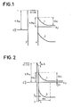
- Figure 1 shows the energy diagrams of a metal and an n-type semiconductor before contact.
- the left part of the figure relates to the metallic material, limited by its surface 3, of the future contact and the right part to the semiconductor material limited by its surface 4.
- These are conventional energy diagrams for a metal and a semiconductor of the type n near a free surface.
- Ep represents the Fermi level of the metal, q. ⁇ m the output work of an electron (q being the charge of the electron and ⁇ m the potential separating the Fermi Ep level from the vacuum level).
- E F represents the Fermi level of the semiconductor
- curve 1 is the lower limit of the conduction band
- curve 2 is the upper limit of the valence band
- Vbi is the surface potential of the semiconductor considered
- ⁇ bn its barrier height
- FIG. 2 represents the energy diagram of a contact made from a metal and a semiconductor defined above.
- the contact causes the alignment of the Fermi levels E F m and E F.
- ⁇ represents the interface potential.
- the area delimited by the surfaces 3 and 4 of thickness 6 represents the thickness of the interface layer.
- Wo is the width of the space charge region.
- FIGS. 1 and 2 The situation described above, and represented by FIGS. 1 and 2, applies in particular to the surfaces of gallium arsenide Ga As referenced (100) in crystallography and more generally to the surfaces (100) and (110) of the materials. semiconductors formed of compounds the elements of which are located in groups III and V of the periodic table of the elements.
- the potential of a surface (100) of Ga As measured by photoemission and KELVIN probe, varies strongly around 750 mV for a surface not passivated by an appropriate physicochemical treatment.
- the potential barrier heights associated with metal-semiconductor contacts can be measured by current-voltage I (V) or capacitance-voltage C (V) methods.
- the width Wo of the space charge region is related to the bias voltage V applied in reverse on the diode by the relation: where Vbi is the surface potential, q the electron charge, Nd the density of ionized impurities and ⁇ S the dielectric constant of the semiconductor material in the space charge region.
- the reverse polarized diode has, like a capacitor of thickness Wo and dielectric constant ⁇ S , a capacitance C.
- the capacitance C per unit area is:
- the barrier In the case of contacts aiuminium-gallium arsenide (AI / Ga As) or mercury-arsenide ee gallium (Hg / Ga As) the barrier is of the order of 850 mV and therefore little different from the surface potential.
- the barrier heights are relatively high, around 950 mV. These high values are explained by a rapid diffusion of gold in the gallium arsenide which creates acceptor levels in the forbidden band, near the valence band. The Fermi level is then blocked lower in the prohibited band by volume levels which gives rise to a higher barrier.
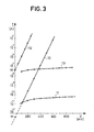
- Figure 3 is a current-voltage diagram I (V) for the diode defined in the previous paragraph.
- the axis of the currents is graduated in amperes and the axis of the voltages in millivolts.
- Curves 10 and 11 relate to a diode which has not undergone the treatment according to the invention. Curve 10 has been drawn in direct polarization and curve 11 in reverse polarization. The intersection of curve 10 with the ordinate axis (point M) gives the value of Is.
- FIG. 3 also gives the appearance of the curves I (V) in direct (curve 12) and in reverse (curve 13) for a diode having undergone a treatment according to the invention.
- This treatment consists in a preferential mode, in providing energy contributions by irradiation using a pulsed beam delivered by a laser, on semiconductor surfaces. These irradiations are carried out in an energy domain such that they do not cause fundamental degradation of the material.
- the wavelength of the laser beam pulses can be in the visible or near infrared range.
- the duration of the pulses is for example of the order of 25 nanoseconds. This allows considerable energy deposits on very small thicknesses. We can thus recrystallize semiconductor layers which have been implanted with doping impurities.
- the energetic coupling between the incident photons and the crystal lattice of the irradiated semiconductor takes place via the electronic system of the semiconductor.
- the energy absorbed by the electronic system is then transferred to the network by emission of phonons. It is assumed that for energy pulse durations of less than 500 nanoseconds, recrystallization is carried out from a liquid phase. Thicknesses of the order of a fraction of a micrometer (depending on the wavelength of the laser beam) are thus melted and the resolidification is then carried out by epitaxy on the part of the substrate which has not been melted.
- the treated diode received an energy of 480 mJ / cry 2 delivered by an irradiation having a mixture of two wavelengths: green (20%) and infrared (80%), the duration of the pulses delivered by an Nd-YAG laser being 25 ns.
- the point M ' gives the value of Is for this diode.
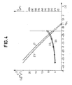
- FIG. 4 is a diagram C (V) which also gives the appearance of C -2 as a function of the voltage V applied in reverse to the diode for an untreated diode according to the invention.
- the voltage V is plotted on the abscissa.
- the axis on the right represents the values of C measured.
- the y-axis on the left represents the values of C -2 .
- Measurements of C were taken for different values of V.
- the curve 20 of the values of C was plotted for a frequency of the applied voltage of 1 MHz and transposed into a curve 21 representing C-2.
- curve 22 represents C as a function of V
- curve 23 represents C- 2 , for a frequency of 10 kHz.
- the intersections of the extensions of curves 21 and 23 with the axis of the voltages give the values of Vbi for the frequencies corresponding.
- the Vbi values noted in FIG. 4 are of the order of 0.95 V.
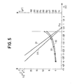
- FIG. 5 is also a diagram C (V). It is presented as in FIG. 4 but relates to a diode which has undergone the treatment according to the invention described above.
- Curves 30 and 31 respectively represent C and C -2 as a function of V, for a frequency of 1 MHz.
- Curves 32 and 33 respectively represent C and C -2 as a function of V, for a frequency of 10 kHz.
- the values of Vbi are of the order of 0.65 V, which represents a lowering of the barrier height of the order of 300 mV compared to the untreated material. The same result can of course be obtained with a ruby laser.
- the energy densities supplied must not create degradation in the volume of the irradiated material but must be high enough to initiate the melting of the surface.
- the optimal energy densities will depend on the heat capacity and the thermal conduction of the irradiated crystal as well as on the absorption length of the energy particles considered.
- gallium arsenide the energy of the irradiation doses must remain below 1.5 joule / cm 2 .
- the energy deposited must be less than 350 mJ / cm.
- the red wavelength (0.69 micrometer) it must be less than 600 mJ / cm 2 .
- the maximum admissible energy of the irradiation dose varies with the proportion of green in the green-infrared mixture.
- the lower limit of admissible energy is imposed by the effective presence of a surface fusion of the crystal and varies with the lengths of absorption.
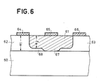
- FIG. 6 is a partial sectional view of such a transistor.
- the thickness e l makes for example, in an embodiment, 0 0 1500 A and the thickness e 2 is 1300 A.
- the zone 61 therefore has a constriction 67 of 200 A thickness.
- the electrodes 64, 65 and 66 respectively represent the source, the gate and the drain. It is admitted that for a barrier ⁇ bn gate-channel of 0.9 eV, the threshold voltage of this structure is + 0.1 V.
- a first solution consists in digging the zone 61 in order to bring the gate contact closer to the substrate 60. This structure is designated in English by the term "recess”. The major difficulty of this solution consists in adjusting the depth of the trough carried out in zone 61.
- a second solution consists in overdoping the regions of zone 61 between the source and the grid on the one hand and the grid and the drain on the other hand. This doping is carried out by self-aligned ion implantation. The difficulty of this solution lies in the need to have a stable refractory grid during the activation annealing of the implanted donor atoms (annealing temperature: approximately 800 ° C. in the case of gallium arsenide).
- the invention makes it possible, by controlling the height of the metal-semiconductor barrier, to reduce this barrier (between source and gate and between gate and drain). It is possible, in the case of an n-type semiconductor, to lower this barrier by 300 mV in the example cited above. Since the contact resistance is directly linked to doping and the barrier height, good ohmic contacts can be obtained by combining overdoping techniques and barrier height control.
- the irradiation by laser beams of the upper face of the transistor of FIG. 6 makes it possible to reduce the thickness e 2 and therefore the access resistance of the structure. By subjecting this structure to a treatment under the conditions set out above, it is possible to reduce e 2 to 1000 A and therefore increase the thickness of the access zone 68 to the conduction channel by 150%.
- the catch source and drain ohmic contacts is also improved.
- the laser radiation will only affect the surface of the semiconductor and not the electrodes. Indeed, for practical reasons of representation, the electrodes 64, 65 and 66 are not shown to scale. In fact, their thickness is of the order of a micron and their reflectivity being high (case of gold or aluminum), they are only very little affected by laser radiation.
- the treatment according to the invention makes it possible to lower the barrier height of a n-type metal-semiconductor contact, it does however raise this barrier height for a p-type metal-semiconductor contact. It is then possible to obtain Schottky diodes on p-type semiconductor with a slightly reactive metal.
- the treatment according to the invention is particularly advantageous for this type of diode since, for untreated surfaces, only the alkali metals were usable.
- the method at least partially passivates semiconductor surfaces.
Landscapes
- Electrodes Of Semiconductors (AREA)
- Junction Field-Effect Transistors (AREA)
- Formation Of Insulating Films (AREA)
Applications Claiming Priority (2)
| Application Number | Priority Date | Filing Date | Title |
|---|---|---|---|
| FR8218499 | 1982-11-04 | ||
| FR8218499A FR2535897A1 (fr) | 1982-11-04 | 1982-11-04 | Procede de passivation de la surface d'un materiau semi-conducteur et son application a la fabrication de dispositifs a semi-conducteurs |
Publications (1)
| Publication Number | Publication Date |
|---|---|
| EP0109321A1 true EP0109321A1 (fr) | 1984-05-23 |
Family
ID=9278896
Family Applications (1)
| Application Number | Title | Priority Date | Filing Date |
|---|---|---|---|
| EP83402076A Withdrawn EP0109321A1 (fr) | 1982-11-04 | 1983-10-25 | Procédé de passivation de la surface d'un matériau semi-conducteur et son application à la fabrication de dispositifs à semi-conducteur |
Country Status (3)
| Country | Link |
|---|---|
| EP (1) | EP0109321A1 (OSRAM) |
| JP (1) | JPS5998528A (OSRAM) |
| FR (1) | FR2535897A1 (OSRAM) |
Families Citing this family (2)
| Publication number | Priority date | Publication date | Assignee | Title |
|---|---|---|---|---|
| CN1154038C (zh) | 1998-04-24 | 2004-06-16 | 日本写真印刷株式会社 | 触摸面板装置 |
| CN115958302B (zh) * | 2022-12-30 | 2024-11-15 | 深圳铭创智能装备有限公司 | 一种led面板返修方法及led面板返修设备 |
-
1982
- 1982-11-04 FR FR8218499A patent/FR2535897A1/fr active Granted
-
1983
- 1983-10-25 EP EP83402076A patent/EP0109321A1/fr not_active Withdrawn
- 1983-11-04 JP JP58206096A patent/JPS5998528A/ja active Pending
Non-Patent Citations (7)
| Title |
|---|
| APPLIED PHYSICS LETTERS, vol. 34, no. 9, mai 1979, pages 558-560, American Institute of Physics, New York, US * |
| APPLIED PHYSICS LETTERS, vol. 36, no. 1, janvier 1980, pages 56-59, American Institute of Physics, New York, US * |
| EXTENDED ABSTRACTS, vol. 79-2, 14-19 octobre 1979, Fall meeting, pages 1279-1281, abrégé no. 506, Princeton, US * |
| EXTENDED ABSTRACTS, vol. 82-2, octobre 1982, pages 248-249, abrégé no. 157, Pennington, New Jersey, US * |
| IEEE ELECTRON DEVICE LETTERS, vol. EDL-2, no. 5, mai 1981, pages 115-117, IEEE, New York, US * |
| PATENTS ABSTRACTS OF JAPAN, vol. 6, no. 155 (E-125)[1033], 17 août 1982 * |
| PATENTS ABSTRACTS OF JAPAN, vol. 6, no. 9 (E-90)[887], 20 janvier 1982 * |
Also Published As
| Publication number | Publication date |
|---|---|
| FR2535897A1 (fr) | 1984-05-11 |
| JPS5998528A (ja) | 1984-06-06 |
| FR2535897B1 (OSRAM) | 1985-02-08 |
Similar Documents
| Publication | Publication Date | Title |
|---|---|---|
| Rohatgi | A study of efficiency limiting defects in polycrystalline CdTe/CdS solar cells | |
| DE2624348A1 (de) | Heterouebergang-pn-diodenphotodetektor | |
| FR2700890A1 (fr) | Dispositif à transistor composé à effet de champ ayant une électrode de Schottky. | |
| EP0092266B1 (fr) | Procédé de fabrication de transistors à effet de champ, en GaAs, par implantations ioniques et transistors ainsi obtenus | |
| US4865923A (en) | Selective intermixing of layered structures composed of thin solid films | |
| Spitzer et al. | Electrical and optical properties of proton‐bombarded gallium phosphide | |
| EP0393924B1 (en) | Devices having asymmetric delta-doping | |
| EP0109321A1 (fr) | Procédé de passivation de la surface d'un matériau semi-conducteur et son application à la fabrication de dispositifs à semi-conducteur | |
| Chow et al. | Sub-bandgap photoresponse and leakage current analysis in gold thin film-hyperdoped silicon photodiodes | |
| Tan et al. | Ion-implanted GaAs for subpicosecond optoelectronic applications | |
| US5031012A (en) | Devices having asymmetric delta-doping | |
| Dawar et al. | Effect of laser annealing on electrical and optical properties of n‐mercury cadmium telluride | |
| Lu et al. | Forward leakage currents in GaN pin diodes | |
| FR2550662A1 (fr) | Dispositif a effet de champ utilisant une condition de figeage des porteurs majoritaires | |
| Zhang et al. | Defect‐induced Schottky barrier height modification by pulsed laser melting of GaAs | |
| WO2000024054A1 (fr) | Structure comportant une couche semiconductrice et/ou des elements electroniques sur un support isolant et son procede de fabrication | |
| Asmontas et al. | Photoelectrical properties of nonuniform semiconductor under infrared laser radiation | |
| Yamada et al. | Recovery of damaged GaAs diodes by minority carrier injection | |
| Bräunlich | Light Effects on Space‐Charge Controlled Currents in CdS | |
| Zerrai et al. | Properties of the titanium related level in Cd 0.96 Zn 0.04 Te crystals | |
| Polyakov et al. | High‐resistivity GaAs grown by high‐temperature molecular‐beam epitaxy | |
| Anderson et al. | High‐speed planar GaAs photoconductors with surface implant layers | |
| JP2514169B2 (ja) | Ii−v族化合物半導体の製造方法 | |
| DE102024115314A1 (de) | Infrarot-Photodetektor und Verfahren zum Herstellen eines Infrarot-Photodetektors | |
| Gupta et al. | Ultrafast Properties and Applications of GaAs and InP Based Materials Grown by MBE at Low Temperatures |
Legal Events
| Date | Code | Title | Description |
|---|---|---|---|
| PUAI | Public reference made under article 153(3) epc to a published international application that has entered the european phase |
Free format text: ORIGINAL CODE: 0009012 |
|
| AK | Designated contracting states |
Designated state(s): DE GB IT NL |
|
| 17P | Request for examination filed |
Effective date: 19841110 |
|
| STAA | Information on the status of an ep patent application or granted ep patent |
Free format text: STATUS: THE APPLICATION IS DEEMED TO BE WITHDRAWN |
|
| 18D | Application deemed to be withdrawn |
Effective date: 19860501 |
|
| RIN1 | Information on inventor provided before grant (corrected) |
Inventor name: DIEUMEGARD, DOMINIQUE Inventor name: PRIBAT, DIDIER Inventor name: DELAGE, SYLVAIN Inventor name: POIRIER, RAYMOND |