EP0107931A2 - Selective plating - Google Patents
Selective plating Download PDFInfo
- Publication number
- EP0107931A2 EP0107931A2 EP83305977A EP83305977A EP0107931A2 EP 0107931 A2 EP0107931 A2 EP 0107931A2 EP 83305977 A EP83305977 A EP 83305977A EP 83305977 A EP83305977 A EP 83305977A EP 0107931 A2 EP0107931 A2 EP 0107931A2
- Authority
- EP
- European Patent Office
- Prior art keywords
- plating
- mask
- component
- header
- plated
- Prior art date
- Legal status (The legal status is an assumption and is not a legal conclusion. Google has not performed a legal analysis and makes no representation as to the accuracy of the status listed.)
- Granted
Links
- 238000007747 plating Methods 0.000 title claims abstract description 48
- 238000000034 method Methods 0.000 claims abstract description 23
- PCHJSUWPFVWCPO-UHFFFAOYSA-N gold Chemical compound [Au] PCHJSUWPFVWCPO-UHFFFAOYSA-N 0.000 claims abstract description 13
- 239000010931 gold Substances 0.000 claims abstract description 13
- 229910052737 gold Inorganic materials 0.000 claims abstract description 13
- 229920002379 silicone rubber Polymers 0.000 claims abstract description 6
- 239000004945 silicone rubber Substances 0.000 claims abstract description 6
- 239000000463 material Substances 0.000 claims description 3
- WABPQHHGFIMREM-UHFFFAOYSA-N lead(0) Chemical compound [Pb] WABPQHHGFIMREM-UHFFFAOYSA-N 0.000 abstract 1
- 239000002184 metal Substances 0.000 description 4
- 229910052751 metal Inorganic materials 0.000 description 4
- 229910000831 Steel Inorganic materials 0.000 description 3
- 239000010959 steel Substances 0.000 description 3
- PXHVJJICTQNCMI-UHFFFAOYSA-N Nickel Chemical compound [Ni] PXHVJJICTQNCMI-UHFFFAOYSA-N 0.000 description 2
- 239000000956 alloy Substances 0.000 description 2
- 229910045601 alloy Inorganic materials 0.000 description 2
- 239000003792 electrolyte Substances 0.000 description 2
- 239000011521 glass Substances 0.000 description 2
- 238000007654 immersion Methods 0.000 description 2
- 150000002739 metals Chemical class 0.000 description 2
- 239000000523 sample Substances 0.000 description 2
- 229910001369 Brass Inorganic materials 0.000 description 1
- 239000010951 brass Substances 0.000 description 1
- 239000004020 conductor Substances 0.000 description 1
- 238000002788 crimping Methods 0.000 description 1
- 230000000694 effects Effects 0.000 description 1
- 229920001971 elastomer Polymers 0.000 description 1
- 238000003780 insertion Methods 0.000 description 1
- 230000037431 insertion Effects 0.000 description 1
- 230000000873 masking effect Effects 0.000 description 1
- 229910052759 nickel Inorganic materials 0.000 description 1
- 239000004033 plastic Substances 0.000 description 1
- 229920003023 plastic Polymers 0.000 description 1
- 230000009467 reduction Effects 0.000 description 1
- 239000004065 semiconductor Substances 0.000 description 1
Images


Classifications
-
- H—ELECTRICITY
- H01—ELECTRIC ELEMENTS
- H01L—SEMICONDUCTOR DEVICES NOT COVERED BY CLASS H10
- H01L21/00—Processes or apparatus adapted for the manufacture or treatment of semiconductor or solid state devices or of parts thereof
- H01L21/02—Manufacture or treatment of semiconductor devices or of parts thereof
- H01L21/04—Manufacture or treatment of semiconductor devices or of parts thereof the devices having potential barriers, e.g. a PN junction, depletion layer or carrier concentration layer
- H01L21/48—Manufacture or treatment of parts, e.g. containers, prior to assembly of the devices, using processes not provided for in a single one of the subgroups H01L21/06 - H01L21/326
- H01L21/4814—Conductive parts
- H01L21/4871—Bases, plates or heatsinks
-
- C—CHEMISTRY; METALLURGY
- C25—ELECTROLYTIC OR ELECTROPHORETIC PROCESSES; APPARATUS THEREFOR
- C25D—PROCESSES FOR THE ELECTROLYTIC OR ELECTROPHORETIC PRODUCTION OF COATINGS; ELECTROFORMING; APPARATUS THEREFOR
- C25D17/00—Constructional parts, or assemblies thereof, of cells for electrolytic coating
- C25D17/004—Sealing devices
-
- C—CHEMISTRY; METALLURGY
- C25—ELECTROLYTIC OR ELECTROPHORETIC PROCESSES; APPARATUS THEREFOR
- C25D—PROCESSES FOR THE ELECTROLYTIC OR ELECTROPHORETIC PRODUCTION OF COATINGS; ELECTROFORMING; APPARATUS THEREFOR
- C25D5/00—Electroplating characterised by the process; Pretreatment or after-treatment of workpieces
- C25D5/02—Electroplating of selected surface areas
-
- H—ELECTRICITY
- H01—ELECTRIC ELEMENTS
- H01L—SEMICONDUCTOR DEVICES NOT COVERED BY CLASS H10
- H01L2924/00—Indexing scheme for arrangements or methods for connecting or disconnecting semiconductor or solid-state bodies as covered by H01L24/00
- H01L2924/0001—Technical content checked by a classifier
- H01L2924/0002—Not covered by any one of groups H01L24/00, H01L24/00 and H01L2224/00
Definitions
- THIS INVENTION relates to selective plating, in particular the selective plating with electrodepositable metals and alloys such as gold of discrete components which may otherwise be difficult to plate selectively, such as integrated circuit (lC) headers.
- electrodepositable metals and alloys such as gold of discrete components which may otherwise be difficult to plate selectively, such as integrated circuit (lC) headers.
- Certain types of component are, because of their shape, difficult to plate selectively. This is particularly applicable to components in which wires pass through a conductive member but are not conductively connected thereto, where it is required to plate the ends of the wire and the surface of the conductive member surrounding the same.
- An example of this type of component is an IC header, which comprises a base for a semiconductor device, or a transistor can, with hermetically sealed insulated leads extending through an insulating medium such as glass or a rigid plastics material
- bonding between the component and the plating medium may be poor, resulting in poor component performance, and smaller components may be damaged by barrel plating. It has been proposed to improve bonding by adding "fill" in the form of particulate steel to the plating container. However, the process of recovering gold which has been electrodeposited on the fill during plating is expensive and time consuming.
- the present invention provides a method of selective plating a component, wherein at least a part of the component is engaged in a plating aperture of a mask by resilient deformation of the mask so as to expose only the area to be plated, as well as a component whenever plated using the method and a mask for use in the method.
- a "peel-off" mask is used in which the components to be plated are press-fitted and then plated in a selective plating machine.
- the mask comprises a silicone rubber having a hardness of from 12 0 to 80 0 shore, the hardness of the silicone rubber increasing with the size of the component. (A mask of this type will last for about 3 months when in continuous use for 8 hours per day). Additional masking may be applied to reduce even further the area of the component which is exposed to electrolyte.
- each component to be plated is mounted in one of a plurality of rigidly inter-connected jigs, a metal-to-metal cathode contact being provtded in each jig, for example as described and illustrated in U.K.
- Patent Specification No. 1,447,027 a mask having a plurality of plating apertures is press fited to the jigs and to the components mounted therein and the whole apparatus is inverted over a plating tank in a selective plating machine (as opposed to previously proposed arrangements in which the bottom mask is a fixture in the plating machine).
- the method of the present invention could also be used in conjunction with the contactless plating technique described and illustrated in European Patent Application No. 83301946.6.
- plating is effected in the conventional manner utilizing, for example, an appropriate one of the commercially available plating solutions.
- a suitable current density for gold plating headers in the "Carousel" type selective plating machine is about 15 amp/dm 2 (1500 amp/m 2 ) of cathode interface.
- the method of the. present invention can be used to plate with any electrodepositable metal or alloy.
- the method will be of particular utility in plating with relatively expensive metals such as gold.
- gold for example, in the case of T046 type headers, which are normally all over barrel plated, it is estimated that a cost saving in gold of the order of US$1,600 per 100,000 units could be obtained using the method of the present invention (gold at US$414 per Troy oz).
- a saving of the order of US$300 per 100,000 units could be obtained, relative to partial immersion plating.
- the present invention provides an alternative to the barrel plating process, particularly for small headers such as T046 types, with the cost advantages of selectivity.
- the present invention can also enable processing to be carried out more quickly than hitherto, resulting in further cost savings.
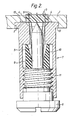
- the first mask I comprises a silicone rubber (supplied by Dow Corning) having a hardness of about 40 0 shore and is provided with a plurality of plating apertures 2.
- the header 3 comprises a cap 4 and lead wires 5 of conductive material and a glass disc 6 in which the lead wires 5 are hermetically sealed.
- the jig 7 comprises an externally threaded base 8 of machined steel, a brass probe 9 fixedly mounted thereon, an inner rubber sleeve 10 having a tapered bore for holding the lead wires 5 in electrical contact with the probe 9 and an internally screw threaded outer sleeve 1 of machined steel which surrounds the lead wires 5.
- the outer sleeve 1 is chamfered to guide insertion of the lead wires 5 into the assembled jig 7 and is provided with a beading 12.
- Each of the plating apertures 2 in the mask I is stepped so that the same can be fitted onto the cap 4 of a header 3 and the beading 12 of the associated jig 7, the cap 4 then being just proud of the mask surface.
- headers 3 are first barrel plated with nickel, then loaded manually or automatically into jigs 7 which are rigidly interconnected in groups corresponding to the number of plating apertures 2 in a mask I by means of plate members (not shown).
- a mask I is then press fitted to each group of jigs 7 and to the headers 3 mounted therein so as to expose only the end face of the cap 4 and the ends of the lead wires 5 of each header 3.
- the whole assembly is then inverted over a plating tank in a selective plating machine, clamped in position either pneumatically, hydraulically or mechanically and selective plating is carried out.
- the mask I is peeled away from the header 3 after plating.
- a chip is soldered to the end face of the cap 4 and connected electrically to one or more of the ends of the lead wires 5.
- a part, for example half, of the end face of the cap 4 is plated with gold. This can be effected using a further mask having D-shaped plating apertures which is applied after the first mask I.
- the headers 3 are orientated during loading by means of tabs 13.
- the second mask 14 comprises a silicone rubber (supplied by Dow Corning) having a hardness of about 70° shore and is provided with a plurality of plating apertures 15.
- Figures 4 and 5 illustrate the use of the second mask 14 for selective plating military-type sockets 16, such that selective plating is achieved on the inner surface (where it is required) and not on the outer surface.
- the plating apertures 15 are slotted in the same manner as the sockets, thus allowing electrolyte to flow over the inner surface to be selectively plated.
Landscapes
- Chemical & Material Sciences (AREA)
- Engineering & Computer Science (AREA)
- Metallurgy (AREA)
- Chemical Kinetics & Catalysis (AREA)
- Organic Chemistry (AREA)
- Materials Engineering (AREA)
- Electrochemistry (AREA)
- Microelectronics & Electronic Packaging (AREA)
- Condensed Matter Physics & Semiconductors (AREA)
- Power Engineering (AREA)
- General Physics & Mathematics (AREA)
- Computer Hardware Design (AREA)
- Physics & Mathematics (AREA)
- Manufacturing & Machinery (AREA)
- Electroplating Methods And Accessories (AREA)
- Glass Compositions (AREA)
- Lead Frames For Integrated Circuits (AREA)
Abstract
Description
- THIS INVENTION relates to selective plating, in particular the selective plating with electrodepositable metals and alloys such as gold of discrete components which may otherwise be difficult to plate selectively, such as integrated circuit (lC) headers.
- Certain types of component are, because of their shape, difficult to plate selectively. This is particularly applicable to components in which wires pass through a conductive member but are not conductively connected thereto, where it is required to plate the ends of the wire and the surface of the conductive member surrounding the same. An example of this type of component is an IC header, which comprises a base for a semiconductor device, or a transistor can, with hermetically sealed insulated leads extending through an insulating medium such as glass or a rigid plastics material
- In the past, components of this type, in particular smaller components.such as:T046 type headers, have either had the lead wires crimped together and then the whole barrel plated (a process of plating in which the components to be plated are placed in a rotating container provided with negative contracts) or the whole have been barrel plated without even crimping the ends together. Besides it being expensive to operate such processes, the wastage in gold (when gold is the plating medium) is phenomenal since parts of the components are being plated which do not require plating. This problem is exacerbated by the fact that the lead wires tend to be plated in preference to the ends of the wire and the can. In some commercial operations, this wastage of gold is so important that after assembly of the plated component the excess gold is removed from the lead wires. Also, bonding between the component and the plating medium may be poor, resulting in poor component performance, and smaller components may be damaged by barrel plating. It has been proposed to improve bonding by adding "fill" in the form of particulate steel to the plating container. However, the process of recovering gold which has been electrodeposited on the fill during plating is expensive and time consuming.
- Similar problems arise with other components. For example, all military-type sockets (and pins) are normally barrel plated (all over coverage), or selectively plated by partial immersion (inside and out). In the latter case, the outer surface receives a plating thickness of the order of twice that on the inner surface, where it is actually required.
- It is an object of the present invention to enable the provision of a method of selective plating a component whereby the above disadvantages may be overcome, or at least mitigated.
- Accordingly, the present invention provides a method of selective plating a component, wherein at least a part of the component is engaged in a plating aperture of a mask by resilient deformation of the mask so as to expose only the area to be plated, as well as a component whenever plated using the method and a mask for use in the method. Preferably, a "peel-off" mask is used in which the components to be plated are press-fitted and then plated in a selective plating machine. Advantageously, the mask comprises a silicone rubber having a hardness of from 120 to 800 shore, the hardness of the silicone rubber increasing with the size of the component. (A mask of this type will last for about 3 months when in continuous use for 8 hours per day). Additional masking may be applied to reduce even further the area of the component which is exposed to electrolyte.
- The method of the present invention may be used in any suitable selective plating machine, such as the "Cresta" type machine of S.G. Owen Limited, which is in commercial use in the United Kingdom, or the "Carousel" type machine of S.G. Owen Limited, which is in commercial use in the United Kingdom and the United States of America. In all cases where Carousel, Cresta or similar machines are used the time saved by the use of the "peel-off" masks could give significant reductions in labour costs. Advantageously, each component to be plated is mounted in one of a plurality of rigidly inter-connected jigs, a metal-to-metal cathode contact being provtded in each jig, for example as described and illustrated in U.K. Patent Specification No. 1,447,027, a mask having a plurality of plating apertures is press fited to the jigs and to the components mounted therein and the whole apparatus is inverted over a plating tank in a selective plating machine (as opposed to previously proposed arrangements in which the bottom mask is a fixture in the plating machine). However, the method of the present invention could also be used in conjunction with the contactless plating technique described and illustrated in European Patent Application No. 83301946.6. Apart from the use of the "peel-off" mask of the present invention, plating is effected in the conventional manner utilizing, for example, an appropriate one of the commercially available plating solutions. A suitable current density for gold plating headers in the "Carousel" type selective plating machine is about 15 amp/dm2 (1500 amp/m2) of cathode interface.
- The method of the. present invention can be used to plate with any electrodepositable metal or alloy. However, it is envisaged that the method will be of particular utility in plating with relatively expensive metals such as gold. For example, in the case of T046 type headers, which are normally all over barrel plated, it is estimated that a cost saving in gold of the order of US$1,600 per 100,000 units could be obtained using the method of the present invention (gold at US$414 per Troy oz). In the case of military-type sockets, a saving of the order of US$300 per 100,000 units could be obtained, relative to partial immersion plating.
- Thus, the present invention provides an alternative to the barrel plating process, particularly for small headers such as T046 types, with the cost advantages of selectivity. The present invention can also enable processing to be carried out more quickly than hitherto, resulting in further cost savings.
- For a better understanding of the present invention, and to show how the same may be put into effect, reference will now be made, by way of example, to the accompanying drawings, in which:
- FIGURE I is a perspective view of a first mask in accordance with the invention,
- FIGURE 2 is a vertical sectional view of a jig holding a header and having the mask of Figure I press fitted thereto,
- FIGURE 3 is a perspective view of a second mask in accordance with the invention,
- Figure 4 is a vertical sectional view of military-type sockets press fitted into the mask of Figure 3, and
- FIGURE 5 is a view on arrow V in Figure 4.
- Referring now to Figures I and 2 of the drawings, the first mask I comprises a silicone rubber (supplied by Dow Corning) having a hardness of about 400 shore and is provided with a plurality of
plating apertures 2. The header 3 comprises a cap 4 andlead wires 5 of conductive material and aglass disc 6 in which thelead wires 5 are hermetically sealed. Thejig 7 comprises an externally threadedbase 8 of machined steel, a brass probe 9 fixedly mounted thereon, aninner rubber sleeve 10 having a tapered bore for holding thelead wires 5 in electrical contact with the probe 9 and an internally screw threaded outer sleeve 1 of machined steel which surrounds thelead wires 5. The outer sleeve 1 is chamfered to guide insertion of thelead wires 5 into the assembledjig 7 and is provided with a beading 12. Each of theplating apertures 2 in the mask I is stepped so that the same can be fitted onto the cap 4 of a header 3 and the beading 12 of the associatedjig 7, the cap 4 then being just proud of the mask surface. In use, headers 3 are first barrel plated with nickel, then loaded manually or automatically intojigs 7 which are rigidly interconnected in groups corresponding to the number ofplating apertures 2 in a mask I by means of plate members (not shown). A mask I is then press fitted to each group ofjigs 7 and to the headers 3 mounted therein so as to expose only the end face of the cap 4 and the ends of thelead wires 5 of each header 3. The whole assembly is then inverted over a plating tank in a selective plating machine, clamped in position either pneumatically, hydraulically or mechanically and selective plating is carried out. The mask I is peeled away from the header 3 after plating. - in normal use of a header 3, a chip is soldered to the end face of the cap 4 and connected electrically to one or more of the ends of the
lead wires 5. Thus, it is only necessary for a part, for example half, of the end face of the cap 4 to be plated with gold. This can be effected using a further mask having D-shaped plating apertures which is applied after the first mask I. In order to ensure that the correct part of the end face of the cap 4 of each header 3 is plated, the headers 3 are orientated during loading by means oftabs 13. - Referring now to Figures 3 to 5 inclusive, the
second mask 14 comprises a silicone rubber (supplied by Dow Corning) having a hardness of about 70° shore and is provided with a plurality ofplating apertures 15. Figures 4 and 5 illustrate the use of thesecond mask 14 for selective plating military-type sockets 16, such that selective plating is achieved on the inner surface (where it is required) and not on the outer surface. Theplating apertures 15 are slotted in the same manner as the sockets, thus allowing electrolyte to flow over the inner surface to be selectively plated. - The features disclosed in the foregoing description, in the followig claims and/or in the accompanying drawings may, both separately and in any combination thereof, be material for realising the invention in diverse forms thereof.
Claims (8)
- I. A method of selective plating a component, wherein at least part of the component is engaged in a plating aperture of a mask by resilient deformation of the mask so as to expose only the area to be plated.
- 2. A method according to claim 1, wherein the mask comprises a silicone rubber.
- 3. A method according to claim I or 2, wherein the mask comprises a material having a hardness of from 120 to 80° shore.
- 4. - A method according to any one of the preceding claims, wherein the plating aperture comprises first and second portions of respective different cross sectional areas.
- 5. A method according to claim 4, wherein a part of the component is engaged in the first portion, and a part of a support means for the component is engaged in the second portion, of the plating aperture.
- 6. A method according to any one of the preceding claims, wherein the component comprises an IC header.
- 7. A method according to any one of claims 1 to 5, wherein the component comprises a military-type socket.
- 8. A method according to any one of the preceding claims, wherein the component is selectively plated with gold.
Priority Applications (1)
| Application Number | Priority Date | Filing Date | Title |
|---|---|---|---|
| AT83305977T ATE40157T1 (en) | 1982-10-05 | 1983-09-30 | SELECTIVE PLATING. |
Applications Claiming Priority (2)
| Application Number | Priority Date | Filing Date | Title |
|---|---|---|---|
| GB8228376 | 1982-10-05 | ||
| GB8228376 | 1982-10-05 |
Publications (3)
| Publication Number | Publication Date |
|---|---|
| EP0107931A2 true EP0107931A2 (en) | 1984-05-09 |
| EP0107931A3 EP0107931A3 (en) | 1984-08-08 |
| EP0107931B1 EP0107931B1 (en) | 1989-01-18 |
Family
ID=10533382
Family Applications (1)
| Application Number | Title | Priority Date | Filing Date |
|---|---|---|---|
| EP83305977A Expired EP0107931B1 (en) | 1982-10-05 | 1983-09-30 | Selective plating |
Country Status (5)
| Country | Link |
|---|---|
| EP (1) | EP0107931B1 (en) |
| JP (1) | JPS5985886A (en) |
| AT (1) | ATE40157T1 (en) |
| DE (1) | DE3378982D1 (en) |
| GB (1) | GB2127855B (en) |
Cited By (1)
| Publication number | Priority date | Publication date | Assignee | Title |
|---|---|---|---|---|
| US20080302300A1 (en) * | 2007-06-05 | 2008-12-11 | Lee Jung Gul | Jig for surface-treatment of thread portion of nut |
Families Citing this family (10)
| Publication number | Priority date | Publication date | Assignee | Title |
|---|---|---|---|---|
| GB2152854A (en) * | 1983-12-27 | 1985-08-14 | Champion Spark Plug Co | Coating portions of articles |
| US4561954A (en) * | 1985-01-22 | 1985-12-31 | Avx Corporation | Method of applying terminations to ceramic bodies |
| JPS62191871U (en) * | 1986-05-27 | 1987-12-05 | ||
| JPH0680605B2 (en) * | 1987-11-28 | 1994-10-12 | 株式会社村田製作所 | Electronic component chip holding jig and metal coating method for metallized surface of electronic component chip |
| GB2270527A (en) * | 1992-09-11 | 1994-03-16 | Rolls Royce Plc | Coating a face of a component using apertured mask of same size as the face; turbine tip blades |
| GB9326082D0 (en) * | 1993-12-21 | 1994-02-23 | Baj Coatings Ltd | Rotor blades |
| CA2572499A1 (en) * | 1997-04-04 | 1998-10-15 | University Of Southern California | Method for electrochemical fabrication including use of multiple structural and/or sacrificial materials |
| WO2003049514A2 (en) | 2001-12-03 | 2003-06-12 | Memgen Corporation | Miniature rf and microwave components and methods for fabricating such components |
| US9614266B2 (en) | 2001-12-03 | 2017-04-04 | Microfabrica Inc. | Miniature RF and microwave components and methods for fabricating such components |
| US10297421B1 (en) | 2003-05-07 | 2019-05-21 | Microfabrica Inc. | Plasma etching of dielectric sacrificial material from reentrant multi-layer metal structures |
Citations (4)
| Publication number | Priority date | Publication date | Assignee | Title |
|---|---|---|---|---|
| US3257308A (en) * | 1961-07-11 | 1966-06-21 | Western Electric Co | Article holder for electroplating articles |
| US3658663A (en) * | 1970-03-03 | 1972-04-25 | Japan Electro Plating Co | Method for effecting partial metal plating |
| GB1447027A (en) * | 1972-05-25 | 1976-08-25 | Owen S G Ltd | Plating |
| EP0055130A1 (en) * | 1980-12-23 | 1982-06-30 | S.G. Owen Limited | Improvements in or relating to selective plating |
Family Cites Families (9)
| Publication number | Priority date | Publication date | Assignee | Title |
|---|---|---|---|---|
| US3835017A (en) * | 1972-12-22 | 1974-09-10 | Buckbee Mears Co | Reusable shields for selective electrodeposition |
| US3897323A (en) * | 1974-08-05 | 1975-07-29 | Motorola Inc | Apparatus for selective plating |
| JPS52915U (en) * | 1975-06-21 | 1977-01-06 | ||
| GB1544951A (en) * | 1976-03-23 | 1979-04-25 | Electroplating Engs Of Ja Ltd | Device for plating a selected portion of opposite side surfaces of a sheet-like article |
| GB1549862A (en) * | 1976-04-20 | 1979-08-08 | Owens Ltd S | Electroplating |
| GB2067597B (en) * | 1980-01-17 | 1982-11-17 | Owen S G Ltd | Plating |
| GB2088411B (en) * | 1980-12-02 | 1983-11-30 | Ferranti Ltd | Positioning electrical contacts for electroplating |
| GB2094344B (en) * | 1980-12-23 | 1983-09-07 | Owen S G Ltd | Improvements in or relating to selective plating |
| US4405410A (en) * | 1982-01-15 | 1983-09-20 | Northern Telecom Limited | Masking of elongate three dimensional objects for the exposure of preselected areas for surface treatment |
-
1983
- 1983-09-30 AT AT83305977T patent/ATE40157T1/en not_active IP Right Cessation
- 1983-09-30 EP EP83305977A patent/EP0107931B1/en not_active Expired
- 1983-09-30 DE DE8383305977T patent/DE3378982D1/en not_active Expired
- 1983-09-30 GB GB08326303A patent/GB2127855B/en not_active Expired
- 1983-10-05 JP JP58186676A patent/JPS5985886A/en active Granted
Patent Citations (4)
| Publication number | Priority date | Publication date | Assignee | Title |
|---|---|---|---|---|
| US3257308A (en) * | 1961-07-11 | 1966-06-21 | Western Electric Co | Article holder for electroplating articles |
| US3658663A (en) * | 1970-03-03 | 1972-04-25 | Japan Electro Plating Co | Method for effecting partial metal plating |
| GB1447027A (en) * | 1972-05-25 | 1976-08-25 | Owen S G Ltd | Plating |
| EP0055130A1 (en) * | 1980-12-23 | 1982-06-30 | S.G. Owen Limited | Improvements in or relating to selective plating |
Cited By (1)
| Publication number | Priority date | Publication date | Assignee | Title |
|---|---|---|---|---|
| US20080302300A1 (en) * | 2007-06-05 | 2008-12-11 | Lee Jung Gul | Jig for surface-treatment of thread portion of nut |
Also Published As
| Publication number | Publication date |
|---|---|
| ATE40157T1 (en) | 1989-02-15 |
| GB2127855A (en) | 1984-04-18 |
| GB8326303D0 (en) | 1983-11-02 |
| JPS5985886A (en) | 1984-05-17 |
| EP0107931B1 (en) | 1989-01-18 |
| DE3378982D1 (en) | 1989-02-23 |
| GB2127855B (en) | 1986-03-26 |
| EP0107931A3 (en) | 1984-08-08 |
| JPH0411633B2 (en) | 1992-03-02 |
Similar Documents
| Publication | Publication Date | Title |
|---|---|---|
| US6071388A (en) | Electroplating workpiece fixture having liquid gap spacer | |
| EP0107931B1 (en) | Selective plating | |
| EP0155080A2 (en) | Contact for chip carrier and method of inserting same into a housing | |
| US20020001872A1 (en) | Semiconductor package having semiconductor element mounting structure of semiconductor package mounted on circuit board and method of assembling semiconductor package | |
| US5223110A (en) | Apparatus for electroplating electrical contacts | |
| US4780098A (en) | Conductive lead arrangement | |
| US5580432A (en) | Jig for electroplating lead pins of an integrated circuit package | |
| US4395087A (en) | Strip of border-held contact elements for a connection device, and a process for forming such contact elements | |
| US6181057B1 (en) | Electrode assembly, cathode device and plating apparatus including an insulating member covering an internal circumferential edge of a cathode member | |
| US6203690B1 (en) | Process of reworking pin grid array chip carriers | |
| US6527935B2 (en) | Process for electroplating pins of an integrated circuit package | |
| US6497805B2 (en) | Method for shorting pin grid array pins for plating | |
| EP0101539A2 (en) | Printed circuit board finger connector and method of manufacture | |
| EP0640701A1 (en) | A partial plating method for a plate member and masking jig for use therein | |
| JPH0813198A (en) | Electrode for contact conduction and apparatus for producing semiconductor using the same | |
| US20020177342A1 (en) | Contact pin and socket for electrical parts | |
| US6184613B1 (en) | Electrode assembly, cathode device and plating apparatus including a gap configured to eliminate a concentration of a line of electrical force at a boundary between a cathode and plate forming surface of an object | |
| US20030153201A1 (en) | Circuit board electrical lead frame | |
| JP3000084B2 (en) | Conducting jig for plating and method of manufacturing wiring board using the same | |
| JP3167782B2 (en) | High-speed solder plating equipment for electronic components | |
| JPH07207497A (en) | Method for plating electronic parts and plating jig | |
| JPH06302720A (en) | Manufacture of package for integrated circuit | |
| JPH0823063A (en) | Ic package plating frame and dismounting method thereof | |
| JPH06302742A (en) | Jig for plating | |
| JPH08316269A (en) | Semiconductor chip, chip holder and manufacture of semiconductor device used therefor |
Legal Events
| Date | Code | Title | Description |
|---|---|---|---|
| PUAI | Public reference made under article 153(3) epc to a published international application that has entered the european phase |
Free format text: ORIGINAL CODE: 0009012 |
|
| AK | Designated contracting states |
Designated state(s): AT BE CH DE FR GB IT LI LU NL SE |
|
| PUAL | Search report despatched |
Free format text: ORIGINAL CODE: 0009013 |
|
| AK | Designated contracting states |
Designated state(s): AT BE CH DE FR GB IT LI LU NL SE |
|
| 17P | Request for examination filed |
Effective date: 19841015 |
|
| RAP1 | Party data changed (applicant data changed or rights of an application transferred) |
Owner name: S.G. OWEN (NORTHAMPTON) LIMITED |
|
| GRAA | (expected) grant |
Free format text: ORIGINAL CODE: 0009210 |
|
| AK | Designated contracting states |
Kind code of ref document: B1 Designated state(s): AT BE CH DE FR GB IT LI LU NL SE |
|
| REF | Corresponds to: |
Ref document number: 40157 Country of ref document: AT Date of ref document: 19890215 Kind code of ref document: T |
|
| REF | Corresponds to: |
Ref document number: 3378982 Country of ref document: DE Date of ref document: 19890223 |
|
| ET | Fr: translation filed | ||
| ITF | It: translation for a ep patent filed | ||
| PLBE | No opposition filed within time limit |
Free format text: ORIGINAL CODE: 0009261 |
|
| STAA | Information on the status of an ep patent application or granted ep patent |
Free format text: STATUS: NO OPPOSITION FILED WITHIN TIME LIMIT |
|
| 26N | No opposition filed | ||
| PGFP | Annual fee paid to national office [announced via postgrant information from national office to epo] |
Ref country code: NL Payment date: 19900930 Year of fee payment: 8 |
|
| PGFP | Annual fee paid to national office [announced via postgrant information from national office to epo] |
Ref country code: GB Payment date: 19910328 Year of fee payment: 8 Ref country code: CH Payment date: 19910328 Year of fee payment: 8 |
|
| PGFP | Annual fee paid to national office [announced via postgrant information from national office to epo] |
Ref country code: LU Payment date: 19910329 Year of fee payment: 8 Ref country code: FR Payment date: 19910329 Year of fee payment: 8 Ref country code: BE Payment date: 19910329 Year of fee payment: 8 |
|
| BERE | Be: lapsed |
Owner name: S.G. OWEN (NORTHAMPTON) LTD Effective date: 19900930 |
|
| PGFP | Annual fee paid to national office [announced via postgrant information from national office to epo] |
Ref country code: AT Payment date: 19910331 Year of fee payment: 8 |
|
| PGFP | Annual fee paid to national office [announced via postgrant information from national office to epo] |
Ref country code: SE Payment date: 19910402 Year of fee payment: 8 Ref country code: DE Payment date: 19910402 Year of fee payment: 8 |
|
| EPTA | Lu: last paid annual fee | ||
| ITTA | It: last paid annual fee | ||
| PG25 | Lapsed in a contracting state [announced via postgrant information from national office to epo] |
Ref country code: LU Free format text: LAPSE BECAUSE OF NON-PAYMENT OF DUE FEES Effective date: 19910930 Ref country code: LI Effective date: 19910930 Ref country code: GB Effective date: 19910930 Ref country code: CH Effective date: 19910930 Ref country code: BE Effective date: 19910930 Ref country code: AT Effective date: 19910930 |
|
| PG25 | Lapsed in a contracting state [announced via postgrant information from national office to epo] |
Ref country code: SE Effective date: 19911001 |
|
| BERE | Be: lapsed |
Owner name: S.G. OWEN (NORTHAMPTON) LTD Effective date: 19910930 |
|
| PG25 | Lapsed in a contracting state [announced via postgrant information from national office to epo] |
Ref country code: NL Effective date: 19920401 |
|
| NLV4 | Nl: lapsed or anulled due to non-payment of the annual fee | ||
| GBPC | Gb: european patent ceased through non-payment of renewal fee | ||
| PG25 | Lapsed in a contracting state [announced via postgrant information from national office to epo] |
Ref country code: FR Effective date: 19920529 |
|
| REG | Reference to a national code |
Ref country code: CH Ref legal event code: PL |
|
| PG25 | Lapsed in a contracting state [announced via postgrant information from national office to epo] |
Ref country code: DE Effective date: 19920602 |
|
| REG | Reference to a national code |
Ref country code: FR Ref legal event code: ST |
|
| EUG | Se: european patent has lapsed |
Ref document number: 83305977.7 Effective date: 19920510 |