EP0106044B1 - Raumladungsmodulierende Halbleiteranordnung und ein solche Anordnung enthaltender Schaltkreis - Google Patents
Raumladungsmodulierende Halbleiteranordnung und ein solche Anordnung enthaltender Schaltkreis Download PDFInfo
- Publication number
- EP0106044B1 EP0106044B1 EP83107607A EP83107607A EP0106044B1 EP 0106044 B1 EP0106044 B1 EP 0106044B1 EP 83107607 A EP83107607 A EP 83107607A EP 83107607 A EP83107607 A EP 83107607A EP 0106044 B1 EP0106044 B1 EP 0106044B1
- Authority
- EP
- European Patent Office
- Prior art keywords
- contact
- contacts
- semiconductor device
- semiconductor
- disposed
- Prior art date
- Legal status (The legal status is an assumption and is not a legal conclusion. Google has not performed a legal analysis and makes no representation as to the accuracy of the status listed.)
- Expired
Links
- 239000004065 semiconductor Substances 0.000 title claims description 43
- 230000004888 barrier function Effects 0.000 claims description 13
- XUIMIQQOPSSXEZ-UHFFFAOYSA-N Silicon Chemical compound [Si] XUIMIQQOPSSXEZ-UHFFFAOYSA-N 0.000 claims description 6
- 229910052710 silicon Inorganic materials 0.000 claims description 6
- 239000010703 silicon Substances 0.000 claims description 6
- 239000012535 impurity Substances 0.000 claims description 2
- 238000009825 accumulation Methods 0.000 description 2
- 239000002800 charge carrier Substances 0.000 description 2
- 238000010586 diagram Methods 0.000 description 2
- 239000000758 substrate Substances 0.000 description 2
- VLJQDHDVZJXNQL-UHFFFAOYSA-N 4-methyl-n-(oxomethylidene)benzenesulfonamide Chemical compound CC1=CC=C(S(=O)(=O)N=C=O)C=C1 VLJQDHDVZJXNQL-UHFFFAOYSA-N 0.000 description 1
- 239000000463 material Substances 0.000 description 1
- 229910021340 platinum monosilicide Inorganic materials 0.000 description 1
- 229910052761 rare earth metal Inorganic materials 0.000 description 1
- 150000002910 rare earth metals Chemical class 0.000 description 1
- 229910021332 silicide Inorganic materials 0.000 description 1
Images

Classifications
-
- H—ELECTRICITY
- H10—SEMICONDUCTOR DEVICES; ELECTRIC SOLID-STATE DEVICES NOT OTHERWISE PROVIDED FOR
- H10D—INORGANIC ELECTRIC SEMICONDUCTOR DEVICES
- H10D30/00—Field-effect transistors [FET]
- H10D30/80—FETs having rectifying junction gate electrodes
- H10D30/87—FETs having Schottky gate electrodes, e.g. metal-semiconductor FETs [MESFET]
- H10D30/871—Vertical FETs having Schottky gate electrodes
-
- H—ELECTRICITY
- H10—SEMICONDUCTOR DEVICES; ELECTRIC SOLID-STATE DEVICES NOT OTHERWISE PROVIDED FOR
- H10D—INORGANIC ELECTRIC SEMICONDUCTOR DEVICES
- H10D30/00—Field-effect transistors [FET]
- H10D30/202—FETs having static field-induced regions, e.g. static-induction transistors [SIT] or permeable base transistors [PBT]
Definitions
- This invention relates to semiconductor devices.
- the invention seeks to provide a semiconductor device in which electrical conduction between a pair of contacts is controlled by space charge modulation effected via a third contact.
- US-E-29 971 discloses (in particular in Fig. 8 thereof) a semiconductor device of the JFET type which has a body comprising two contiguous semiconductor regions of opposite conductivity type with a rectifying junction therebetween. First and second contacts are made to the two semiconductor regions. A third contact is disposed on the semiconductor body in a position remote from the first and second contacts.
- the invention provides a semiconductor device comprising first and second contacts disposed on one side of a semiconductor body, the second contact being a rectifying contact, and a third contact disposed on the semiconductor body in a position remote from the first and second contacts, the first contact having a dimension substantially equal to or less than the Debye length (as defined herein) in the semiconductor of the body, the second contact being disposed a distance substantially equal to or less than the said Debye length from the first contact, the semiconductor body being of a single conductivity type, and the second contact being shorted together with the third contact thereby providing a diode characteristic between the first contact and the third and second contacts.
- a rectifying contact is placed within a Debye length of a second contact of the order of a Debye length in size on one surface of a semiconductor body and a third contact is placed elsewhere on the same semiconductor body. Under proper biasing the space charge in the semiconductor body under the rectifying contact can control the conduction between the other two contacts.
- FIG. 1 An embodiment of a semiconductor device is represented in FIG. 1 wherein on one surface of a semiconductor body 1 there is positioned an intrinsically rectifying contact 2.
- the intrinsic conducting behaviour of a contact may be defined as the two-terminal current voltage behaviour of the contact when that contact is forming a two-terminal device with the substrate.
- the rectifying contact 2 surrounds or is parallel with a small width intrinsically ohmic contact 3 positioned a distance D from the rectifying contact 2.
- the dimension D is about equal to or less than the extrinsic Debye length of the semiconductor of body 1.
- the contact 3 has a dimension C that is also about equal to or less than the Debye length.
- a third, ohmic contact 4 is positioned a distance A from the contacts 2 and 3 on the opposite side of the semiconductor body 1.
- the semiconductor of body 1 should be of sufficiently high resistivity to permit the space charge under the rectifying contact 2 to penetrate a physical distance into the semiconductor under moderate voltage levels to affect carrier flow between the contacts 3 and 4.
- the semiconductor body 1 may be of silicon doped with 1015 impurity atoms per cubic centimeter. With this resistivity and dimensions maintained at C and D less than approximately 0.1 micrometers, the polarity of the signal on the contact 2 will affect current flow between contacts 3 and 4.
- the device of FIG. 1 is preferably fabricated by using Schottky barrier contacts with different barrier heights so that ohmic or rectifying behavior is produced.
- the semiconductor 1 is silicon doped to about 1015 atoms per cubic centimeter with conductivity type n
- the ohmic contacts 3 and 4 may be obtained using a relatively low barrier Schottky contact where that barrier height is about 0.2 to 0.3 eV.
- Such contacts can be obtained through the use of rare earth silicides as set forth in IBM Technical Disclosure Bulletin, Vol. 21, p. 2811.
- the rectifying contact 2 can be formed using a higher barrier Schottky contact.
- the barrier height should be of the order of 0.8 eV, such as is obtainable with Au or PtSi on a silicon substrate.
- FIGS. 2 through 5 An illustration of the operation of the device may be seen in connection with FIGS. 2 through 5 wherein FIGS. 2 and 3 illustrate a circuit and corresponding performance in one polarity and FIGS. 4 and 5 illustrate a circuit and corresponding performance in an opposite polarity.
- the semiconductor body 1 has one ohmic contact 4 connected to the battery 6 and the other ohmic contact 3 and rectifying contact 2 connected through a current indicator 7 to the other side of the battery 6.
- the depletion depth in 1015 atoms per cc n-type silicon radiating from contact 2 would deplete the area below contact 3 when positioned lateral to contact 2 for the intergap D of about 500 ⁇ and contact size C of 0.15 micrometers. These dimensions result in the distance from the edge of the contact 2 to the center of contact 3 being of the order of a Debye length in semiconductor material of this resistivity. This would not permit any significant current flow between contacts 3 and 4.
- the depletion depth radiating from contact 2 would decrease thus allowing a clear conducting path of electrons between contacts 3 and 4.
- That portion of the current through contact 3 dominates the flow for voltages of the order of 0.6V.
- FIG. 3 there is shown the current voltage (I-V) characteristic curve for the circuit of FIG. 2. It will be apparent to one skilled in the art that the the curve of FIG. 3 is similar to that of an ordinary I-V curve for a diode. Since the silicon of the body 1 is doped n-type in this example, the IV characteristic of contact 3 is qualitatively that of a normal Schottky diode as shown in FIG. 3.
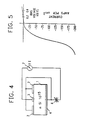
- the device of the invention it is also possible to provide an opposite or reverse diode characteristic. This is illustrated in connection with the circuit of FIG. 4 and the current voltage (IV) output characteristic of FIG. 5.
- the circuit configuration is such that the rectifying contact or contact segments 2 and the ohmic contact 4 are shorted together and the ohmic contact 3 is held at a positive potential with the battery 6.
- the (IV) characteristic of FIG. 5 is achieved by varying the voltage V of the battery 6 and observing the current flow through the current indicator 7.
- the I-V characteristic corresponding to the circuit configuration of FIG. 4 is shown in FIG. 5.
- the characteristic polarity is clearly reversed and is in marked contrast to that of FIG. 3.
- the impedance of contact 2 also remains high in this reversed diode case.
- the three-terminal device of the invention implements a reversing diode concept in that the polarity of conduction between the two contacts 3 and 4 is determined by the potential that is present on a high impedance contact 2.
Landscapes
- Electrodes Of Semiconductors (AREA)
- Junction Field-Effect Transistors (AREA)
Claims (8)
- Halbleiterbauelement mit ersten und zweiten Kontakten (3,2), die an einer Seite eines Halbleiterkörpers (1) angeordnet sind, wobei der zweite Kontakt (2) ein gleichrichtender Kontakt ist und mit einem dritten Kontakt (4), der an dem Halbleiterkörper in einer von den ersten und zweiten Kontakten entfernten Lage angeordnet ist, wobei der erste Kontakt eine Abmessung (C) aufweist, die im wesentlichen gleich oder kleiner ist, als die Debye-Länge (wie hierin definiert) in dem Halbleiter des Körpers, der zweite Kontakt in einem Abstand (D), der im wesentlichen gleich oder kleiner ist, als die Debye-Länge, von dem ersten Kontakt angeordnet ist, der Halbleiterkörper eine einzige Leitfähigkeitsart aufweist und der zweite Kontakt zusammen mit dem dritten Kontakt kurzgeschlossen ist, wodurch eine Dioden-Charakteristik zwischen dem ersten Kontakt und den dritten und zweiten Kontakten geliefert wird.
- Halbleiterbauelement nach Anspruch 1, bei welchem die ersten und dritten Kontakte (3, 4) ohmsche Kontakte sind.
- Halbleiterbauelement nach Anspruch 1 oder 2, bei welchem der dritte Kontakt (4) ein großflächiger Kontakt ist, der an der jener Seite gegenüberliegenden Seite des Körpers (1) angeordnet ist, an welcher die ersten und zweiten Kontakte (3, 2) angeordnet sind.
- Halbleiterbauelement nach irgend einem vorgehenden Anspruch, bei welchem die Abmessung (c) des ersten Kontaktes ungefähr 0,15 µm beträgt und bei welchem der zweite Kontakt ungefähr 50 nm (500 Å) von dem ersten Kontakt angeordnet ist.
- Halbleiterbauelement nach irgend einem vorgehenden Anspruch, bei welchem der erste Kontakt (3) ein Schottky-Barriere-Kontakt mit einer verhältnismäßig kleinen Barrierehöhe ist und der zweite Kontakt (2) ein Schottky-Barriere-Kontakt mit einer verhältnismäßig großen Barrierehöhe ist.
- Halbleiterbauelement nach Anspruch 5, bei welchem der erste Kontakt (3) eine Barrierehöhe von 0,2 bis 0,3 eV und der zweite Kontakt (2) eine Barrierehöhe von etwa 0,8 eV aufweist.
- Halbleiterbauelement nach irgend einem vorgehenden Anspruch, bei welchem der Halbleiterkörper (1) n-Typ Silizium ist, das mit 10¹⁵ Fremdatomen pro Kubikzentimeter dotiert ist.
- Schaltung mit einem Halbleiterbauelement nach irgend einem vorgehenden Anspruch.
Applications Claiming Priority (2)
| Application Number | Priority Date | Filing Date | Title |
|---|---|---|---|
| US419381 | 1982-09-17 | ||
| US06/419,381 US4638342A (en) | 1982-09-17 | 1982-09-17 | Space charge modulation device |
Publications (3)
| Publication Number | Publication Date |
|---|---|
| EP0106044A2 EP0106044A2 (de) | 1984-04-25 |
| EP0106044A3 EP0106044A3 (en) | 1987-03-25 |
| EP0106044B1 true EP0106044B1 (de) | 1991-07-17 |
Family
ID=23662022
Family Applications (1)
| Application Number | Title | Priority Date | Filing Date |
|---|---|---|---|
| EP83107607A Expired EP0106044B1 (de) | 1982-09-17 | 1983-08-02 | Raumladungsmodulierende Halbleiteranordnung und ein solche Anordnung enthaltender Schaltkreis |
Country Status (4)
| Country | Link |
|---|---|
| US (1) | US4638342A (de) |
| EP (1) | EP0106044B1 (de) |
| JP (1) | JPS5961190A (de) |
| DE (1) | DE3382340D1 (de) |
Families Citing this family (4)
| Publication number | Priority date | Publication date | Assignee | Title |
|---|---|---|---|---|
| JPH0687483B2 (ja) * | 1988-02-13 | 1994-11-02 | 株式会社東芝 | 半導体装置 |
| US5019530A (en) * | 1990-04-20 | 1991-05-28 | International Business Machines Corporation | Method of making metal-insulator-metal junction structures with adjustable barrier heights |
| US5612547A (en) * | 1993-10-18 | 1997-03-18 | Northrop Grumman Corporation | Silicon carbide static induction transistor |
| US9520445B2 (en) * | 2011-07-12 | 2016-12-13 | Helmholtz-Zentrum Dresden-Rossendorf E. V. | Integrated non-volatile memory elements, design and use |
Family Cites Families (12)
| Publication number | Priority date | Publication date | Assignee | Title |
|---|---|---|---|---|
| US3684902A (en) * | 1966-06-07 | 1972-08-15 | Westinghouse Electric Corp | Semiconductor switch device |
| US3549961A (en) * | 1968-06-19 | 1970-12-22 | Int Rectifier Corp | Triac structure and method of manufacture |
| USRE29971E (en) * | 1971-07-31 | 1979-04-17 | Zaidan Hojin Hondotai Kenkyn Shinkokai | Field effect semiconductor device having an unsaturated triode vacuum tube characteristic |
| JPS5039880A (de) * | 1973-08-13 | 1975-04-12 | ||
| US4066483A (en) * | 1976-07-07 | 1978-01-03 | Western Electric Company, Inc. | Gate-controlled bidirectional switching device |
| JPS5357769A (en) * | 1976-11-04 | 1978-05-25 | Mitsubishi Electric Corp | Electrostatic induction transistor |
| US4132996A (en) * | 1976-11-08 | 1979-01-02 | General Electric Company | Electric field-controlled semiconductor device |
| US4141021A (en) * | 1977-02-14 | 1979-02-20 | Varian Associates, Inc. | Field effect transistor having source and gate electrodes on opposite faces of active layer |
| US4236166A (en) * | 1979-07-05 | 1980-11-25 | Bell Telephone Laboratories, Incorporated | Vertical field effect transistor |
| JPS5636154A (en) * | 1979-09-03 | 1981-04-09 | Seiko Instr & Electronics Ltd | Mes type integrated circuit |
| DE3040873C2 (de) * | 1980-10-30 | 1984-02-23 | Licentia Patent-Verwaltungs-Gmbh, 6000 Frankfurt | Feldeffekttransistor |
| JPS56138957A (en) * | 1981-03-07 | 1981-10-29 | Semiconductor Res Found | Electrostatic induction type semiconductor device |
-
1982
- 1982-09-17 US US06/419,381 patent/US4638342A/en not_active Expired - Fee Related
-
1983
- 1983-05-31 JP JP58095124A patent/JPS5961190A/ja active Granted
- 1983-08-02 EP EP83107607A patent/EP0106044B1/de not_active Expired
- 1983-08-02 DE DE8383107607T patent/DE3382340D1/de not_active Expired - Lifetime
Also Published As
| Publication number | Publication date |
|---|---|
| DE3382340D1 (de) | 1991-08-22 |
| JPH0213928B2 (de) | 1990-04-05 |
| US4638342A (en) | 1987-01-20 |
| EP0106044A3 (en) | 1987-03-25 |
| EP0106044A2 (de) | 1984-04-25 |
| JPS5961190A (ja) | 1984-04-07 |
Similar Documents
| Publication | Publication Date | Title |
|---|---|---|
| EP0134456B1 (de) | Pinch-Effekt-Gleichrichter | |
| US5536953A (en) | Wide bandgap semiconductor device including lightly doped active region | |
| US4835581A (en) | Electron gas hole gas tunneling transistor device | |
| EP0184827A2 (de) | Hochleistungstransistor hoher Geschwindigkeit | |
| GB883906A (en) | Improvements in semi-conductive arrangements | |
| US4309714A (en) | Gate turn-off diodes and arrangements including such diodes | |
| GB805207A (en) | Electric circuit devices utilizing semiconductor bodies and circuits including such devices | |
| US4903092A (en) | Real space electron transfer device using hot electron injection | |
| US3495141A (en) | Controllable schottky diode | |
| EP0106044B1 (de) | Raumladungsmodulierende Halbleiteranordnung und ein solche Anordnung enthaltender Schaltkreis | |
| US3087099A (en) | Narrow web mesa transistor structure | |
| US3585412A (en) | Schottky barrier diodes as impedance elements | |
| US4449140A (en) | Semi-conductor barrier switching devices | |
| EP0200422B1 (de) | Transistoranordnung | |
| US4910562A (en) | Field induced base transistor | |
| EP0029717A1 (de) | Statische bipolare Speicherzelle | |
| Kroemer | Generalized proof of Shockley's positive conductance theorem | |
| EP0091710B1 (de) | Transistoren | |
| EP0064614B1 (de) | Emitterstruktur für Halbleiteranordnungen | |
| US5936284A (en) | Electrostatic discharge protection circuit and transistor | |
| Sinha et al. | Effect of heavy doping on the properties of high-low junction | |
| US4689648A (en) | Magnetically sensitive metal semiconductor devices | |
| EP0698925A2 (de) | Bipolartransistor mit schwebender Basis | |
| US3568011A (en) | Semiconductor device including a metal layer overlying the junction area | |
| Irvin et al. | Nonohmic contacts for microwave devices |
Legal Events
| Date | Code | Title | Description |
|---|---|---|---|
| PUAI | Public reference made under article 153(3) epc to a published international application that has entered the european phase |
Free format text: ORIGINAL CODE: 0009012 |
|
| AK | Designated contracting states |
Designated state(s): DE FR GB |
|
| 17P | Request for examination filed |
Effective date: 19840724 |
|
| PUAL | Search report despatched |
Free format text: ORIGINAL CODE: 0009013 |
|
| RHK1 | Main classification (correction) |
Ipc: H01L 29/80 |
|
| AK | Designated contracting states |
Kind code of ref document: A3 Designated state(s): DE FR GB |
|
| 17Q | First examination report despatched |
Effective date: 19890418 |
|
| GRAA | (expected) grant |
Free format text: ORIGINAL CODE: 0009210 |
|
| AK | Designated contracting states |
Kind code of ref document: B1 Designated state(s): DE FR GB |
|
| ET | Fr: translation filed | ||
| REF | Corresponds to: |
Ref document number: 3382340 Country of ref document: DE Date of ref document: 19910822 |
|
| PLBE | No opposition filed within time limit |
Free format text: ORIGINAL CODE: 0009261 |
|
| STAA | Information on the status of an ep patent application or granted ep patent |
Free format text: STATUS: NO OPPOSITION FILED WITHIN TIME LIMIT |
|
| 26N | No opposition filed | ||
| PGFP | Annual fee paid to national office [announced via postgrant information from national office to epo] |
Ref country code: GB Payment date: 19930720 Year of fee payment: 11 |
|
| PGFP | Annual fee paid to national office [announced via postgrant information from national office to epo] |
Ref country code: DE Payment date: 19930824 Year of fee payment: 11 |
|
| PGFP | Annual fee paid to national office [announced via postgrant information from national office to epo] |
Ref country code: FR Payment date: 19940725 Year of fee payment: 12 |
|
| PG25 | Lapsed in a contracting state [announced via postgrant information from national office to epo] |
Ref country code: GB Effective date: 19940802 |
|
| GBPC | Gb: european patent ceased through non-payment of renewal fee |
Effective date: 19940802 |
|
| PG25 | Lapsed in a contracting state [announced via postgrant information from national office to epo] |
Ref country code: DE Effective date: 19950503 |
|
| PG25 | Lapsed in a contracting state [announced via postgrant information from national office to epo] |
Ref country code: FR Effective date: 19960430 |
|
| REG | Reference to a national code |
Ref country code: FR Ref legal event code: ST |