EP0104449A2 - QAM-Demodulator der eine Kombination eines Vollweggleichrichters und binärer Detektoren enthält - Google Patents
QAM-Demodulator der eine Kombination eines Vollweggleichrichters und binärer Detektoren enthält Download PDFInfo
- Publication number
- EP0104449A2 EP0104449A2 EP83108388A EP83108388A EP0104449A2 EP 0104449 A2 EP0104449 A2 EP 0104449A2 EP 83108388 A EP83108388 A EP 83108388A EP 83108388 A EP83108388 A EP 83108388A EP 0104449 A2 EP0104449 A2 EP 0104449A2
- Authority
- EP
- European Patent Office
- Prior art keywords
- signal
- level
- rectified
- preselected
- binary
- Prior art date
- Legal status (The legal status is an assumption and is not a legal conclusion. Google has not performed a legal analysis and makes no representation as to the accuracy of the status listed.)
- Granted
Links
Images

Classifications
-
- H—ELECTRICITY
- H04—ELECTRIC COMMUNICATION TECHNIQUE
- H04L—TRANSMISSION OF DIGITAL INFORMATION, e.g. TELEGRAPHIC COMMUNICATION
- H04L27/00—Modulated-carrier systems
- H04L27/32—Carrier systems characterised by combinations of two or more of the types covered by groups H04L27/02, H04L27/10, H04L27/18 or H04L27/26
- H04L27/34—Amplitude- and phase-modulated carrier systems, e.g. quadrature-amplitude modulated carrier systems
- H04L27/38—Demodulator circuits; Receiver circuits
Definitions
- This invention relates to a demodulator for use in deriving demodulated signals from an input signal subjected to multiple quadrature amplitude modulation (often abbreviated to QAM).
- QAM quadrature amplitude modulation
- k-by-k quadrature amplitude modulation is used as the multiple quadrature amplitude modulation where k is equal to 2 N and N represents an integer which is greater than unity and that the input signal has a pair of phase components, each having k-levels.
- a reference carrier wave should precisely and stably be produced in a demodulator of the above-mentioned type, as well known in the art.
- a d.c. drift resulting from variation of a d.c. source voltage should strictly be suppressed in the demodulator so as to keep an eye aperture invariable in an eye pattern.
- Y. Yoshida discloses a demodulator comprising a voltage-controlled oscillator circuit for producing a pair of oscillation signals, a pair of phase detectors responsive to an input signal and the oscillation signals for producing a pair of baseband signals phase-detected, and a pair of analog-to-digital converters responsive to the baseband signals for producing digital signals in a bit parallel fashion.
- the digital signals are partly produced as demodulated signals and partly processed into a phase control signal in compliance with a predetermined logic rule to be fed back to the voltage-controlled oscillator circuit.
- the voltage-controlled oscillator circuit generates the phase-controlled oscillation signals serving as the reference carrier wave.
- analog-to-digital converters are used to discriminate levels of each phase component.
- Each analog-to-digital converter becomes intricate and expensive with an increase of the levels.
- a demodulator to which this invention is applicable is for demodulating a gain controlled signal having a first and a second phase component into demodulated signals.
- the first and the second phase components have a quadrature phase difference relative to each other and a first and a second input level, respectively.
- the demodulator comprises a gain controllable amplifier responsive to an automatic gain control signal for gain-controlling a demodulator input signal to produce the gain controlled signal with the first and the second input levels given a first and a second one of first through k/2-th and (k/2 + 1)-th through k-th successively descending levels at a time, respectively, where k is equal to 2 N where, in turn, N represents an integer greater than unity.
- the first through the k/2-th levels are symmetric to the k-th through the (k/2 + 1)-th levels on both sides of a median level.
- the demodulator comprises coherent detecting means responsive to an automatic phase control signal for detecting the first and the second phase components to produce first and second detection signals, respectively, the first detection signal taking a first detection level corresponding to the first input level, the second detection signal taking a second detection level corresponding to the first input level, first processing means for processing the first detection signal to produce a first set of binary signals and a first additional binary signal, the first set being representative of the first detection level and comprising a first most significant bit signal and at least one first less significant bit signal, and second processing means for processing the second detection signal to produce a second set of binary signals and a second additional binary signal, the second set being representative of said second detection level and comprising a second most significant bit signal and at least one second less significant bit signal.
- the demodulator further comprises output producing means for producing the first and the second sets as the demodulated signals, gain control signal producing means responsive to at least one of a combination of the first set and the first additional binary signal and another combination of the second set and the second additional binary signal for producing the automatic gain control signal, and phase control signal producing means responsive to the first and the second sets and the first and the second additional binary signals for producing the automatic phase control signal.
- the first processing means comprises a first binary detector having a first reference level equal to the median level and responsive to the first detection signal for detecting whether or not the first detection level is higher than the first reference level to produce the first most significant bit signal, first full-wave rectifying means for carrying out full-wave rectification of the first detection signal to produce a first rectified signal, and first discriminating means coupled to the first full-wave rectifying means for discriminating the first less significant bit signal and the first additional binary signal from the first rectified signal.
- the second processing means comprises a second binary detector having a second reference level equal to the first reference level and responsive to the second detection signal for detecting whether or not the second detection level is higher than the second reference level to produce the second most significant bit signal, second full-wave rectifying means for carrying out full-wave rectification of the second detection signal to produce a second full-wave rectified signal, and second discriminating means coupled to the second full-wave rectifying means for discriminating the second less significant bit signal and the second additional binary signal from the second rectified signal.
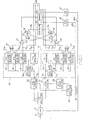
- a demodulator for use in a four-by-four quadrature amplitude modulation system, namely, 16-QAM system. It is readily understood under the circumstances that k and N are equal to four and two, respectively.
- the demodulator comprises a gain controllable amplifier 15 supplied with an intermediate frequency signal IF which is subjected to the above-mentioned QAM and which may be called a demodulator input signal.
- the gain controllable amplifier 15 is also supplied with an automatic gain control signal (AGC) produced in a manner to be later described. As a result, the amplifier 15 produces a gain controlled signal.
- AGC automatic gain control signal
- the gain controlled signal has a first and a second phase component having a quadrature phase difference relative to each other and a first and a second input level, respectively.
- Each of the first and the second input levels is variable between a first predetermined level and a k-th, namely, a fourth predetermined level lower than the first predetermined level.
- each of the first and the second input levels is put into a specific one of the first through the k-th predetermined levels.
- The-first through the k-th predetermined levels may be called first through k-th successively descending levels, respectively.
- the gain controlled signal is delivered through a first signal separator or a first splitter 17 to first and second phase detectors 21 and 22 each of which carries out coherent detection of the gain controlled signal with reference to a first reference carrier signal and a second reference carrier signal having a quadrature phase difference relative to the first reference carrier signal.
- the demodulator comprises a voltage-controlled oscillator 24 responsive to an automatic phase control signal APC (to be later detailed) for producing a local oscillation signal.
- APC automatic phase control signal
- the local oscillation signal is divided through a second spliter 26 into two parts one of which is given through a x/2- phase shifter 28 to the first phase detector 21 as the first reference carrier signal and the other of which is given to the second phase detector 22 as the second reference carrier signal.
- a combination of the first and the second phase detectors 21 and 22, the voltage-controlled oscillator 24, the second splitter 26, and the n/2-phase shifter 28 serves to carry out the coherent detection and may therefore be called a coherent detection circuit.
- the first and the second phase detectors 21 and 22 produce first and second detection signals Xp and X Q .
- the first and the second detection signals Xp and X Q have first and second detection levels corresponding to the first and the second input levels, respectively. Therefore, each of the first and the second detection levels takes one of first through k-th, namely, fourth prescribed levels LV , LV 2 , LV 3 , and LV 4 (shown by solid lines) corresponding to the first through the fourth successively descending levels, respectively.
- a median level ML is provided between the first and the fourth prescribed levels. The median level is different from the first through the k-th prescribed levels. It is assumed that a level distance between two adjacent ones of the first through the fourth prescribed levels is constant. It is readily understood that the first and the second prescribed levels are symmetric to the fourth and the third prescribed levels on both sides of the median level.
- the first and the second detection signals Xp and X Q are supplied to first and second processing circuits 31 and 32 for processing the first and the seoond detection signals Xp and X Q , respectively.
- the first processing circuit 31 produces a first set of binary signals D p1 and Dp 2 and a first additional binary signal in a manner to be described later.
- the seconsd processing circuit 32 produces a second set of binary signals D Q1 and D Q2 and a second additional binary signal.
- each of the first and the secoond additional binary signals consists of a pair of partial bit signals E PL (E QL ) and E PU (E QU ) as will later be described in detail.
- the partial bit signals E PL and E PU may be referred to as first and second partial bit signals, respectively, while the partial bit signals E QL and E QU , third and fourth partial bit signals, respectively.
- the Fifss ese or one Binery sigmis Dp1 Asd Dfk is representative of the first detection level of the first detection signal Xp while the second set of the binary signals D Q1 and D Q2 , the second detection level of the seoond detection signal X Q . Therefore, a combination of the first and the second sots is produced as demodulated signals DM.
- the first-set binary signals D P1 and D P2 may be called a first most significant bit signal and a first less significant bit signal, respectively, while the second-set binary signals D Q1 and D Q2 , a second most significant bit signal and a second less significant bit signal, respectively,
- Such first and second processing circuits may be analog-to-digital converters.
- use of the analog-to-digital converters results in an increase of costs, as pointed out in the preamble of the instant specification.
- the first processing circuit 31 illustrated in Fig. 1 comprises a first binary detector 34 having a first reference level equal to the median level ML. Responsive to the first detection signal Xp, the first binary detector 34 produces the first most significant bit signal DPi that represents whether or not the first detection level is higher than the first reference level.
- the first processing circuit 31 comprises a full-wave rectifier 35 responsive to the first detection signal Xp.
- the full-wave rectifier 35 has a rectifying level equal to the median level ML and carries out full-wave rectification of the first detection signal X P in relation to the rectifying level to produce a rectified signal X PA .
- the rectified signal X PA is like the first detection signal X P folded relative to the rectifying level (ML), is illustrated in Fig. 2(B) and, therefore, has a rectified level determined by the first detection signal X p . More specifically, the rectified level is variable between a low rectified level LL and a high rectified level HL.
- the low rectified level LL corresponds to the second and the third prescribed levels LV 2 and LV 3 while the high rectified level HL, the first and the fourth prescribed levels LV1 and LV .
- the full-wave rectifier 35 may be called a first rectifying circuit.
- the rectified signal X PA is given to'a first elementary binary detector 36 and moreover to first and second additional binary detectors 37 and 38 all of which are operable to derive, from the rectified signal X PA , the first less significant bit signal D P2 and the first and the second partial bit signals E PL and E PU .
- the first elementary binary detector 36 has a first elementary reference level AL 1 (Fig. 2(B)) between the low and the high rectified levels LL and HL. It is to be noted here that the first elementary reference level AL 1 is different from both of the low and the high rectified levels LL and HL. This means that the first elementary reference level ALl corresponds to both levels (shown by dashed lines in Fig. 2(A)) between the first and the second prescribed levels LV 1 and LV 2 and between the third and the fourth prescribed levels LV 3 and LV 4 .
- the first elementary binary detector 36 detects whether or not the rectified level is higher than the first elementary reference level AL 1 and produces the first less significant bit signal D P2 .
- the first less significant bit signal D P2 may be referred to as a first subordinate bit signal.
- a combination of the first reference level and the first elementary reference level AL 1 enables discrimination of the first through the fourth prescribed levels LV1 to LV4 . It is therefore readily understood that the first-set binary signals D P1 and D P2 serve as a part of the demodulated signals DM, as mentioned before.
- the first additional binary detector 37 has a first additional reference level equal to the low rectified level LL when no variation takes place in the rectified signal X PA .
- the first additional reference level corresponds to both of the second and the third prescribed levels LV 2 and LV 3 shown in Fig. 2(A).
- the first additional binary detector 37 detects whether or not the rectified level is higher than the first additional reference level and produces the first partial bit signal E PL as a result of the detection.
- the first partial bit signal E PL may be referred to as a second subordinate bit signal.
- the second additional binary detector 38 has a second additional reference level equal to the high rectified level HL when no variation occurs in the rectified signal X PA .
- the second additional reference level corresponds to both of the first and the fourth prescribed levels LV 1 and LV 4 illustrated in Fig. 2(A).
- the second binary detector 38 Supplied with the rectified signal X PA , the second binary detector 38 produces the second partial bit signal E PU that represents whether or not the rectified signal X PA is higher than the second additional reference level.
- the second partial bit signal E PU may be called a third subordinate bit signal.
- a combination of the first elementary binary detector 36 and the first and the second additional binary detectors 37 and 38 may be referred to as a first discriminating circuit.
- the first processing circuit 31 comprises a combination of four binary detectors 34, 36, 37, and 38 and a single full-wave rectifier 35 and can divide the first detection level ( XPA ) into first through eighth level. zones Z 1 to Z 8 , as shown in Fig. 2(A).
- four levels of the first detection signal X PA can be specified by the first through the eighth level zones Z 1 to Z 8 . This is for detecting variation of the first detection level, as will become clear as the description proceeds.
- the second processing circuit 32 is similar in operation and in structure to the first processing circuit 31 except that the second processing circuit 32 is put into operation in response to the second detection signal X Q to produce the second set of the binary signals D Q1 and D Q2 and the second additional binary signal (E QL and E QU ) by the use of a rectified signal X QA internally produced in the second processing circuit 32.
- the second processing circuit 32 comprises a second binary detector 42, a full-wave rectifier 43, a second elementary binary detector 46, and third and fourth additional binary detectors 47 and 48.
- the full-wave rectifier 43 may be referred to as a second rectifying circuit and a combination of the second elementary binary detector 46 and the third and the fourth additional binary detectors 47 and 48 may be called a second discriminating circuit.
- a circuit arrangement is coupled to the first and the second processing circuits 31 and 32 to derive the automatic phase control signal APC and the automatic gain control signal AGC from the first and the second sets of the binary signals D P1 , D P2 ; and D Q1 , D Q2 and the first and the second additional binary signals (E PL , E ?U ; E QL , E QU ).
- the circuit arrangement comprises a first Exclusive OR circuit 51 supplied as the first additional binary signal with the first and the second partial bit signals E PL and E PU and a second Exclusive OR circuit 52 coupled to the first Exclusive OR circuit 51 and supplied with the first less significant bit signal D p 2.
- a pair of the first and the second Exclusive OR circuits 51 and 52 produce a first internal signal Y P1 given by:
- a first Exclusive NOR circuit 53 is supplied with the first internal signal Y P1 and the first most significant bit D P1 to produce a second internal signal Y P2 given by:
- third and fourth Exclusive OR circuits 56 and 57 produce a third internal signal Y Q1 given by: and a second Exclusive NOR circuit 58 carries out an Exclusive NOR operation to produce a fourth internal signal Y Q2 given by:
- the first through the fourth internal signals Y P1 , Y P2 , Y Q1 and YQ2 are determined by the first through the eighth level zones Z 1 to Z 8 for each of the first and the second detection signals X P and X Q .
- Table 1 shows a truth table which gives relationships between the level zones Z 1 to Z 8 and the above-mentioned various signals D P1 , D P2 , E PL , E PU , Y P1 , and Y P2 or D Q1 , D Q2 , E QL, E QU , Y Q1 , and Y Q2 .
- the first and the third internal signals Y P1 and Y Q1 serve to produce the automatic gain control signal AGC. More specifically, logic levels in the first through the fourth level zones Z to Z 4 for each of the first and the third internal signals Y P1 and Y Ql are reverse in polarity to the logic levels in the fifth through the eighth level zones Z 5 to Z 8 therefor, respectively. This means that variation or fluctuation of each of the first and the second detection signal X P and X Q can be specified by the use of the first and the third internal signals Y P1 and Y Q1 .
- an adder 60 sums up the first and the third internal signals Y P1 and Y Q1 to supply the automatic gain control signal AGC through a first low pass filter 61 to the gain controllable amplifier 15. Either one of the first and the third internal signals Y P1 and YQl may be supplied as the automatic gain control signal AGC to the amplifier 15 through the first low pass filter 61.
- each of the second and the fourth internal signals Y P2 and Y Q2 has the logic "0" levels in every other one of the first through the eighth level zones Z1 to Z 8 and the logic "1" levels in the remaining level zones, as shown in Table 1.
- such signals serve to produce the automatic phase control signal APC because the automatic phase control signal APC is given by:
- the circuit arrangement comprises a fifth Exclusive OR circuit 65 responsive to the second internal signal Y P2 and the second most significant bit signal D Ql and a sixth Exclusive OR circuit 66 responsive to the fourth internal signal Y Q2 and the first most significant bit signal.
- the fifth Exclusive OR circuit 65 produces a first product signal A 1 represented by Y P2 ⁇ D Q1 while the sixth Exclusive OR circuit 66, a second product signal A represented by Y Q2 ⁇ D P1 .
- a subtractor 68 Supplied with the first and the second product signals A 1 and A 2 , a subtractor 68 carries out subtraction shown by the formula (5) -to produce a difference signal representative of a difference between Y Q2 ⁇ D P1 and Y P2 ⁇ D Q1 .
- the difference signal is supplied as the automatic gain control signal AGC to the voltage-controlled oscillator 24 through a second low pass filter 69.
- the demodulator illustrated in Fig. 1 is capable of concurrently producing the automatic gain control signal AGC and the automatic phase control signal APC without any analog-to-digital converters. In addition, it is unnecessary to use any multipliers unstable in characteristics and intricate in structure. The demodulator is therefore inexpensive. An eye aperture appearing in an eye pattern after demodulation is kept substantially constant because of production of the automatic gain control signal AGC and absence of multipliers.
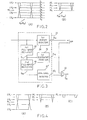
- a demodulator according to a second emboaiment of this invention is represented by a first processing circuit 31 because a second processing circuit 32 is similar to the first processing circuit 31 and the other parts are similar to those illustrated in Fig. 1 except that the first Exclusive OR circuit 51 is removed from Fig. 3.
- the first processing circuit 31 comprises the first binary detector 34 and the full-wave rectifier 35, and the elementary binary detector 36 similar to those illustrated in Fig. 1.
- a single additional binary detector 37' alone is included in the first processing circuit 31.
- the illustrated full-wave rectifier 35 will be referred to as a first full-wave rectifier.
- the first full-wave rectifier 35 has the rectifying level equal to the median level ML (Fig. 4(A)), as is the case with the full-wave rectifier illustrated in Fig. 1.
- the rectifying level may be called a first rectifying level.
- the first full-wave rectifier 35 carries out full-wave rectification in relation to the first rectifying level to produce the rectified signal X PA (will be referred to as a first rectified signal) having the rectified level variable between the low rectified level LL and the high rectified level HL, both inclusive, as illustrated in Fig. 4(B).
- the first rectified signal X PA is supplied to a second full-wave rectifier 72 having a second rectifying level RL intermediate between the high and the low rectified levels HL and LL, as shown in Fig. 4(B).
- the second full-wave rectifier 72 carries out full-wave rectification in relation to the second rectifying level RL to produce a second rectified signal X PB having an additional rectified level depicted by a solid line in Fig. 4(C).
- the additional rectified level corresponds to the first through the fourth prescribed levels LV 1 , LV 2 , LV 3 , and LV 4 and is variable with reference to a preselected level PL.
- the first through the fourth prescribed levels LV , LV2, LV 3 , and LV 4 are converted into a single level by the use of the first and the second full-wave rectifiers 35 and 72.
- a combination of the first and the second full-wave rectifiers 35 and 72 serves as a first rectifying circuit.
- the first rectified signal X PA is given to the first elementary binary detector 36 to be processed in the manner described with reference to Fig. 1.
- the first elementary binary detector 36 produces the first less significant bit signal D P2 as a first subsidiary bit signal.
- the second rectified signal X PB is sent to the additional binary detector 37' having a secondary reference level equal to the preselected level PL.
- the additional binary detector 37' detects whether or not the additional rectified level is higher than the secondary reference level (PL) and produces a second subsidiary bit signal as the first additional binary signal depicted at AD 1 .
- the first detection level is divided into first through eighth level zones, as is the case with the first processing circuit 31 illustrated in Fig. 1 and that a combination of the first set of the binary signals and the first additional binary signal AD 1 can specify each of the first through the eighth level zones.
- the circuit arrangement comprises the second Exclusive OR circuit 52 responsive to the first less significant bit signal D P2 and the first additional bit signal AD for carrying out an Exclusive OR operation to produce a first internal signal.
- the first internal signal is identical with that illustrated with reference to Fig. 1, as will presently become clear, and is therefore depicted at Y P1 in Fi g . 3.
- the first internal signal Y P1 is delivered to the first Exclusive NOR circuit 53 (Fig. 1) to produce the second internal signal Y P2 and to the adder 60 (Fig. 1).
- the second processing circuit 32 produces the second set of the binary signals D Ql and D Q2 and the second additional binary signal D Q3 in the above-mentioned manner.
- the fourth Exclusive OR gate 57 (Fig. 1) is supplied with the second additional binary signal D Q3 and the second less significant bit signal DQ2 to produce the third internal signal Y Q1 .
- the second Exclusive NOR circuit 58 produces the fourth internal signal Y Q2 in response to the third internal signal Y Q1 and the most significant bit signal D Q1.
- Table 2 shows a truth table which is similar to Table 1 and which gives the relationships between the first through the eighth level zones and the above-mentioned signals.
- each of the first and the third internal signals Y P1 and Y Q1 serves to produce the automatic gain control signal AGC while the second and the fourth internal signals Y P2 and Y Q2 , the automatic phase control signal APC, as described in conjunction with Table 1.
- a demodulator for use in an eight-by-eight quadrature amplitude modulation system, namely, 64-QAM system.
- the numbers k and N are equal to 8 and 3, respectively.
- Each of the first and the second detection signals X P and X Q is variable between first and eighth prescribed levels LV 1 and LV 8 , both inclusive, as illustrated in Fig. 6(A).
- the first and the eighth prescribed levels may be referred to as the highest and the lowest levels, respectively.
- a median level ML is provided between the first and the eighth prescribed levels LV 1 and LV 8 , as illustrated in Fig. 6(A).
- the illustrated demodulator is implemented by modifying the demodulator illustrated in Fig. 1 and comprises similar parts designated by like reference numerals. It is, however, to be noted that the first and the second processing circuits 31 and 32 are somewhat different from those illustrated in Fig. 1 in order to define first through sixteenth level zones Z 1 to Z16 in which each of the first and the second detection signals X P and X Q is variable. In this connection, a circuit arrangement is also different from that illustrated in Fig. 1.
- the first processing circuit 31 comprises the first binary detector 34 for producing the first most significant bit signal DPi and a pair of full-wave rectifiers 35 and 72 which are connected in cascade and which will be called first and second full-wave rectifiers, as is the case with Fig. 3.
- the first full-wave rectifier 35 has a first rectifying level RL 1 equal to the median level ML and produces the first rectified signal X PA as shown in Fig. 6(B) after carrying out full-wave rectification of the first detection signal X P in relation to the first rectifying level RL 1 .
- the first rectified signal X PA has a first rectified level taking a preselected one of first, second, third and fourth levels successively descending as depicted at solid lines in Fig. 6(B).
- the second full-wave rectifier 72 has a second rectifying level RL 2 predetermined between the second and the third levels of the first rectified signal X PA and carries out full-wave rectification of the first rectified signal X PA in relation to the second rectifying level to produce a second rectified signal X PB .
- the second rectified signal X PB has a second rectified level taking one of high and low levels HL and LL as shown in Fig. 6(C).
- a combination of the first and the second full-wave rectifiers 35 and 72 is operable to derive, from the first detection signal X P , a rectified signal of two levels, such as the second rectified signal. It is readily understood that the number of the full-wave rectifiers may be equal to (N - 1), in order to produce the rectified signal of two levels.
- the first processing circuit 31 comprises first and second elementary binary detectors 76 and 77 responsive to the first and the second rectified signals X PA and X PB for producing, as the remaining part of the first-set binary signals, first less and first least significant bit signals D P2 and D P3 , respectively.
- the first less and the first least significant bit signals D P2 and D P3 are produced together with the first most significant bit signal DPi as a part of the demodulated signals DM.
- the first elementary binary detector 76 has a first reference level equal to the second rectifying level RL 1 and compares the first rectified level with the first reference level to produce the first less significant bit signal D P2 as a result of the comparison.
- the second elementary binary detector 77 has a second reference level RE between the high and the low rectified levels HL and LL as illustrated in Fig. 6(C) and produces the first least significant bit signal D P3 after comparison of the second rectified siganl XF B with the second reference level RE.
- the number of the elementary binary detectors may be equal to (N - 1).
- the first processing circuit 31 further comprises first and second auxiliary binary detectors 78 and 79 supplied with the second rectified signal X PB .
- the first and the second auxiliary binary detector 78 have first and second auxiliary reference levels equal to the low rectified level LL and the high rectified level HL, respectively, as long as the second rectified level is invariable.
- Each of the first and the second auxiliary binary detectors 78 and 79 detects whether or not the second rectified level is higher than each of the first and the second auxiliary reference levels and produces each of first and second partial bit signals E PL and E PU as the additional binary signal.
- the second elementary binary detector 77 and the first and the second auxiliary binary detectors 78 and 79 are similar in operation to the elementary binary detector 36 and the first and the second additional binary detectors 37 and 38 illustrated in Fig. 1, respectively.
- a combination of the first and the second full-wave rectifiers 35 and 72 may be called a first rectifying circuit while the first and the second elementary binary detectors 76 and 77 may be referred to as a first discriminating circuit together with the first and the second auxiliary binary detectors 78 and 79.
- the second processing circuit 32 is similar in operation and structure to the first processing circuit 31 and therefore comprises the second binary detector 42, a second rectifying circuit, and a second discriminating circuit.
- the second-rectifying circuit comprises third and fourth full-wave rectifiers for producing third and fourth rectified signals X QA and X QB in a manner described in conjunction with the first and the second full-wave rectifiers 35 and 72.
- the second discriminating circuit comprises third and fourth elementary binary detectors 83 and 84 similar to the first and the second elementary binary detectors 76 and 77, respectively, and third and fourth auxiliary detectors 86 and 87 also similar to the first and the second auxiliary binary detectors 78 and 79, respectively.
- the second processing circuit 32 produces the second-set binary signals D Q1 , D Q2 , and D Q3 and the second additional binary signal which is a combination of third and fourth partial bit signals E QL and E QU .
- the circuit arrangement is similar to that illustrated in Fig. 1 except that first and second additional Exclusive OR circuits 91 and 92 are added to the illustrated circuit arrangement.
- the first additional Exclusive OR circuit 91 is connected to the first and the second elementary binary detectors 76 and 77 and the second Exclusive OR circuit 52 while the second additional Exclusive OR circuit 92 is connected to the third and the fourth elementary binary detectors 76 and 77 and the fourth Exclusive OR circuit 57.
- the first and the third internal signals Y P1 and Y Q1 are given by: and respectively.
- the second and the fourth internal signals Y P2 and Y Q2 are given by: and respectively.
- Table 3 gives the relationships between each of the first through the sixteenth level zones Z 1 to Z 16 and the above-mentioned signals.
- the first and the third internal signals Y P1 and Y Q1 are usable to produce the automatic gain control signal AGC while the second and the fourth internal signals Y P2 and YQ 2 , the automatic phase control signal APC, as described in conjunction with Fig. 1.
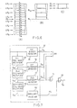
- a demodulator according to a fourth embodiment of this invention is for use in the eight-by-eight quadrature amplitude modulation system, as is the case with Fig. 5, and is implemented by modifying the demodulator illustrated with reference to Fig. 3.
- the first processing circuit 31 alone is illustrated in Fig. 7 because the second processing circuit 32 is similar to the first processing circuit 31 and the remaining portions are similar to those illustrated in Fig. 5 except that the first and the third Exclusive OR circuits 51 and 56 are removed from the circuit arrangement illustrated in Fig. 7.
- the illustrated first processing circuit 31 is similar to that illustrated in Fig. 5 except that a first additional full-wave rectifier 93 is attached to the second full-wave rectifier 72 and a single auxiliary binary detector 94 alone is used instead of the first and the second auxiliary binary detectors 78 and 79.
- the number of the full-wave rectifiers 35, 72, and 93 is rendered equal to N.
- the number of the binary detectors 34, 76, 77, and 94 becomes equal to (N + 1).
- the first additional full-wave rectifier 93 has a first additional rectifying level equal to the second reference level RE shown in Fig. 6(C) and full-wave rectifies the second rectified signal X PB in relation to the first additional rectifying level to produce a first additional rectified signal X PC having a first additional rectified level as shown in Fig. 4(C).
- the auxiliary binary detector 94 has a reference level equal to the preselected level PL and detects variation of the first additional rectified level in relation to the reference level. A result of detection is produced as the first additional binary signal AD 1 from the auxiliary binary detector 94.
- the first additional binary signal AD 1 is supplied direct to the second Exclusive OR circuit 52 responsive to the second detected signal DP 3 .
- the first output signal Y P1 can be produced as is the case with the first processing circuit 31 illustrated in Fig. 5.
- a pair of partial bit signals F PL (E ) and E PU (EQU) may be produced as the additional binary signal by repeating full-wave rectifications (N - 1)-times to obtain a signal of two levels and by discriminating the signal by the use of three binary detectors.
- the additional binary signal may be produced by successively carrying out full-wave rectifications N-times to derive a single level signal from a k-level signal and by comparing the single level signal with a reference level.
- both of the automatic gain control signal and the automatic phase control signal are obtained by processing the additional binary signal.
Landscapes
- Engineering & Computer Science (AREA)
- Computer Networks & Wireless Communication (AREA)
- Signal Processing (AREA)
- Digital Transmission Methods That Use Modulated Carrier Waves (AREA)
Applications Claiming Priority (2)
| Application Number | Priority Date | Filing Date | Title |
|---|---|---|---|
| JP57148526A JPS5939149A (ja) | 1982-08-28 | 1982-08-28 | 多値直交振幅復調器 |
| JP148526/82 | 1982-08-28 |
Publications (3)
| Publication Number | Publication Date |
|---|---|
| EP0104449A2 true EP0104449A2 (de) | 1984-04-04 |
| EP0104449A3 EP0104449A3 (en) | 1984-10-03 |
| EP0104449B1 EP0104449B1 (de) | 1987-05-13 |
Family
ID=15454747
Family Applications (1)
| Application Number | Title | Priority Date | Filing Date |
|---|---|---|---|
| EP83108388A Expired EP0104449B1 (de) | 1982-08-28 | 1983-08-25 | QAM-Demodulator der eine Kombination eines Vollweggleichrichters und binärer Detektoren enthält |
Country Status (5)
| Country | Link |
|---|---|
| US (1) | US4546323A (de) |
| EP (1) | EP0104449B1 (de) |
| JP (1) | JPS5939149A (de) |
| CA (1) | CA1200854A (de) |
| DE (1) | DE3371589D1 (de) |
Cited By (5)
| Publication number | Priority date | Publication date | Assignee | Title |
|---|---|---|---|---|
| EP0135057A1 (de) * | 1983-07-22 | 1985-03-27 | Nec Corporation | Demodulator für ein Mehrpegelamplitudenmoduliertes Signal |
| EP0312047A3 (en) * | 1987-10-14 | 1990-05-30 | Nec Corporation | Analog-to-digital converter for stepped square qam demodulators |
| WO1996014700A3 (en) * | 1994-11-08 | 1996-07-25 | Zenith Electronics Corp | AGC circuit for a digital receiver |
| WO2005060196A1 (en) * | 2003-12-17 | 2005-06-30 | Nec Corporation | Demodulation of a multi-level quadrature amplitude modulation signal |
| RU224777U1 (ru) * | 2023-11-13 | 2024-04-04 | Федеральное государственное бюджетное образовательное учреждение высшего образования "Сибирский государственный университет телекоммуникаций и информатики" | Инвариантный амплитудный демодулятор с двумя опорными сигналами |
Families Citing this family (8)
| Publication number | Priority date | Publication date | Assignee | Title |
|---|---|---|---|---|
| US4901332A (en) * | 1988-10-27 | 1990-02-13 | Unisys Corp. | Noncoherent-coherent A.C. coupled base band AGC receiver |
| RU2198470C1 (ru) * | 2001-09-28 | 2003-02-10 | Государственное конструкторское бюро аппаратно-программных систем "Связь" Всероссийского НИИ "Градиент" | Демодулятор сигналов шестнадцатипозиционной квадратурной амплитудной манипуляции |
| RU2234814C1 (ru) * | 2003-03-19 | 2004-08-20 | Федеральное государственное унитарное предприятие "Государственное конструкторское бюро аппаратно-программных систем "Связь" | Демодулятор сигналов шестнадцатипозиционной квадратурной амплитудной манипуляции |
| RU2246182C1 (ru) * | 2003-07-17 | 2005-02-10 | Федеральное государственное унитарное предприятие "Государственное конструкторское бюро аппаратно-программных систем "Связь" (ФГУП "ГКБ "Связь") | Демодулятор сигналов шестнадцатипозиционной квадратурной амплитудной манипуляции |
| RU2254687C1 (ru) * | 2003-12-29 | 2005-06-20 | Федеральное государственное унитарное предприятие "Государственное конструкторское бюро аппаратно-программных систем "Связь" (ФГУП "ГКБ "Связь") | Устройство восстановления несущей частоты шестнадцатипозиционной квадратурной амплитудной манипуляции |
| RU2291583C1 (ru) * | 2005-07-19 | 2007-01-10 | Федеральное государственное унитарное предприятие "Государственное конструкторское бюро аппаратно-программных систем "Связь" (ФГУП "ГКБ "Связь") | Демодулятор сигналов шестнадцатипозиционной квадратурной амплитудной манипуляции |
| JP5281530B2 (ja) * | 2009-09-29 | 2013-09-04 | ルネサスエレクトロニクス株式会社 | 復調器 |
| US11175394B2 (en) | 2019-03-27 | 2021-11-16 | Raytheon Company | Binary to quad phase generator |
Family Cites Families (5)
| Publication number | Priority date | Publication date | Assignee | Title |
|---|---|---|---|---|
| JPS5716546B2 (de) * | 1973-07-12 | 1982-04-06 | ||
| JPS5918900B2 (ja) * | 1976-03-22 | 1984-05-01 | 日本電気株式会社 | 復調装置 |
| JPS5384670A (en) * | 1976-12-29 | 1978-07-26 | Nec Corp | Demodulating system for multilevel carrier digital signal |
| JPS57131151A (en) * | 1981-02-06 | 1982-08-13 | Nec Corp | Carrier wave reproducing circuit |
| JPS57131152A (en) * | 1981-02-06 | 1982-08-13 | Nec Corp | Automatic gain controlling circuit |
-
1982
- 1982-08-28 JP JP57148526A patent/JPS5939149A/ja active Granted
-
1983
- 1983-08-25 DE DE8383108388T patent/DE3371589D1/de not_active Expired
- 1983-08-25 EP EP83108388A patent/EP0104449B1/de not_active Expired
- 1983-08-29 CA CA000435511A patent/CA1200854A/en not_active Expired
- 1983-08-29 US US06/527,621 patent/US4546323A/en not_active Expired - Lifetime
Cited By (7)
| Publication number | Priority date | Publication date | Assignee | Title |
|---|---|---|---|---|
| EP0135057A1 (de) * | 1983-07-22 | 1985-03-27 | Nec Corporation | Demodulator für ein Mehrpegelamplitudenmoduliertes Signal |
| EP0312047A3 (en) * | 1987-10-14 | 1990-05-30 | Nec Corporation | Analog-to-digital converter for stepped square qam demodulators |
| WO1996014700A3 (en) * | 1994-11-08 | 1996-07-25 | Zenith Electronics Corp | AGC circuit for a digital receiver |
| CN1110175C (zh) * | 1994-11-08 | 2003-05-28 | 齐尼思电子公司 | 用于数字电视接收机的自动增益控制电路及方法 |
| WO2005060196A1 (en) * | 2003-12-17 | 2005-06-30 | Nec Corporation | Demodulation of a multi-level quadrature amplitude modulation signal |
| CN1894919B (zh) * | 2003-12-17 | 2010-08-18 | 日本电气株式会社 | 对多水平正交调幅信号的解调 |
| RU224777U1 (ru) * | 2023-11-13 | 2024-04-04 | Федеральное государственное бюджетное образовательное учреждение высшего образования "Сибирский государственный университет телекоммуникаций и информатики" | Инвариантный амплитудный демодулятор с двумя опорными сигналами |
Also Published As
| Publication number | Publication date |
|---|---|
| DE3371589D1 (en) | 1987-06-19 |
| EP0104449A3 (en) | 1984-10-03 |
| CA1200854A (en) | 1986-02-18 |
| US4546323A (en) | 1985-10-08 |
| JPS5939149A (ja) | 1984-03-03 |
| EP0104449B1 (de) | 1987-05-13 |
| JPS6362934B2 (de) | 1988-12-05 |
Similar Documents
| Publication | Publication Date | Title |
|---|---|---|
| EP0104449A2 (de) | QAM-Demodulator der eine Kombination eines Vollweggleichrichters und binärer Detektoren enthält | |
| US4875049A (en) | Automatic level control circuit for an ad convertor | |
| US5134634A (en) | Multilevel quadrature amplitude demodulator capable of compensating for a quadrature phase deviation of a carrier signal pair | |
| US20050089120A1 (en) | FSK demodulator system and method | |
| CA1224542A (en) | Demodulator for multilevel amplitude modulation system | |
| GB2166324A (en) | A multi-mode radio transceiver | |
| CA1192615A (en) | Carrier recovery circuit | |
| US4574246A (en) | Demodulator with AGC circuit for multi-level quadrature amplitude-modulated carrier wave | |
| US5519733A (en) | Method and apparatus for recovering a qam carrier | |
| US6038268A (en) | Direct conversion FSK signal radio receiver | |
| EP0118119B1 (de) | Taktsynchronisierungsschaltung | |
| US4574244A (en) | QAM Demodulator automatic quadrature loop using n-m LSB's | |
| US4571550A (en) | QAM Demodulator carrier recovery loop using n-m LSB's | |
| US4823361A (en) | Interference immune digital modulation receiver | |
| EP0106163B1 (de) | Demodulator für ein phasenumgetastetes Signal mit acht Phasenlagen | |
| EP0083236B1 (de) | Schaltung zur Trägerrückgewinnung | |
| US4517680A (en) | Error vector normalizer | |
| US4881049A (en) | QAM modulator/demodulator | |
| CA1162244A (en) | Digital data transmission systems | |
| CA1283710C (en) | Interference immune digital modulation receiver | |
| EP0721270A1 (de) | Direktmisch-Empfänger für mehrstufige FSK-Signale | |
| GB2063629A (en) | Digital data transmission systems | |
| JPS6366108B2 (de) | ||
| JPS62233942A (ja) | 干渉補償回路 | |
| GB2124046A (en) | Data demodulator for a direct frequency modulated signal |
Legal Events
| Date | Code | Title | Description |
|---|---|---|---|
| PUAI | Public reference made under article 153(3) epc to a published international application that has entered the european phase |
Free format text: ORIGINAL CODE: 0009012 |
|
| 17P | Request for examination filed |
Effective date: 19831111 |
|
| AK | Designated contracting states |
Designated state(s): DE FR GB IT |
|
| PUAL | Search report despatched |
Free format text: ORIGINAL CODE: 0009013 |
|
| AK | Designated contracting states |
Designated state(s): DE FR GB IT |
|
| GRAA | (expected) grant |
Free format text: ORIGINAL CODE: 0009210 |
|
| AK | Designated contracting states |
Kind code of ref document: B1 Designated state(s): DE FR GB IT |
|
| REF | Corresponds to: |
Ref document number: 3371589 Country of ref document: DE Date of ref document: 19870619 |
|
| ET | Fr: translation filed | ||
| ITF | It: translation for a ep patent filed | ||
| PLBE | No opposition filed within time limit |
Free format text: ORIGINAL CODE: 0009261 |
|
| STAA | Information on the status of an ep patent application or granted ep patent |
Free format text: STATUS: NO OPPOSITION FILED WITHIN TIME LIMIT |
|
| 26N | No opposition filed | ||
| ITTA | It: last paid annual fee | ||
| REG | Reference to a national code |
Ref country code: GB Ref legal event code: IF02 |
|
| PGFP | Annual fee paid to national office [announced via postgrant information from national office to epo] |
Ref country code: FR Payment date: 20020808 Year of fee payment: 20 |
|
| PGFP | Annual fee paid to national office [announced via postgrant information from national office to epo] |
Ref country code: GB Payment date: 20020821 Year of fee payment: 20 |
|
| PGFP | Annual fee paid to national office [announced via postgrant information from national office to epo] |
Ref country code: DE Payment date: 20020829 Year of fee payment: 20 |
|
| PG25 | Lapsed in a contracting state [announced via postgrant information from national office to epo] |
Ref country code: GB Free format text: LAPSE BECAUSE OF EXPIRATION OF PROTECTION Effective date: 20030824 |
|
| REG | Reference to a national code |
Ref country code: GB Ref legal event code: PE20 |