EP0104229B1 - Planar ac plasma display having glow suppressor electrode - Google Patents
Planar ac plasma display having glow suppressor electrode Download PDFInfo
- Publication number
- EP0104229B1 EP0104229B1 EP83901276A EP83901276A EP0104229B1 EP 0104229 B1 EP0104229 B1 EP 0104229B1 EP 83901276 A EP83901276 A EP 83901276A EP 83901276 A EP83901276 A EP 83901276A EP 0104229 B1 EP0104229 B1 EP 0104229B1
- Authority
- EP
- European Patent Office
- Prior art keywords
- conductors
- glow
- conductor
- pad
- electrode
- Prior art date
- Legal status (The legal status is an assumption and is not a legal conclusion. Google has not performed a legal analysis and makes no representation as to the accuracy of the status listed.)
- Expired
Links
Images

Classifications
-
- H—ELECTRICITY
- H01—ELECTRIC ELEMENTS
- H01J—ELECTRIC DISCHARGE TUBES OR DISCHARGE LAMPS
- H01J17/00—Gas-filled discharge tubes with solid cathode
- H01J17/38—Cold-cathode tubes
- H01J17/48—Cold-cathode tubes with more than one cathode or anode, e.g. sequence-discharge tube, counting tube, dekatron
- H01J17/49—Display panels, e.g. with crossed electrodes, e.g. making use of direct current
- H01J17/492—Display panels, e.g. with crossed electrodes, e.g. making use of direct current with crossed electrodes
Definitions
- This invention relates to planar ac plasma displays and more particularly to apparatus for preventing glow spreading in such displays.
- all the electrodes are disposed on one substrate, typically a glass plate.
- the electrodes are typically embedded within a dielectric layer disposed on the glass plate.
- the row and column electrodes can be embedded at lower and upper levels respectively, with a dc isolated conductive pad electrode at the upper level located above and capacitively coupled to the lower row electrode.
- a display site or glow cell is formed on the top surface of the dielectric located between the conductive pad and the column electrode. When biased by placing the proper voltages on the appropriate column and row address electrodes, the display gas located over the display cell ionizes creating a glow.
- display cell apparatus comprises a dielectric layer, an enclosed body of ionizable gas adjacent the dielectric layer, a first plurality of conductors embedded in the layer, a second plurality of conductors embedded in the layer forming a plurality of display cells with the first plurality of conductors, and a plurality of individual glow suppression pads for suppressing glow spread approximately equally capacitively coupled to conductors of the first and second plurality of conductors for biasing each suppression pad at a voltage intermediate the voltage on the conductors coupled thereto.
- a glow suppression pad When utilized with the above-identified patented display cell, a glow suppression pad is locafed at the same level as the column electrode opposite the conductive pad electrode.
- the glow suppression pad When a glow suppression pad is utilized with a two-element display cell formed by an upper level column electrode and a lower level row electrode, the glow suppression pad is located adjacent the upper level column electrode. In both applications, the glow suppression pad has a predetermined width and is located a predetermined distance from the upper level electrode.
- the glow suppression pad is capacitively coupled, approximately equally, to both the lower level row electrode and the upper level column electrode using one or to lower level supplementary conductive pads. As a result the glow suppression pad is capacitively biased at a voltage midway between the dc voltage on the lower level row electrode and the upper level column electrode. Thus, the resultant electric field in the display gas between the column electrode and the conductive pad electrode is insufficient to ionize the display gas.
- glow suppression pads are used to prevent unwanted glow at a crossover formed by a row and column electrode.
- the glow suppression pads are located in parallel with and on both sides of the upper level column electrode.
- FIG. 1 of the drawings there is illustrated a perspective view of a display cell of a planar ac plasma display apparatus embodying the invention.
- the partial cutaway view permits a clear view of the electrodes (used interchangeably herein with the word conductors) of an individual display cell (site) and includes a substrate 100 and dielectric layer 101.
- a cover plate covers dielectric layer 101 and encloses a body of ionizable gas between it and the surface 109 of dielectric layer 101.
- the ionizable gas may be, for example, a mixture of neon and one-tenth percent argon at a pressure of 65,000 Pa (500 Torr).
- both the cover plate and substrate 100 are a glass plate.
- the dielectric material can be any of a variety of well-known materials such as, for example, Electro-Science Labs M4111C.
- Individual display cell or display site DS comprises three elements (electrodes) and is formed by the intersection of row electrode 103 and column electrode 102 and includes glow supporting conductive pad 104.
- the location of column electrode 102 and glow supporting pad 104 are at the upper level, being somewhat above the lower level of row electrode 103.
- gas ionization occurs generally in the area of dielectric surface 109 between edge 110 of glow supporting pad 104 and edge 111 of column conductor 102.
- Conductive pads 107 and 108 and glow suppression pad 106 of the present invention are also part of display cell DS and are utilized to limit and/ or prevent unwanted gas ionization.
- An ac plasma display consists of a matrix of the previously described display cells DS formed by the intersection of row and column electrodes (conductors) with each cell including an associated glow supporting pad. While display cell DS typically includes the intersection of a row and column conductor it is to be understood that a display cell could include two conductors which do not crossover but become more proximate to each other at a display cell location. In such an arrangement, the conductors need not be embedded in the dielectric at different levels but could be located at the same level.
- the basic construction and operation of the three-element display cell DS of FIG. 1 is similar to that of the display cell described in U.S. Patent No. 4,164,678.
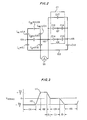
- FIG. 2 shows capacitive equivalent circuit of display cell DS.
- the capacitances 112 through 117 are associated with the operation of the disclosed inventive glow suppression pad or pads and will be discussed in a later paragraph.
- the remaining capacitances in the equivalent circuit represent the capacitance between respective pairs of points in the display cell.
- the equivalent circuit also includes a signal source, SS, illustratively a write voltage source, connected between the row and column conductors.
- capacitance C o is made large by forming row conductor 103 such that it has a widened region or pad, 103a, which lies directly below, and may illustratively be the same shape as, pad 104.
- Typical values for the capacitances of the equivalent circuit are shown in FIG. 2. These values are rough calculations arrived at assuming the following physical parameters: Width of conductors 102 and 103, 0.003"; size of pads 103a and 104 is 0.010" by 0.010"; width of the gap between conductor 102 and pad 104, 0.003"; total thickness of dielectric layer 101, 0.002"; and distance between upper and lower electrode levels within dielectric layer 101, 0.0015".
- capacitances C W1 and C W2' which vary as a function of the amount of wall charge stored, are given at their approximate values.
- the equivalent capacitance of the network comprised of capacitances Cg d , C w1 , C W2 and Cgg is substantially equal to the value of capacitance Cg d , which in this example is approximately 0.015 pf.
- the value of capacitance C o is approximately ten times greater than that of capacitance Gg d .
- Display cell DS is selected or addressed for operation by application of a write voltage pulse (SS of FIG. 2) across row conductor 103 (and hence pad 104) and column conductor 102.
- the write voltage pulse (SS) for display cell DS may be generated by applying the voltage pulses +Vw/2 and -Vw/2 to conductors 103 and 102, respectively. Note, however that all the pads (104, 105, etc.) of display cells along row conductor 103 receive a +Vw/2 voltage pulse and that all display cells along column conductor 102 receive a -Vw/2 voltage pulse.
- a display cell requires a write voltage pulse of Vw, only display cell DS located at the intersection of row conductor 103 and column conductor 102 will ignite and produce a light-emitting (ON) glow.
- the discharge and glow of display cell DS occurs between pad 104 and column conductor 102 in a well-known manner.
- the glow appears in the ionized gas on the dielectric surface between edges 110 of pad 104 and edge 111 of column conductor 102.
- a display cell requires further successive sustaining voltage pulses to produce a continuous light-emitting glow.
- the sustaining ac voltage or bipolar pulses are likewise applied across row conductor 103 (pad 104) and column conductor at a magnitude somewhat less than a write pulse.
- the magnitude of the sustaining pulses are less than a write pulse and are insufficient to initiate a discharge at the other display cells along row conductor 103 and column conductor 102.
- a display cell is switched to non-light-emitting (OFF) state by applying an erase pulse which is insufficient to sustain the display cell in the light-emitting (ON) state.
- the discharge or glow created at an ON display cell of a planar ac plasma panel tends to propagate, or spread away from the gap in response to each sustain pulse.
- the glow between edges 110 and 111 attempts to spread across column conductor 102 to pad 105 of adjacent display cell DS' in the absence of glow suppressor 106.
- glow spread can lead to crosstalk or erroneous ignition of nearby OFF display cells (e.g., DS'). The result is a loss of resolution or definition in the character or graphic being displayed.
- this glow spread is inhibited using an individual capacitively coupled glow suppression pad 106 for each display cell.
- an individual capacitively coupled glow suppression pad 106 for each display cell DS obviates the complexities of the prior art method of interspersing glow suppression electrodes between the existing column conductors and providing connection to a common ground or voltage source.
- the disclosed invention eliminates the substantial additional capacitance that the prior art interspersed glow suppression electrodes produced. This additional capacitance significantly loaded the applied write and sustain pulses.
- Glow suppression pad 106 is rectangular in this embodiment and is located on the same level and in parallel with column conductor 102 and on a side opposite the electrode pad 104.
- Glow suppressor pad 106 is of width d1, which is large enough that a glow will not be established across it.
- Width d1 is chosen to be greater than the Paschen minimum discharge length for a given pressure. As is well known in the art, the Paschen minimum discharge length is defined as the smallest length which will support a discharge for the given gas type and pressure.
- Glow suppression pad 106 is located at a distance d2 from column conductor 102 which is chosen to be smaller than the Paschen minimum, i.e., small enough to prevent much surface field (at the gas and dielectric interface) due to row conductor 103. Glow suppression pad 106 is capacitively coupled in an approximately equal manner to lower level row conductor 103 and the upper level column conductor 102. With reference to FIG. 2 again, the capacitances associated with the glow suppression pad 106 are illustrated. Glow suppression pad 106 is capacitively biased by capacitance CT and capacitor C112 at a voltage approximately midway between the voltages on row conductor 103 and column conductor 102.
- Capacitor 112 represents the capacitive coupling between row conductor 103 and suppressor pad 106.
- Capacitance C117 is the minimal edge capacitance between suppressor pad 106 and column, conductor 102.
- Capacitance C117 is a minimal value (stray capacitance) and does not substantially affect the bias or operation of suppressor pad 106 and is only included herein for completeness. Other stray capacitances which are smaller than capacitance C117 have been excluded from FIG. 2 and the following discussion.
- the capacitances C115/C116 and C114/C113 are formed between the lower level conductive pads 107 and 108 and column conductor 102 and suppressor electrode 106, respectively.
- Capacitances C115/C116 and C114/C113 are designed to provide substantial capacitance coupling between column conductor 102 and suppressor electrode 102, thus enabling the coupling of ac voltages to suppressor electrode 102.
- Conductive pad 107 is capacitively coupled to column conductor 102 (C115) and to suppressor electrode 106 (C116).
- conductive pad 108 is capacitively coupled to column conductor 102 (C114) and to suppressor electrode 106 (C113).
- one conductive pad having the appropriate capacitances could be substituted for conductive pads 107 and 108.
- the total capacitance CT between column electrode 102 and suppressor electrode 106 includes C117 in parallel with both the series combination of C114 and C113 as well as C115 and C116.
- the sizes of row and column conductors 102 and 103, and the separation between the upper and lower metalization levels; the size of suppressor electrode 106 and conductive pads 107 and 108 can be determined, in a straightforward manner, to make the total capacitance CT between suppressor electrode 106 and column conductor 102 equal to the capacitance C112 between suppressor electrode 106 and row conductor 103.
- the voltage divider formed by capacitor C112 and CT causes the ac voltage on suppressor electrode 106 to be approximately half of the sum of the voltages on row conductor 103 and column conductor 102. Since the writing voltages are -Vw/2 and +Vw/2, respectively, the voltage on suppressor electrode 106 would be approximately 0 volts. Obviously, the voltage on suppressor electrode would also be approximately 0 volts during sustaining voltage pulses if these were +Vw/2 and -Vw/2 on the two electrodes, respectively.
- the disclosed suppressor electrode 106 and conductive pads 107 and 108 are arranged in accordance with the present invention so that suppressor electrode 106 is capacitively biased via a conductive pad at a voltage between (ideally midway) the voltages on the two conductors. In such an arrangement the suppressor electrode 106 would also again prevent an ON display cell from ionizing the display gas of an adjacent OFF display cell.
- FIG. 3 illustrates the approximate voltages which appear at the dielectric/gas interface 109 for the display cell arrangement shown in FIG. 1.
- the voltage transitions are shown as varying in a linear manner, which is approximately correct.
- a write voltage pulse of +Vw/2 and -Vw/2 is applied to column and row conductors 102 and 103, respectively.
- the resulting voltage on electrode pad 104 is also -Vw/2.
- the voltage on the surface of dielectric/gas interface 109 above electrode pad 104 is approximately -Vw/2. In the region of the dielectric/gas interface 109 between edge 110 of electrode pad 104 and edge 111 of column conductor 102 the voltage starts increasing toward +Vw/2.
- the voltage remains constant, at 0 volts, across the width of suppressor electrode 106 and then decreases to -Vw/2 at electrode pad 105 of the adjacent display cell.
- a differential voltage of Vw exists between electrode pad 105 and column conductor 102, no spreading occurs since the critical electric field is never exceeded.
- the electric field is below the critical level because the distance d1 + d2 + d3 between column conductor 102 and electrode pad 105 is greater than the Paschen discharge distance.
- the mode of operation of glow supporting pad 104 does inhibit glow spreading, as described in previously-identified U.S. Patent No. 4,164,678, the disclosed suppressor electrode 106 provides significant additional margin against glow spread permitting higher cell density in the display.
- an additional important use of the glow stopping electrode 106 is in thin film dielectric construction of a single substrate plasma panel.
- the back glow the glow between an upper column conductor and a buried row conductor, is not prevented by the thickness of the dielectric layer.
- a glow is possible. Since the thickness of the dielectric layer results in only a minimal voltage drop through the dielectric layer, the result is that all of the row conductor drive potential appears at the dielectric/gas interface surface above the buried row conductor, within a few dielectric thickness widths from the top column conductor. The result is that the gas ionizes and a glow exists across the area of the dielectric surface. Using the disclosed glow suppression techniques such unwanted glows can be prevented.
- FIG. 4 illustrates a crossover formed between row conductor 401 and column conductor 402 located, respectively, on substrate 100 and, within dielectric 101.
- Two glow suppressors electrodes 403 and 404 straddle column conductor 402 at a distance smaller than the Paschen minimum discharge length.
- conductive pads 405 and 406 provide a capacitive coupling between column conductor 402 and glow suppressor electrodes 403 and 404 which is approximately equal to the capacitive coupling between glow suppressor electrodes 403 and 404 and row electrode 401.
- the effect of the resulting capacitive voltage divider is that glow suppressor electrodes 403 and 404 are biased midway between the voltage on row conductor 401 and column conductor 402.
- the resulting voltage difference, during a write pulse applied between row conductor 401 and column conductor 402, between glow suppressor electrodes 403 and 404 and either column conductor 402 or row conductor 401 is approximately Vw/2 maximum, which is insufficient to initiate a glow discharge around column electrode 402.
- the voltage on glow suppressor electrodes 403 and 404 is approximately 0 or ⁇ Vw/2, depending whether either or both of row conductor 401 and/or column conductor 402 are driven with a write pulse of ⁇ Vw/2.
- one suitable conductor electrode can replace conductive pads 405 and 406 to provide the desired capacitive coupling from column conductor 402 to glow suppressor electrodes 403 and 404.
Landscapes
- Gas-Filled Discharge Tubes (AREA)
- Control Of Indicators Other Than Cathode Ray Tubes (AREA)
Description
- This invention relates to planar ac plasma displays and more particularly to apparatus for preventing glow spreading in such displays.
- In planar ac plasma displays, as opposed to twin substrate ac plasma displays, all the electrodes are disposed on one substrate, typically a glass plate. The electrodes are typically embedded within a dielectric layer disposed on the glass plate. As taught, for example, in U.S. Patent No. 4,164,678, the row and column electrodes can be embedded at lower and upper levels respectively, with a dc isolated conductive pad electrode at the upper level located above and capacitively coupled to the lower row electrode. In such an arrangement, a display site or glow cell is formed on the top surface of the dielectric located between the conductive pad and the column electrode. When biased by placing the proper voltages on the appropriate column and row address electrodes, the display gas located over the display cell ionizes creating a glow.
- In ac plasma display designs, it is a continuing problem to further improve the operating margin against unwanted ionization discharge or glow spread between a biased display cell and an adjacent unbiased display cell. This glow spread or crosstalk is undesirable since it reduces the operating voltage margin and the resolution of the ac plasma display. Prior art attempts to prevent glow spread included the use of column and row glow suppression electrodes which are interleaved with the display cell column and row electrodes and are either left floating or connected to a common voltage source. Fabrication and end interconnection of these column/row suppression electrodes adds additional crossover and other complexities to the design of the ac plasma display. Panel fabrication yields could be reduced by possible line-to-line shorts via these column/row suppression electrodes. Additionally, these grounded or floating column/row glow suppression electrodes interspersed with the column/row electrodes produce an unwanted additional capacitive loading on the column/row address lines (column electrodes), resulting in larger writing currents to operate the glow cells.
- "SID Digest" (April 1981), pages 164 and 165, describes display cell apparatus comprising a dielectric layer, an enclosed body of ionisable gas adjacent the layer, first and second pluralities of conductors embedded in the layer, and glow suppression pads isolated from the other conductors.
- According to this invention display cell apparatus comprises a dielectric layer, an enclosed body of ionizable gas adjacent the dielectric layer, a first plurality of conductors embedded in the layer, a second plurality of conductors embedded in the layer forming a plurality of display cells with the first plurality of conductors, and a plurality of individual glow suppression pads for suppressing glow spread approximately equally capacitively coupled to conductors of the first and second plurality of conductors for biasing each suppression pad at a voltage intermediate the voltage on the conductors coupled thereto.
- When utilized with the above-identified patented display cell, a glow suppression pad is locafed at the same level as the column electrode opposite the conductive pad electrode. When a glow suppression pad is utilized with a two-element display cell formed by an upper level column electrode and a lower level row electrode, the glow suppression pad is located adjacent the upper level column electrode. In both applications, the glow suppression pad has a predetermined width and is located a predetermined distance from the upper level electrode. The glow suppression pad is capacitively coupled, approximately equally, to both the lower level row electrode and the upper level column electrode using one or to lower level supplementary conductive pads. As a result the glow suppression pad is capacitively biased at a voltage midway between the dc voltage on the lower level row electrode and the upper level column electrode. Thus, the resultant electric field in the display gas between the column electrode and the conductive pad electrode is insufficient to ionize the display gas.
- In another arrangement contemplated by the present invention, glow suppression pads are used to prevent unwanted glow at a crossover formed by a row and column electrode. In that application, the glow suppression pads are located in parallel with and on both sides of the upper level column electrode.
- The invention will now be described with reference to the accompanying drawings in which:
- FIG. 1 is a perspective view of a glow suppression electrode as used with a display cell of an ac plasma panel;
- FIG. 2 shows a capacitive equivalent circuit of the display cell of FIG. 1;
- FIG. 3 shows the effective voltage level across the dielectric surface at the display gas interface; and
- FIG. 4 is a perspective view of a glow suppression electrode as used at a crossover formed by a row and column electrode.
- As can be seen from FIG. 1 of the drawings, there is illustrated a perspective view of a display cell of a planar ac plasma display apparatus embodying the invention. The partial cutaway view permits a clear view of the electrodes (used interchangeably herein with the word conductors) of an individual display cell (site) and includes a
substrate 100 anddielectric layer 101. A cover plate, not shown, coversdielectric layer 101 and encloses a body of ionizable gas between it and thesurface 109 ofdielectric layer 101. The ionizable gas may be, for example, a mixture of neon and one-tenth percent argon at a pressure of 65,000 Pa (500 Torr). Typically, both the cover plate andsubstrate 100 are a glass plate. The dielectric material can be any of a variety of well-known materials such as, for example, Electro-Science Labs M4111C. - Individual display cell or display site DS comprises three elements (electrodes) and is formed by the intersection of
row electrode 103 andcolumn electrode 102 and includes glow supportingconductive pad 104. The location ofcolumn electrode 102 andglow supporting pad 104 are at the upper level, being somewhat above the lower level ofrow electrode 103. In such a three-element display cell arrangement, when the display cell is properly biased, gas ionization occurs generally in the area ofdielectric surface 109 betweenedge 110 ofglow supporting pad 104 and edge 111 ofcolumn conductor 102. -
Conductive pads glow suppression pad 106 of the present invention are also part of display cell DS and are utilized to limit and/ or prevent unwanted gas ionization. - In two-element display cell arrangements, not shown, which do not utilize
glow supporting pad 104, gas ionization occurs ondielectric surface 109 in the area where the edges ofcolumn conductor 102 form a crossover withrow conductor 103. The operation of the present invention described herein is likewise applicable to limiting and/or preventing unwanted gas ionization in these two-element displays. For an example of a two element display cell, see U.S. Patent 3,935,494. - An ac plasma display consists of a matrix of the previously described display cells DS formed by the intersection of row and column electrodes (conductors) with each cell including an associated glow supporting pad. While display cell DS typically includes the intersection of a row and column conductor it is to be understood that a display cell could include two conductors which do not crossover but become more proximate to each other at a display cell location. In such an arrangement, the conductors need not be embedded in the dielectric at different levels but could be located at the same level.
- The basic construction and operation of the three-element display cell DS of FIG. 1 is similar to that of the display cell described in U.S. Patent No. 4,164,678.
- The operation of the present display cell DS can also be understood with reference to FIG. 2 which shows capacitive equivalent circuit of display cell DS. The capacitances 112 through 117 are associated with the operation of the disclosed inventive glow suppression pad or pads and will be discussed in a later paragraph. The remaining capacitances in the equivalent circuit represent the capacitance between respective pairs of points in the display cell. These include Cp, the capacitance between
conductors dielectric layer 101 betweenconductor 103 andpad 104; Cgd, the capacitance betweenpad 104 andconductor 102; CW1' the capacitance betweenpad 104 and dielectric 101/gas interface; CW2, the capacitance betweenconductor 102 and dielectric 101/gas interface; and Cgg, The capacitance through the display gas from the surface oflayer 101 abovepad 104 to the surface oflayer 101 aboveconductor 102. The equivalent circuit also includes a signal source, SS, illustratively a write voltage source, connected between the row and column conductors. - When display cell DS is energized the gas between
pad 104 andconductor 102 ionizes if the potential exceeds the "breakdown voltage". To effectuate operation at reasonable voltages, the voltage drop betweenconductor 103 andpad 104 must be small. Thus, as seen from FIG. 2, the value of capacitance Co is large when compared to that of capacitance Cgd taken in parallel with the series combination of capacitances Cw1, Cgg andC W2. - To this end, the value of capacitance Co is made large by forming
row conductor 103 such that it has a widened region or pad, 103a, which lies directly below, and may illustratively be the same shape as,pad 104. Typical values for the capacitances of the equivalent circuit are shown in FIG. 2. These values are rough calculations arrived at assuming the following physical parameters: Width ofconductors pads conductor 102 andpad 104, 0.003"; total thickness ofdielectric layer 101, 0.002"; and distance between upper and lower electrode levels withindielectric layer 101, 0.0015". The values of capacitances CW1 and CW2' which vary as a function of the amount of wall charge stored, are given at their approximate values. The equivalent capacitance of the network comprised of capacitances Cgd, Cw1, CW2 and Cgg is substantially equal to the value of capacitance Cgd, which in this example is approximately 0.015 pf. As shown in FIG. 2, the value of capacitance Co is approximately ten times greater than that of capacitance Ggd. Thus, any write voltage pulse applied torow conductor 103 is capacitively coupled almost undiminished topad 104. - The application of write voltage pulses to a display cell DS is described in the above-referenced U.S. Patent No. 4,164,678. Display cell DS is selected or addressed for operation by application of a write voltage pulse (SS of FIG. 2) across row conductor 103 (and hence pad 104) and
column conductor 102. The write voltage pulse (SS) for display cell DS may be generated by applying the voltage pulses +Vw/2 and -Vw/2 toconductors row conductor 103 receive a +Vw/2 voltage pulse and that all display cells alongcolumn conductor 102 receive a -Vw/2 voltage pulse. However, since a display cell requires a write voltage pulse of Vw, only display cell DS located at the intersection ofrow conductor 103 andcolumn conductor 102 will ignite and produce a light-emitting (ON) glow. The discharge and glow of display cell DS occurs betweenpad 104 andcolumn conductor 102 in a well-known manner. The glow appears in the ionized gas on the dielectric surface betweenedges 110 ofpad 104 and edge 111 ofcolumn conductor 102. Once ignited, a display cell requires further successive sustaining voltage pulses to produce a continuous light-emitting glow. The sustaining ac voltage or bipolar pulses are likewise applied across row conductor 103 (pad 104) and column conductor at a magnitude somewhat less than a write pulse. Note, the magnitude of the sustaining pulses are less than a write pulse and are insufficient to initiate a discharge at the other display cells alongrow conductor 103 andcolumn conductor 102. A display cell is switched to non-light-emitting (OFF) state by applying an erase pulse which is insufficient to sustain the display cell in the light-emitting (ON) state. - The discharge or glow created at an ON display cell of a planar ac plasma panel tends to propagate, or spread away from the gap in response to each sustain pulse. Thus, with reference to FIG. 1, the glow between
edges 110 and 111 attempts to spread acrosscolumn conductor 102 to pad 105 of adjacent display cell DS' in the absence ofglow suppressor 106. Disadvantageously, in a matrix of display cells glow spread can lead to crosstalk or erroneous ignition of nearby OFF display cells (e.g., DS'). The result is a loss of resolution or definition in the character or graphic being displayed. - In accordance with the present invention this glow spread is inhibited using an individual capacitively coupled
glow suppression pad 106 for each display cell. With reference to FIG. 1, the use of an individual capacitively coupledglow suppression pad 106 for each display cell DS obviates the complexities of the prior art method of interspersing glow suppression electrodes between the existing column conductors and providing connection to a common ground or voltage source. Moreover, the disclosed invention eliminates the substantial additional capacitance that the prior art interspersed glow suppression electrodes produced. This additional capacitance significantly loaded the applied write and sustain pulses. - With reference jointly to FIGS. 1 and 2 the function of the disclosed
glow suppression pad 106 will be discussed.Glow suppression pad 106 is rectangular in this embodiment and is located on the same level and in parallel withcolumn conductor 102 and on a side opposite theelectrode pad 104.Glow suppressor pad 106 is of width d1, which is large enough that a glow will not be established across it. Width d1 is chosen to be greater than the Paschen minimum discharge length for a given pressure. As is well known in the art, the Paschen minimum discharge length is defined as the smallest length which will support a discharge for the given gas type and pressure. -
Glow suppression pad 106 is located at a distance d2 fromcolumn conductor 102 which is chosen to be smaller than the Paschen minimum, i.e., small enough to prevent much surface field (at the gas and dielectric interface) due torow conductor 103.Glow suppression pad 106 is capacitively coupled in an approximately equal manner to lowerlevel row conductor 103 and the upperlevel column conductor 102. With reference to FIG. 2 again, the capacitances associated with theglow suppression pad 106 are illustrated.Glow suppression pad 106 is capacitively biased by capacitance CT and capacitor C112 at a voltage approximately midway between the voltages onrow conductor 103 andcolumn conductor 102. - Capacitor 112 represents the capacitive coupling between
row conductor 103 andsuppressor pad 106. Capacitance C117 is the minimal edge capacitance betweensuppressor pad 106 and column,conductor 102. Capacitance C117 is a minimal value (stray capacitance) and does not substantially affect the bias or operation ofsuppressor pad 106 and is only included herein for completeness. Other stray capacitances which are smaller than capacitance C117 have been excluded from FIG. 2 and the following discussion. In parallel with capacitance C117 are the capacitances C115/C116 and C114/C113, which are formed between the lower levelconductive pads column conductor 102 andsuppressor electrode 106, respectively. Capacitances C115/C116 and C114/C113 are designed to provide substantial capacitance coupling betweencolumn conductor 102 andsuppressor electrode 102, thus enabling the coupling of ac voltages tosuppressor electrode 102.Conductive pad 107 is capacitively coupled to column conductor 102 (C115) and to suppressor electrode 106 (C116). Similarly,conductive pad 108 is capacitively coupled to column conductor 102 (C114) and to suppressor electrode 106 (C113). Obviously, one conductive pad having the appropriate capacitances could be substituted forconductive pads - With reference to FIG. 2, the total capacitance CT between
column electrode 102 andsuppressor electrode 106 includes C117 in parallel with both the series combination of C114 and C113 as well as C115 and C116. Depending on the givendielectric 101, the sizes of row andcolumn conductors suppressor electrode 106 andconductive pads suppressor electrode 106 andcolumn conductor 102 equal to the capacitance C112 betweensuppressor electrode 106 androw conductor 103. Thus, with capacitor C112 equal to capacitor CT, the voltage divider formed by capacitor C112 and CT causes the ac voltage onsuppressor electrode 106 to be approximately half of the sum of the voltages onrow conductor 103 andcolumn conductor 102. Since the writing voltages are -Vw/2 and +Vw/2, respectively, the voltage onsuppressor electrode 106 would be approximately 0 volts. Obviously, the voltage on suppressor electrode would also be approximately 0 volts during sustaining voltage pulses if these were +Vw/2 and -Vw/2 on the two electrodes, respectively. - It is to be understood that when a two-element display cell is constructed from two conductors which do not intersect but merely become proximate to each other at a display cell location, the disclosed
suppressor electrode 106 andconductive pads suppressor electrode 106 is capacitively biased via a conductive pad at a voltage between (ideally midway) the voltages on the two conductors. In such an arrangement thesuppressor electrode 106 would also again prevent an ON display cell from ionizing the display gas of an adjacent OFF display cell. Moreover, if the two conductors forming the display cell are embedded at the same level in the dielectric, other conductive pad embodiments of the glow suppression technique would enable a suppression electrode to be capacitively biased at a voltage approximately midway between the voltage on the two display cell conductors. Again this suppression pad capacitively biased at one- half of the difference between the voltages on the two conductor leads, would prevent an ionization of the display gas. In any of the above described arrangements using the glow suppression method and apparatus it is obvious that such a suppression pad can be located in sections of the planar ac display panel where spurious gas ionization is anticipated. - FIG. 3 illustrates the approximate voltages which appear at the dielectric/
gas interface 109 for the display cell arrangement shown in FIG. 1. For illustration purposes the voltage transitions are shown as varying in a linear manner, which is approximately correct. The following assumes that a write voltage pulse of +Vw/2 and -Vw/2 is applied to column androw conductors electrode pad 104 is also -Vw/2. The voltage on the surface of dielectric/gas interface 109 aboveelectrode pad 104 is approximately -Vw/2. In the region of the dielectric/gas interface 109 betweenedge 110 ofelectrode pad 104 and edge 111 ofcolumn conductor 102 the voltage starts increasing toward +Vw/2. In this region the voltage increase in an approximately linear manner from the -Vw/2 ofelectrode pad 104 to the +Vw/2 ofcolumn electrode 102. As previously discussed, it is this large voltage differential which ionizes the gas at the dielectric/gas interface 109 creating the light-emitting glow for display cell DS. Proceeding from edge 111 to the right overdielectric surface 109 the voltage remains approximately constant, at Vw/2, across the width ofcolumn electrode 102 section. In the region of the dielectric/gas interface 109 betweencolumn electrode 102 and suppressor pad (electrode) 106 the voltage decreases from +Vw/2 towards 0 volts atsuppressor electrode 106. No gas ionization occurs in this region nearsuppressor electrode 106 since the voltage differential between it and eithercolumn conductor 102 orelectrode pad 104 is only Vw/2 which is insufficient to initiate or support ionization of the gas. Note, the potential difference betweensuppressor electrode 106 and eithercolumn conductor 102 orrow conductor 103 is reduced to approximately Vw/4 ifcolumn conductor 102 is driven by a negative write pulse of -Vw/2 androw conductor 103 is driven at 0 volts. Note, that with the prior art, long electrode (floating) geometry of glow suppressor, the voltage on the long electrodes will be closer to +Vw/4 rather than zero volts since most of the underlying row conductors are non-selected and at zero volts. Thus, a greater tendency to form a glow discharge at the d3 edge (FIG. 3) of the suppression electrode would exist for the long electrode geometry. A similar potential difference occurs ifrow conductor 103 is driven by a write pulse andcolumn conductor 102 is not driven by a write pulse (i.e. at zero volts). - Continuing towards the right the voltage remains constant, at 0 volts, across the width of
suppressor electrode 106 and then decreases to -Vw/2 atelectrode pad 105 of the adjacent display cell. Despite the fact that a differential voltage of Vw exists betweenelectrode pad 105 andcolumn conductor 102, no spreading occurs since the critical electric field is never exceeded. The electric field is below the critical level because the distance d1 + d2 + d3 betweencolumn conductor 102 andelectrode pad 105 is greater than the Paschen discharge distance. While the mode of operation ofglow supporting pad 104 does inhibit glow spreading, as described in previously-identified U.S. Patent No. 4,164,678, the disclosedsuppressor electrode 106 provides significant additional margin against glow spread permitting higher cell density in the display. - With reference to FIG. 4, an additional important use of the
glow stopping electrode 106 is in thin film dielectric construction of a single substrate plasma panel. In single substrate plasma panel construction the back glow, the glow between an upper column conductor and a buried row conductor, is not prevented by the thickness of the dielectric layer. Thus, at crossovers formed between theupper column conductor 402 and the lower row conductor 401 a glow is possible. Since the thickness of the dielectric layer results in only a minimal voltage drop through the dielectric layer, the result is that all of the row conductor drive potential appears at the dielectric/gas interface surface above the buried row conductor, within a few dielectric thickness widths from the top column conductor. The result is that the gas ionizes and a glow exists across the area of the dielectric surface. Using the disclosed glow suppression techniques such unwanted glows can be prevented. - As shown in FIG. 4 the disclosed glow suppression techniques can be utilized to prevent unwanted glow at electrode crossover locations. FIG. 4 illustrates a crossover formed between
row conductor 401 andcolumn conductor 402 located, respectively, onsubstrate 100 and, withindielectric 101. Twoglow suppressors electrodes straddle column conductor 402 at a distance smaller than the Paschen minimum discharge length. - In a manner similar to the previous discussion of
pads conductive pads column conductor 402 andglow suppressor electrodes glow suppressor electrodes row electrode 401. Again, the effect of the resulting capacitive voltage divider is thatglow suppressor electrodes row conductor 401 andcolumn conductor 402. The resulting voltage difference, during a write pulse applied betweenrow conductor 401 andcolumn conductor 402, betweenglow suppressor electrodes column conductor 402 orrow conductor 401 is approximately Vw/2 maximum, which is insufficient to initiate a glow discharge aroundcolumn electrode 402. As noted previouly, the voltage onglow suppressor electrodes row conductor 401 and/orcolumn conductor 402 are driven with a write pulse of ±Vw/2. Again, as previously noted, one suitable conductor electrode can replaceconductive pads column conductor 402 to glowsuppressor electrodes
Claims (9)
Applications Claiming Priority (2)
| Application Number | Priority Date | Filing Date | Title |
|---|---|---|---|
| US362097 | 1982-03-26 | ||
| US06/362,097 US4446402A (en) | 1982-03-26 | 1982-03-26 | Planar AC plasma display having glow suppressor electrode |
Publications (3)
| Publication Number | Publication Date |
|---|---|
| EP0104229A1 EP0104229A1 (en) | 1984-04-04 |
| EP0104229A4 EP0104229A4 (en) | 1984-08-20 |
| EP0104229B1 true EP0104229B1 (en) | 1986-12-30 |
Family
ID=23424687
Family Applications (1)
| Application Number | Title | Priority Date | Filing Date |
|---|---|---|---|
| EP83901276A Expired EP0104229B1 (en) | 1982-03-26 | 1983-02-28 | Planar ac plasma display having glow suppressor electrode |
Country Status (7)
| Country | Link |
|---|---|
| US (1) | US4446402A (en) |
| EP (1) | EP0104229B1 (en) |
| JP (1) | JPS59500440A (en) |
| CA (1) | CA1196950A (en) |
| DE (1) | DE3368809D1 (en) |
| GB (1) | GB2117563B (en) |
| WO (1) | WO1983003497A1 (en) |
Families Citing this family (2)
| Publication number | Priority date | Publication date | Assignee | Title |
|---|---|---|---|---|
| JPH0750147B2 (en) * | 1989-06-14 | 1995-05-31 | 株式会社日立製作所 | Abnormal position locating method and apparatus for gas insulated electrical equipment |
| JP3039437B2 (en) * | 1997-04-15 | 2000-05-08 | 日本電気株式会社 | Color plasma display panel |
Family Cites Families (9)
| Publication number | Priority date | Publication date | Assignee | Title |
|---|---|---|---|---|
| US3666981A (en) * | 1969-12-18 | 1972-05-30 | Ibm | Gas cell type memory panel with grid network for electrostatic isolation |
| DE2248608C3 (en) * | 1971-10-15 | 1981-04-16 | Fujitsu Ltd., Kawasaki, Kanagawa | Gas discharge indicator |
| US3849694A (en) * | 1972-01-14 | 1974-11-19 | Burroughs Corp | Multiple position display panel having spurious glow suppressor |
| JPS5123490B2 (en) * | 1972-06-23 | 1976-07-17 | ||
| JPS5325474B2 (en) * | 1972-12-21 | 1978-07-27 | ||
| US3935494A (en) * | 1974-02-21 | 1976-01-27 | Bell Telephone Laboratories, Incorporated | Single substrate plasma discharge cell |
| DE2435745A1 (en) * | 1974-07-25 | 1976-02-12 | Ibm Deutschland | CONTROL OF GAS DISCHARGE DATA DISPLAY DEVICES |
| US3993921A (en) * | 1974-09-23 | 1976-11-23 | Bell Telephone Laboratories, Incorporated | Plasma display panel having integral addressing means |
| US4164678A (en) * | 1978-06-12 | 1979-08-14 | Bell Telephone Laboratories, Incorporated | Planar AC plasma panel |
-
1982
- 1982-03-26 US US06/362,097 patent/US4446402A/en not_active Expired - Lifetime
-
1983
- 1983-02-28 WO PCT/US1983/000263 patent/WO1983003497A1/en active IP Right Grant
- 1983-02-28 CA CA000422549A patent/CA1196950A/en not_active Expired
- 1983-02-28 JP JP58501278A patent/JPS59500440A/en active Granted
- 1983-02-28 DE DE8383901276T patent/DE3368809D1/en not_active Expired
- 1983-02-28 EP EP83901276A patent/EP0104229B1/en not_active Expired
- 1983-03-22 GB GB08307860A patent/GB2117563B/en not_active Expired
Also Published As
| Publication number | Publication date |
|---|---|
| GB2117563B (en) | 1985-07-17 |
| JPH0142105B2 (en) | 1989-09-11 |
| GB2117563A (en) | 1983-10-12 |
| DE3368809D1 (en) | 1987-02-05 |
| JPS59500440A (en) | 1984-03-15 |
| US4446402A (en) | 1984-05-01 |
| EP0104229A1 (en) | 1984-04-04 |
| WO1983003497A1 (en) | 1983-10-13 |
| EP0104229A4 (en) | 1984-08-20 |
| CA1196950A (en) | 1985-11-19 |
| GB8307860D0 (en) | 1983-04-27 |
Similar Documents
| Publication | Publication Date | Title |
|---|---|---|
| US4554537A (en) | Gas plasma display | |
| KR100380693B1 (en) | Plasma display panel and electronic device using same | |
| KR100306013B1 (en) | An AC-Type Plasma Display Panel | |
| US6034657A (en) | Plasma display panel | |
| CA1123886A (en) | Planar ac plasma panel | |
| US4638218A (en) | Gas discharge panel and method for driving the same | |
| US6384531B1 (en) | Plasma display device with conductive metal electrodes and auxiliary electrodes | |
| KR100263854B1 (en) | Plasma display panel | |
| EP0038443B1 (en) | D.c. gas discharge display panel with internal memory | |
| EP0104229B1 (en) | Planar ac plasma display having glow suppressor electrode | |
| CA1091744A (en) | Gas discharge panel | |
| JP3726667B2 (en) | AC type plasma display device | |
| US3811062A (en) | Gas discharge panel | |
| US6882328B2 (en) | AC-type plasma display panel and method for driving same | |
| US3863090A (en) | Low voltage gas discharge display structures for improved addressing | |
| KR100823485B1 (en) | Plasma display panel | |
| Andoh et al. | Discharge-time lag in a plasma display—Selection of protection layer (γ surface) | |
| KR100615197B1 (en) | Plasma display panel | |
| JP3641762B2 (en) | Discharge display device | |
| US3881131A (en) | Gas discharge display panel system with probe for igniting and extinguishing cells | |
| Baird et al. | Multilayer gas-discharge display addressing | |
| US20070228966A1 (en) | Plasma display panel having electrodes covered by a dielectric layer | |
| JP5114817B2 (en) | Plasma display panel | |
| US20050057160A1 (en) | Plasma lamp | |
| Suzuki et al. | Cross‐talk between neighboring pulse discharges in gas discharge displays |
Legal Events
| Date | Code | Title | Description |
|---|---|---|---|
| PUAI | Public reference made under article 153(3) epc to a published international application that has entered the european phase |
Free format text: ORIGINAL CODE: 0009012 |
|
| AK | Designated contracting states |
Designated state(s): BE DE FR |
|
| 17P | Request for examination filed |
Effective date: 19840314 |
|
| GRAA | (expected) grant |
Free format text: ORIGINAL CODE: 0009210 |
|
| AK | Designated contracting states |
Kind code of ref document: B1 Designated state(s): BE DE FR |
|
| REF | Corresponds to: |
Ref document number: 3368809 Country of ref document: DE Date of ref document: 19870205 |
|
| ET | Fr: translation filed | ||
| PLBE | No opposition filed within time limit |
Free format text: ORIGINAL CODE: 0009261 |
|
| STAA | Information on the status of an ep patent application or granted ep patent |
Free format text: STATUS: NO OPPOSITION FILED WITHIN TIME LIMIT |
|
| 26N | No opposition filed | ||
| PGFP | Annual fee paid to national office [announced via postgrant information from national office to epo] |
Ref country code: BE Payment date: 19910115 Year of fee payment: 9 |
|
| PGFP | Annual fee paid to national office [announced via postgrant information from national office to epo] |
Ref country code: DE Payment date: 19910125 Year of fee payment: 9 |
|
| PG25 | Lapsed in a contracting state [announced via postgrant information from national office to epo] |
Ref country code: BE Effective date: 19920228 |
|
| BERE | Be: lapsed |
Owner name: WESTERN ELECTRIC CY INC. Effective date: 19920228 |
|
| PG25 | Lapsed in a contracting state [announced via postgrant information from national office to epo] |
Ref country code: DE Effective date: 19921103 |
|
| PGFP | Annual fee paid to national office [announced via postgrant information from national office to epo] |
Ref country code: FR Payment date: 20020221 Year of fee payment: 20 |