EP0103410A2 - Switched-capacitor stage with differential output - Google Patents
Switched-capacitor stage with differential output Download PDFInfo
- Publication number
- EP0103410A2 EP0103410A2 EP83304669A EP83304669A EP0103410A2 EP 0103410 A2 EP0103410 A2 EP 0103410A2 EP 83304669 A EP83304669 A EP 83304669A EP 83304669 A EP83304669 A EP 83304669A EP 0103410 A2 EP0103410 A2 EP 0103410A2
- Authority
- EP
- European Patent Office
- Prior art keywords
- capacitor
- switched
- switching means
- input
- coupled
- Prior art date
- Legal status (The legal status is an assumption and is not a legal conclusion. Google has not performed a legal analysis and makes no representation as to the accuracy of the status listed.)
- Granted
Links
Images
Classifications
-
- H—ELECTRICITY
- H03—ELECTRONIC CIRCUITRY
- H03H—IMPEDANCE NETWORKS, e.g. RESONANT CIRCUITS; RESONATORS
- H03H19/00—Networks using time-varying elements, e.g. N-path filters
- H03H19/004—Switched capacitor networks
Definitions
- This invention relates to a switched-capacitor stage for producing differential output signals from a single-ended input signal.
- an object of this invention is to provide a new arrangement for producing differential output signals from a single-ended input signal using switched-capacitor techniques. Such an arrangement is particularly useful where preceding circuitry also uses switched-capacitor techniques, but the invention is not limited in this respect.
- the invention provides a switched-capacitor stage having a single-ended input and a differential output, the stage comprising a first through-switched capacitor coupled between said input and a first differential output terminal, and a second diagonally-switched capacitor coupled between said input and a second differential output terminal.
- the stage includes first and second amplifiers via which the first and second capacitors respectively are coupled to the first and second output terminals respectively, two unswitched capacitors each coupled between an output and an inverting input of a respective one of the amplifiers, and first and second through-switched negative feedback capacitors coupled to the first and second amplifiers respectively.
- first through-switched capacitor and the first through-switched negative feedback capacitor comprise common switching means coupled between said capacitors and the inverting input of the first amplifier
- second diagonally-switched capacitor and the second through-switched negative feedback capacitor comprise common switching means coupled between said capacitors and the inverting input of the second amplifier
- the stage conveniently comprises switching means, which is common to said through-switched capacitor and said second diagonally-switched capacitor, coupled between said input and each of said first and second capacitors.
- the invention provides a switched-capacitor stage comprising first and second signal paths from a single-ended input to a respective one of two differential output terminals, each signal path comprising an amplifier having an inverting input and an output coupled to the respective output terminal, an unswitched capacitor coupled between the inverting input and the output of the amplifier, a feedback capacitor and first and second switching means for selectively and simultaneously connecting the terminals of the feedback capacitor either to the output and inverting input respectively of the amplifier or to a reference potential, a further capacitor having one terminal connected to the junction between the feedback capacitor and the second switching means, and third switching means for connecting the other terminal of the further capacitor selectively to either the input or the reference potential synchronously with the first and second switching means, the operations of the first and second switching means relative to those of the third switching means of the two signal paths being oppositely phased whereby the further capacitor of the first signal path is through-switched and the further capacitor of the second signal path is diagonally-switched to produce differential output signals from a single-ended input signal.
- the invention uses a through-switched capacitor and a diagonally-switched capacitor in respective signal paths to provide differential outputs from a single-ended input. As explained below, this arrangement also effects an interpolation of the differential output signal, which is advantageous.
- the term "unswitched capacitor” means a capacitor that is permanently connected in the circuit;
- the term “through-switched capacitor” means a switched-capacitor whose two terminals are simultaneously grounded, or connected to a reference potential, during one of two switching states; and
- the term “diagonally-switched capacitor” means a switched-capacitor whose terminals are alternately grounded during successive ones of two switching states.
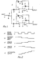
- Figure 1 the various switches of the switched capacitors are shown in one of their two switching states; all of the switches are operated in synchronism by means not shown. The switches are controlled and are implemented by CMOS devices as is well known in the art.
- the switched-capacitor stage produces differential output signals at output terminals 1 and 2 from a single-ended input signal at an input 3.
- the stage provides two signal paths 4 and 5 from the input 3 to the output terminals 1 and 2 respectively. Except for the timing of the switch operations, the two signal paths are identical.
- Each signal path includes a differential amplifier 7, having an output connected to the respective output terminal 1 or 2, a non-inverting input connected to circuit ground, and an inverting input; an unswitched integrating capacitor 8 connected between the inverting input and the output of the amplifier; a through-switched negative feedback capacitor 9 connected via a switch 10 to the output of the amplifier and via a switch 11 to the inverting input of the amplifier; a further switched-capacitor 12 having one terminal connected to the junction between the capacitor 9 and the switch 11, and hence connected to the inverting input of the amplifier via the switch 11; and a further switch 13 connecting the other terminal of the capacitor 12 to the input 3.
- a single switch 13 serves commonly for the two signal paths 4 and 5, but separate switches could be provided if desired.
- the switches 10, 11, and 13 are all operated in synchronism with one another, for example at a switching frequency of 125kHz for handling voice-frequency signals at frequencies up to 3.5kHz.
- the switches 10 and 11 in the signal path 5 are operated with the opposite phase to the switch 13 and to the switches 10 and 11 in the signal path 4.
- the capacitor 9 is through-switched via the switches 10 and 11 and the capacitor 12 is through-switched via the switches 13 and 11
- the capacitor 9 is through-switched via the switches 10 and 11 but the capacitor 12 is diagonally-switched via the switches 13 and 11.
- the input signal is applied to the inverting input of the amplifier 7 in the signal path 5 inverted and delayed by half of one period of the switching frequency.
- the inversion results in the production of the differential output signals at the output terminals 1 and 2.
- the delay is advantageous in providing an interpolation effect as described below with reference to Figure 2.
- Figure 2 illustrates signals which may occur during three cycles of a digital switch control waveform shown at Figure 2(a), the switches 10, 11 and 13 in Figure 1 being in the states shown in Figure 1 when the digital switch control waveform is a logic 1 level.
- Figure 2(b) shows a switched analog input signal which is assumed to be applied to the input 3 from preceding switched-capacitor circuitry. This input as shown in Figure 2(b) is of decreasing magnitude, each magnitude level remaining constant for the duration of one period of the switch control waveform.
- the resultant switched analog outputs at the terminals 1 and 2 are shown in Figures 2(c) and 2(d) respectively, the output at the terminal 2 being inverted and delayed by half a period in relation to that at the terminal 1 due to the diagonally-switched capacitor 12 in the signal path 5, and the related switching state timing.
- the resultant differential output signal, shown in Figure 2(e) has steps occurring at twice the switch control frequency at a relative magnitude only half that of the input and individual output signals. This interpolation effect, providing doubled step frequency and halved relative step magnitude, considerably facilitates filtering and smoothing of the differential output signal.
- each of the capacitors may, for example, have a nominal capacitance of 2pF, the bottom plate of each capacitor being represented by a curved line in Figure 1.
- each output of the stage in Figure 1 may be additionally provided with a power buffer stage and an output protection device of known form.
Landscapes
- Engineering & Computer Science (AREA)
- Power Engineering (AREA)
- Amplifiers (AREA)
- Filters That Use Time-Delay Elements (AREA)
Abstract
Description
- This invention relates to a switched-capacitor stage for producing differential output signals from a single-ended input signal.
- It is generally known to produce differential output signals from a single-ended input signal using two buffer amplifiers, one of which is inverting and the other non-inverting, or using two similar buffer amplifiers with an inverting amplifier connected from the input or output of one of them to the input of the other. These arrangements have the disadvantage of having different output characteristics for the different buffers and/or different signal delays through the different signal paths.
- Accordingly, an object of this invention is to provide a new arrangement for producing differential output signals from a single-ended input signal using switched-capacitor techniques. Such an arrangement is particularly useful where preceding circuitry also uses switched-capacitor techniques, but the invention is not limited in this respect.
- According to one aspect the invention provides a switched-capacitor stage having a single-ended input and a differential output, the stage comprising a first through-switched capacitor coupled between said input and a first differential output terminal, and a second diagonally-switched capacitor coupled between said input and a second differential output terminal.
- Preferably the stage includes first and second amplifiers via which the first and second capacitors respectively are coupled to the first and second output terminals respectively, two unswitched capacitors each coupled between an output and an inverting input of a respective one of the amplifiers, and first and second through-switched negative feedback capacitors coupled to the first and second amplifiers respectively.
- Expediently said first through-switched capacitor and the first through-switched negative feedback capacitor comprise common switching means coupled between said capacitors and the inverting input of the first amplifier, and said second diagonally-switched capacitor and the second through-switched negative feedback capacitor comprise common switching means coupled between said capacitors and the inverting input of the second amplifier.
- The stage conveniently comprises switching means, which is common to said through-switched capacitor and said second diagonally-switched capacitor, coupled between said input and each of said first and second capacitors.
- According to another aspect the invention provides a switched-capacitor stage comprising first and second signal paths from a single-ended input to a respective one of two differential output terminals, each signal path comprising an amplifier having an inverting input and an output coupled to the respective output terminal, an unswitched capacitor coupled between the inverting input and the output of the amplifier, a feedback capacitor and first and second switching means for selectively and simultaneously connecting the terminals of the feedback capacitor either to the output and inverting input respectively of the amplifier or to a reference potential, a further capacitor having one terminal connected to the junction between the feedback capacitor and the second switching means, and third switching means for connecting the other terminal of the further capacitor selectively to either the input or the reference potential synchronously with the first and second switching means, the operations of the first and second switching means relative to those of the third switching means of the two signal paths being oppositely phased whereby the further capacitor of the first signal path is through-switched and the further capacitor of the second signal path is diagonally-switched to produce differential output signals from a single-ended input signal.
- Thus the invention uses a through-switched capacitor and a diagonally-switched capacitor in respective signal paths to provide differential outputs from a single-ended input. As explained below, this arrangement also effects an interpolation of the differential output signal, which is advantageous.
- The invention will be further understood from the following description with reference to the accompanying drawings, in which:
- Figure 1 schematically illustrates a switched-capacitor stage according to a preferred embodiment of the invention; and
- Figure 2 is a signal diagram illustrating the interpolating effect of the stage.
- As used herein, the term "unswitched capacitor" means a capacitor that is permanently connected in the circuit; the term "through-switched capacitor" means a switched-capacitor whose two terminals are simultaneously grounded, or connected to a reference potential, during one of two switching states; and the term "diagonally-switched capacitor" means a switched-capacitor whose terminals are alternately grounded during successive ones of two switching states. In Figure 1 the various switches of the switched capacitors are shown in one of their two switching states; all of the switches are operated in synchronism by means not shown. The switches are controlled and are implemented by CMOS devices as is well known in the art.
- Referring to Figure 1, the switched-capacitor stage produces differential output signals at
output terminals signal paths 4 and 5 from the input 3 to theoutput terminals respective output terminal unswitched integrating capacitor 8 connected between the inverting input and the output of the amplifier; a through-switchednegative feedback capacitor 9 connected via aswitch 10 to the output of the amplifier and via aswitch 11 to the inverting input of the amplifier; a further switched-capacitor 12 having one terminal connected to the junction between thecapacitor 9 and theswitch 11, and hence connected to the inverting input of the amplifier via theswitch 11; and afurther switch 13 connecting the other terminal of thecapacitor 12 to the input 3. Asingle switch 13 serves commonly for the twosignal paths 4 and 5, but separate switches could be provided if desired. - The
switches switches switch 13 and to theswitches signal path 4. In consequence, in thesignal path 4 thecapacitor 9 is through-switched via theswitches capacitor 12 is through-switched via theswitches capacitor 9 is through-switched via theswitches capacitor 12 is diagonally-switched via theswitches - As a result of the diagonal switching of the
capacitor 12 in the signal path 5, and the phasing of theswitches switch 13, the input signal is applied to the inverting input of the amplifier 7 in the signal path 5 inverted and delayed by half of one period of the switching frequency. The inversion results in the production of the differential output signals at theoutput terminals - Figure 2 illustrates signals which may occur during three cycles of a digital switch control waveform shown at Figure 2(a), the
switches logic 1 level. Figure 2(b) shows a switched analog input signal which is assumed to be applied to the input 3 from preceding switched-capacitor circuitry. This input as shown in Figure 2(b) is of decreasing magnitude, each magnitude level remaining constant for the duration of one period of the switch control waveform. The resultant switched analog outputs at theterminals terminal 2 being inverted and delayed by half a period in relation to that at theterminal 1 due to the diagonally-switchedcapacitor 12 in the signal path 5, and the related switching state timing. The resultant differential output signal, shown in Figure 2(e), has steps occurring at twice the switch control frequency at a relative magnitude only half that of the input and individual output signals. This interpolation effect, providing doubled step frequency and halved relative step magnitude, considerably facilitates filtering and smoothing of the differential output signal. - As will be appreciated by those skilled in the art, the switched-capacitor stage illustrated in Figure 1 can be implemented, together with other switched-capacitor circuitry if desired, in a single integrated circuit, for example using a CMOS double polysilicon process. In such an arrangement each of the capacitors may, for example, have a nominal capacitance of 2pF, the bottom plate of each capacitor being represented by a curved line in Figure 1. In order to facilitate use of such an arrangement in, for example, a telephone repeater for voice frequency channels, each output of the stage in Figure 1 may be additionally provided with a power buffer stage and an output protection device of known form.
- The invention is not limited to the particular embodiment described, and numerous modifications, variations, and adaptations may be made thereto without departing from the scope of the invention as defined in the claims.
Claims (6)
Applications Claiming Priority (2)
| Application Number | Priority Date | Filing Date | Title |
|---|---|---|---|
| CA409631 | 1982-08-18 | ||
| CA000409631A CA1173522A (en) | 1982-08-18 | 1982-08-18 | Switched capacitor stage with differential output |
Publications (3)
| Publication Number | Publication Date |
|---|---|
| EP0103410A2 true EP0103410A2 (en) | 1984-03-21 |
| EP0103410A3 EP0103410A3 (en) | 1986-02-12 |
| EP0103410B1 EP0103410B1 (en) | 1989-11-02 |
Family
ID=4123430
Family Applications (1)
| Application Number | Title | Priority Date | Filing Date |
|---|---|---|---|
| EP19830304669 Expired EP0103410B1 (en) | 1982-08-18 | 1983-08-12 | Switched-capacitor stage with differential output |
Country Status (3)
| Country | Link |
|---|---|
| EP (1) | EP0103410B1 (en) |
| CA (1) | CA1173522A (en) |
| DE (1) | DE3380801D1 (en) |
Cited By (1)
| Publication number | Priority date | Publication date | Assignee | Title |
|---|---|---|---|---|
| FR2631181A1 (en) * | 1988-05-03 | 1989-11-10 | France Etat | INTERFACE CIRCUIT FOR SWITCHED CAPACITY CIRCUIT |
Family Cites Families (1)
| Publication number | Priority date | Publication date | Assignee | Title |
|---|---|---|---|---|
| CH625373A5 (en) * | 1978-12-18 | 1981-09-15 | Centre Electron Horloger |
-
1982
- 1982-08-18 CA CA000409631A patent/CA1173522A/en not_active Expired
-
1983
- 1983-08-12 DE DE8383304669T patent/DE3380801D1/en not_active Expired
- 1983-08-12 EP EP19830304669 patent/EP0103410B1/en not_active Expired
Cited By (1)
| Publication number | Priority date | Publication date | Assignee | Title |
|---|---|---|---|---|
| FR2631181A1 (en) * | 1988-05-03 | 1989-11-10 | France Etat | INTERFACE CIRCUIT FOR SWITCHED CAPACITY CIRCUIT |
Also Published As
| Publication number | Publication date |
|---|---|
| CA1173522A (en) | 1984-08-28 |
| EP0103410A3 (en) | 1986-02-12 |
| EP0103410B1 (en) | 1989-11-02 |
| DE3380801D1 (en) | 1989-12-07 |
Similar Documents
| Publication | Publication Date | Title |
|---|---|---|
| US4453130A (en) | Switched-capacitor stage with differential output | |
| US4970703A (en) | Switched capacitor waveform processing circuit | |
| US4430629A (en) | Electrical filter circuit operated with a definite sampling and clock frequency fT which consists of CTD elements | |
| US4651034A (en) | Analog input circuit with combination sample and hold and filter | |
| JPS6329849B2 (en) | ||
| EP0396123A3 (en) | Parallel connection multi-stage band-pass filter | |
| US5081372A (en) | Sample-and-hold device | |
| IE810195L (en) | Electronic hybrid circuit | |
| EP0122663A3 (en) | Method and system for improving speaker performance | |
| US4453143A (en) | Switched-capacitor variable equalizer | |
| EP0379202A3 (en) | Phase inverter and push-pull amplifier using the same | |
| US4306197A (en) | Switched-capacitor elliptic filter | |
| US4218665A (en) | Band-pass filter | |
| CA1173522A (en) | Switched capacitor stage with differential output | |
| JP3465951B2 (en) | Inverting delay circuit | |
| US3999137A (en) | Low pass active filter apparatus | |
| US4745594A (en) | Offset-compensated switched-capacitor filter for TDM multichannel analog signals | |
| KR870005547A (en) | Demetrical Circuit | |
| JPS59167109A (en) | Two-terminal impedance circuit | |
| JP2925333B2 (en) | Push button signal generation circuit | |
| KR970004289A (en) | Voltage Gain Amplifier Converts Single Input to Differential Output | |
| JPS57162185A (en) | Sample holding circuit | |
| JPS5680952A (en) | Subscriber monitoring circuit | |
| SU517986A1 (en) | Broadband amplifier | |
| JPS6468004A (en) | Rat race mixer |
Legal Events
| Date | Code | Title | Description |
|---|---|---|---|
| PUAI | Public reference made under article 153(3) epc to a published international application that has entered the european phase |
Free format text: ORIGINAL CODE: 0009012 |
|
| AK | Designated contracting states |
Designated state(s): DE FR GB NL SE |
|
| PUAL | Search report despatched |
Free format text: ORIGINAL CODE: 0009013 |
|
| RHK1 | Main classification (correction) |
Ipc: H03F 3/00 |
|
| AK | Designated contracting states |
Designated state(s): DE FR GB NL SE |
|
| 17P | Request for examination filed |
Effective date: 19860605 |
|
| 17Q | First examination report despatched |
Effective date: 19881005 |
|
| GRAA | (expected) grant |
Free format text: ORIGINAL CODE: 0009210 |
|
| AK | Designated contracting states |
Kind code of ref document: B1 Designated state(s): DE FR GB NL SE |
|
| REF | Corresponds to: |
Ref document number: 3380801 Country of ref document: DE Date of ref document: 19891207 |
|
| ET | Fr: translation filed | ||
| PLBE | No opposition filed within time limit |
Free format text: ORIGINAL CODE: 0009261 |
|
| 26N | No opposition filed | ||
| PGFP | Annual fee paid to national office [announced via postgrant information from national office to epo] |
Ref country code: SE Payment date: 19920817 Year of fee payment: 10 |
|
| PGFP | Annual fee paid to national office [announced via postgrant information from national office to epo] |
Ref country code: NL Payment date: 19920831 Year of fee payment: 10 |
|
| PG25 | Lapsed in a contracting state [announced via postgrant information from national office to epo] |
Ref country code: SE Effective date: 19930813 |
|
| PG25 | Lapsed in a contracting state [announced via postgrant information from national office to epo] |
Ref country code: NL Effective date: 19940301 |
|
| NLV4 | Nl: lapsed or anulled due to non-payment of the annual fee | ||
| PGFP | Annual fee paid to national office [announced via postgrant information from national office to epo] |
Ref country code: DE Payment date: 19940816 Year of fee payment: 12 |
|
| EUG | Se: european patent has lapsed |
Ref document number: 83304669.1 Effective date: 19940310 |
|
| PG25 | Lapsed in a contracting state [announced via postgrant information from national office to epo] |
Ref country code: DE Effective date: 19960501 |
|
| PGFP | Annual fee paid to national office [announced via postgrant information from national office to epo] |
Ref country code: GB Payment date: 20010808 Year of fee payment: 19 |
|
| PGFP | Annual fee paid to national office [announced via postgrant information from national office to epo] |
Ref country code: FR Payment date: 20010810 Year of fee payment: 19 |
|
| REG | Reference to a national code |
Ref country code: GB Ref legal event code: IF02 |
|
| PG25 | Lapsed in a contracting state [announced via postgrant information from national office to epo] |
Ref country code: GB Free format text: LAPSE BECAUSE OF NON-PAYMENT OF DUE FEES Effective date: 20020812 |
|
| GBPC | Gb: european patent ceased through non-payment of renewal fee |
Effective date: 20020812 |
|
| PG25 | Lapsed in a contracting state [announced via postgrant information from national office to epo] |
Ref country code: FR Free format text: LAPSE BECAUSE OF NON-PAYMENT OF DUE FEES Effective date: 20030430 |
|
| REG | Reference to a national code |
Ref country code: FR Ref legal event code: ST |