EP0101571A1 - Differential voltage amplifier - Google Patents
Differential voltage amplifier Download PDFInfo
- Publication number
- EP0101571A1 EP0101571A1 EP83107285A EP83107285A EP0101571A1 EP 0101571 A1 EP0101571 A1 EP 0101571A1 EP 83107285 A EP83107285 A EP 83107285A EP 83107285 A EP83107285 A EP 83107285A EP 0101571 A1 EP0101571 A1 EP 0101571A1
- Authority
- EP
- European Patent Office
- Prior art keywords
- signal
- mode
- voltage
- capacitive coupling
- amplifying
- Prior art date
- Legal status (The legal status is an assumption and is not a legal conclusion. Google has not performed a legal analysis and makes no representation as to the accuracy of the status listed.)
- Granted
Links
Images


Classifications
-
- H—ELECTRICITY
- H03—ELECTRONIC CIRCUITRY
- H03K—PULSE TECHNIQUE
- H03K5/00—Manipulating of pulses not covered by one of the other main groups of this subclass
- H03K5/22—Circuits having more than one input and one output for comparing pulses or pulse trains with each other according to input signal characteristics, e.g. slope, integral
- H03K5/24—Circuits having more than one input and one output for comparing pulses or pulse trains with each other according to input signal characteristics, e.g. slope, integral the characteristic being amplitude
- H03K5/2472—Circuits having more than one input and one output for comparing pulses or pulse trains with each other according to input signal characteristics, e.g. slope, integral the characteristic being amplitude using field effect transistors
- H03K5/249—Circuits having more than one input and one output for comparing pulses or pulse trains with each other according to input signal characteristics, e.g. slope, integral the characteristic being amplitude using field effect transistors using clock signals
-
- H—ELECTRICITY
- H03—ELECTRONIC CIRCUITRY
- H03M—CODING; DECODING; CODE CONVERSION IN GENERAL
- H03M1/00—Analogue/digital conversion; Digital/analogue conversion
- H03M1/12—Analogue/digital converters
- H03M1/34—Analogue value compared with reference values
- H03M1/36—Analogue value compared with reference values simultaneously only, i.e. parallel type
- H03M1/361—Analogue value compared with reference values simultaneously only, i.e. parallel type having a separate comparator and reference value for each quantisation level, i.e. full flash converter type
Abstract
Description
- This invention relates to a difference voltage amplifier circuit for amplifying a differential voltage between an input signal voltage and a reference voltage.
- By convention, a general parallel A/D (analog to digital) converter is provided with a plurality of differential amplifiers each composed of a bipolar transistor. This type of parallel A/D converter will be described referring to Fig. 1. In Fig. 1,
reference numeral 1 designates a voltage divider composed of resistors. Positive and negative reference voltages +Vref and -Vref are applied to the terminals of thevoltage divider 1. The divided voltages derived from the interconnection points of the resistors connected in series are input, as reference voltages Vrefl - Vrefn, to the input terminals of the differential amplifiers 21 - 2n composed of bipolar transistors, those input terminals each being one of the input terminals of each of the differential amplifiers 21 - 2n. An input signal voltage Vin is applied to the other input terminals of the differential amplifiers 21 - 2n, where the input signal voltage Vin is compared with the reference voltages Vrefl - Vrefn. The differential amplifiers 21 - 2n respectively amplify differences between the input signal voltage Vin and the reference voltages Vrefl - Vrefn. The output signal voltages Vol - Von are input to anencoder 3 where these are encoded. Then, the encoded signal is applied through anoutput resister 4 to abuffer 5, which in turn produces digital signals D and D. - In the example mentioned above, the differential amplifiers 21 - 2n are composed of bipolar transistors, even several tens of MHz can be sampled, i.e., the circuit is operable at high speed.
- With such an arrangement, the offset voltages of the differential amplifiers 21 - 2n differ depending on the magnitudes of the reference voltages Vrefl, Vref2, ..., Vrefn to the differential amplifiers 21 - 2n. This fact implies that the circuit has a problem of linearity. Further, differential amplifiers using the bipolar transistors require great power dissipation.
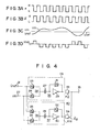
- Another known approach to solving such a problem is an A/D converter using the chopper type comparator, as shown in Fig. 2. In the chopper type comparator, the
first input terminal 6 is applied with a reference voltage Vref (Fig. 3C). Thesecond input terminal 7 is applied with an input signal voltage Vin (Fig. 3C) to be compared with the reference voltage Vref. The first andsecond input terminals capacitor 10, through first and second switches 8 and 9. The first and second switches 8 and 9 are analog switches made of FETs (field effect transistors), for example. These switches are on-off controlled by a clock signal ¢ (Fig. 3A) and its inverted signal $ (Fig. 3B). The reference voltage Vref and the input signal voltage Vin are applied to the first terminal of thecapacitor 10, through the first and second switches 8 and 9. A second terminal or output electrode of thecapacitor 10 is connected to the input terminal of an inverting amplifier 11 composed of a MOS transistor. Athird switch 12 made up of an FET analog switch, for example, which is on-off controlled by the clock signal ¢, is provided between the input and output terminals of the inverting amplifier 11. The output signal Vout (Fig. 3D) of the inverting amplifier 11 is taken out through anoutput terminal 13. - With such an arrangement, during the "H" level period of the clock signal (Fig. 3A), the first switch 8 and the
third switch 12 are turned on, while the second switch 9 is turned off. Therefore, the input electrode of thecapacitor 10 is applied with the reference voltage Vref (Fig. 3C). The input and output terminals of the inverting amplifier 11 are shortcircuited so that the input voltage of the inverting amplifier 11 may be made a threshold voltage VTH of the inverting amplifier 11, i.e., an operating point voltage as a reference voltage for the circuit operation. During the "H" level period of the clock t (Fig. 3B), the first andthird switches 8 and 12 are turned off, while the second switch 9 is turned on. Accordingly, the input electrode of thecapacitor 10 is applied with the input signal voltage Vin. - Then, the input voltage, i.e., the threshold voltage VTH, to the inverting amplifier 11 changes by a difference (Vin - Vref). A change of the input voltage is multiplied by an amplification factor of the inverting amplifier 11 and is taken out as a circuit output signal Vout (Fig. 3D) from the
output terminal 13. As described above, in this comparator of Fig. 2, it is possible to obtain an output signal Vout (Fig. 3D) composed of a train of pulses in synchronism with the clock signal by setting the reference voltage Vref at a proper value with respect to the input signal voltage Vin (Fig. 3C). In this way, the above-mentioned circuit arrangement alternately repeats an autozeroed mode in which the circuit operating point is set up by shorting the input and the output of the inverting amplifier 11, and a signal amplifying mode for inputting tQ the inverting amplifier 11 a difference between the input signal voltage Vin and the reference voltage Vref and amplifying the same. Through this operation, an output signal voltage Vout shown in Fig. 3D is obtained. - The comparator as mentioned above has a low power dissipation since the inverting amplifier 11 is composed of the MOS transistor. However, since this chopper type of comparator operates as a sampling system, it will be understood from the sampling theory that the comparator fails to correctly sample the input signal voltage Vin when the frequency of the input signal voltage Vin is higher than 1/2 the frequency of the clock signal ¢. To perform high speed sampling, the influence of both a stray capacitance and an ON resistance, becomes distinctive because the ON duration of the switch is short in the high speed sampling operation. The stray capacitance and the ON resistance cause a signal transfer delay, a gain loss, etc. Further, a stray capacitance, which appears between the signal input terminal and the signal output terminal, and the control terminal of the switch for receiving the clock ¢, cause a feedthrough of clock pulses into the input signal to produce whisker- like pulses at the level-changing of the clock pulse. This pulse signal renders the output signal unstable. Following this unstable state, a relatively long time is required until the circuit operation settles down to be stable. Because of this, the high speed circuit operation is damaged from a dynamic viewpoint of the circuit, and the output signal of the circuit is set off from a static viewpoint.
- Accordingly, an object of the present invention is to provide a differential voltage amplifying circuit which can perform a successive comparison of a high frequency input signal voltage with a reference voltage and requires low power consumption and is free from the adverse influence from stray capacitance.
- Another object of the present invention is to provide an integrated circuit for analog-to-digital conversion with such a differential voltage amplifying circuit incorporated thereinto.
- According to the invention, there is provided a differential voltage amplifier comprising:
- first and second capacitive coupling type amplifying means in each of which an autozeroed mode period for setting an operating point and a signal amplifying mode period for amplifying an input voltage are alternately set up, and the autozeroed mode periods in said first and second amplifying means are shifted from each other;
- first and second mode select means for alternately setting up the autozeroed mode and the signal amplifying mode in said first and second capacitive coupling type amplifying means;
- first and second signal selecting means provided corresponding to said first and second capacitive coupling type amplifying means, said first and second signal selecting means alternately selecting a reference voltage and an input signal voltage to apply the selected signal to said first and second capacitive coupling type amplifying means, said first and second signal selecting means further selecting the reference voltage corresponding to the autozeroed mode periods of said first and second capacitive coupling type amplifying means and the input signal voltage corresponding to the signal amplifying mode periods; and
- means for selecting the amplified signal output from said first and second capacitive coupling type amplifying means when said first and second capacitive coupling type amplifying means are in the signal amplifying mode.
- According to the invention, there is further provided an integrated circuit for A/D conversion comprising:
- a plurality of differential voltage amplifiers whose first input terminals are applied with an input signal voltage and whose second input terminals are applied with different reference voltages, each of said differential voltage amplifiers including;
- first and second capacitive coupling type amplifying means each of which are alternately set in an autozeroed mode period for setting an operating point and a signal amplifying mode period for amplifying an input voltage, the periods of the autozeroed modes in said first and second amplifying means being shifted from each other;
- first and second mode selecting means for alternately setting up the autozeroed mode and the signal amplifying mode in said first and second capacitive coupling type amplifying means;
- first and second signal selecting means provided corresponding to said first and second capacitive coupling type amplifying means, said first and second signal selecting means alternately selecting a reference voltage and an input signal voltage to apply the selected signal to said first and second capacitive coupling type amplifying means, said first and second signal selecting means further selecting the reference voltage corresponding to the autozeroed mode periods of said first and second capacitive coupling type amplifying means and the input signal voltage corresponding to the signal amplifying mode periods; and
- means for selecting the amplified signal output from said first and second capacitive coupling type amplifying means when said first and second capacitive coupling type amplifying means are in the signal amplifying mode.
- This invention can be more fully understood from the following detailed description when taken in conjunction with the accompanying drawings, in which:
- Fig. 1 is a circuit diagram of an example of a prior parallel A/D converter;
- Fig. 2 is a circuit diagram of an example of a prior chopper type comparator;
- Figs. 3A to 3D show timing charts of signals at key portions in the comparator of Fig. 2;
- Fig. 4 shows a circuit arrangement of an embodiment of a differential voltage amplifier circuit according to the present invention;
- Figs. 5A to 5J show timing charts of signals at key portions of the circuit of Fig. 4;
- Fig. 6 shows a schematic circuit diagram of an integrated circuit for A/D conversion, which.is another embodiment of the present invention and has the amplifying circuit shown in Fig. 4;
- Figs. 7 to 9 show other circuit arrangements of the differential voltage amplifier shown in Fig. 4;
- Figs. 10 to 13 show circuit diagrams of some types of inverting amplifiers assembled into the differential voltage amplifier of Fig. 4; and
- Figs. 14 through 17 show circuit diagrams of some types of switches each assembled into the differential voltage amplifier of Fig. 4.
- Reference is made to Fig. 4 illustrating in block form an embodiment of a differential voltage amplifier according to this invention. The differential voltage amplifier is comprised of
chopper type comparators 101 and 102, and seventh andeighth switches chopper type comparators 101 and 102. The firstchopper type comparator 101 includes afirst switch 23, asecond switch 24 andfifth switch 31, afirst capacitor 27, and afirst inverting amplifier 29. The second chopper type comparator 102 likewise includes athird switch 25, afourth switch 26 and asixth switch 32, asecond capacitor 28, and asecond inverting amplifier 30. Those switches 23 to 26 and 31 to 36 are FET analog switches, for example.Reference numeral first input terminal 21 is connected via thefirst switch 23 to the input electrode of thefirst capacitor 27 and via thethird switch 25 to the input electrode of thesecond capacitor 28. Thesecond input terminal 22 is connected via thesecond switch 24 to the input electrode of thefirst capacitor 27, and via thefourth switch 26 to the input electrode of thesecond capacitor 28. The output electrodes of thefirst capacitor 27 and thesecond capacitor 28 are respectively connected to the input terminals of thefirst inverting amplifier 29 and second invertingamplifier 30 made up of MOS transistors. Thefifth switch 31 andsixth switch 32 are respectively inserted between the input and output terminals of thefirst inverting amplifier 29 and second invertingamplifier 30. The output terminals of thefirst inverting amplifier 29 and second invertingamplifier 30 are connected to theoutput terminal 35 through seventh andeighth switches - The
first capacitor 27 and thefirst inverting amplifier 29 make up a first capacitivecoupling amplifier circuit 36. Thesecond capacitor 28 and thesecond inverting amplifier 30 compose a second capacitivecoupling amplifier circuit 37. - The
fifth switch 31 serves as a first mode select means for alternately setting up an autozeroed mode to provide an operating point as a reference for the circuit operation and a signal amplifying mode for amplifying the input voltage. Thesixth switch 32 serves as a second mode select means for alternately setting up an autozeroed mode to provide an operating point as a reference for the circuit operation and a signal amplifying mode for amplifying the input voltage. The first andsecond switches coupling amplifying circuit 36. The first selectingmeans 38 selects a reference signal voltage Vref during the autozeroed mode period of the first amplifying circuit, and selects the input signal voltage Vin during the signal amplifying mode period. The third andfourth switches coupling amplifying circuit 37. The second signal selecting means selects the reference signal voltage Vref corresponding to the autozeroed mode period of the second amplifying circuit, and selects the input signal voltage Vin corresponding to the_ signal amplifying period. The seventh andeighth switches fifth switches second switch 24 is controlled by the inverted clock signalφ 1 (Fig. 5B). The third andsixth switches fourth switch 26 is controlled by the inverted clock T2 (Fig. 5D). Theseventh switch 33 is controlled by the clock t12 (Fig. 51). - The operation of the differential voltage amplifier shown in Fig. 4 will be described referring to signal timing charts shown in Figs. 5A to 5J. Each of these switches is turned on when the control clock signal is "H" in logical level and is turned off when it is "L" in logical level.
- When the clock φ 1 (Fig. 5A) is "H" (e.g., duration t3 - t4), the first and
fifth switches comparator 101 are turned on, and thesecond switch 24 is turned off. When thefirst switch 23 is turned on, the reference voltage Vref (Fig. 5E) is selected as the input voltage to the firstcapacitive coupling amplifier 36. Upon turning on thefifth switch 31, the first capacitivecoupling amplifier circuit 36 is set in the autozeroed mode for providing the operating point potential as a reference of the circuit operation. During the "H" level period of theclock φ 1, the threshold voltage VTH as the operation point voltage is set up at the input terminal of thefirst inverting amplifier 29. The clock φ 2 (Fig. 5C), contains the "H" level period of theclock φ 1, and keeps "L" level during a proper period (e.g., from time t1 to time t6), including the periods preceding and succeeding the "H" level period. During the "L" level of the clock φ 2, the second andthird comparators fourth switch 26 i.s turned on. When thefourth switch 26 is turned on, the input signal voltage Vin (Fig. 5E) is selected as the input signal voltage to the second capacitivecoupling amplifier circuit 37. When thesixth switch 32 is turned off, the second capacitivecoupling amplifier circuit 37 is set in the signal amplifying mode. During the "H" level period of the clock φ 2, i.e., the autozeroed mode period of the second capacitivecoupling amplifier circuit 37, the third switches is turned on and thefourth switch 26 is turned off. The reference voltage Vref is input to the second capacitivecoupling amplifier circuit 37. During the signal amplifying mode period when the clock φ 2 is "L" level, thesecond capacitor 28 applies a difference voltage between the reference voltage Vref and the input signal voltage Vin to the second invertingamlifier 30. Thesecond inverting amplifier 30 amplifies this differential voltage. The clock φ 12 (Fig. 5H) contains the "H" level period of theclock φ 1 and is at "L" level during a period including the periods (time t2 to time t6) preceding and succeeding the "H" level period. Accordingly, theseventh switch 33 is off and theeighth switch 34 is on, so that the amplified signal Vo2 (Fig. 5G) output from the second capacitivecoupling amplifier circuit 37 is applied as the circuit output Vout (Fig. 5J) to theoutput terminal 35 of the differential voltage amplifier. It is necessary that the "L" level period of the clock $2 be equal to or shorter than the" "L" level period of the clock §2. In this embodiment, the former is shorter than the latter. - At time t4, when the clock φ1 is "L", the first and
fifth switches chopper type comparator 101 are off and thesecond switch 24 is ON. Accordingly, the first capacitivecoupling amplifier circuit 36 is set in the signal ammplifying mode and is supplied with the input signal voltage Vin. As in the previous case, thefirst inverting amplifier 29 amplifies the difference voltage between the reference voltage Vref and the input signal voltage Vin, and produces an amplified signal Vol (Fig. 5F). For a short while from the start of the signal amplifying period, because of a signal transfer delay or the like caused by the feedthrough of the clock signal through the stray capacitor and the ON resistance of the switches, the output signal of thecapacitor 101, i.e., the output signal Vol (Fig. 5F) from thefirst inverting amplifier 29, varies as indicated by a broken line in Fig. 5F. To avoid the production of this varying output signal Vol, theclock φ 12 does not go high ("H" level) when theclock φ 1 goes low ("L" level), but goes high following the period T after theclock φ 1 has become "L". This period T is equal to the time period from an instant that the clock $1 goes low at least until it settles down to a stable state. Accordingly, until the end of the period tl, the output signal Vol of the first capacitive coupling amplifier circuit, 36 is not produced as the output signal Vout of the differential voltage amplifier, but the output amplified signal from the second capacitivecoupling amplifier circuit 37 is produced continuously. After the end of the period T, at time t5, the output signal Vol from the first capacitivecoupling amplifier circuit 36 is produced as the circuit output signal. - At time t6, after at least the period T since time t4, the clock 2 goes high and the third and the sixth switches'25 and 32 of the chopper type comparator 102 are turned on, and the
fourth switch 26 is turned off. The second capacitivecoupling amplifier circuit 37 is set in the autozeroed mode and the reference voltage Vref is selected as the input signal voltage of the second capacitivecoupling amplifier circuit 37. The operating point voltage, i.e., the threshold voltage VTH, of thesecond inverting amplifier 30 in the second capacitivecoupling amplifier circuit 37 is set in the autozeroed mode. The "L" level period of theclock φ 1 contains the "H" level period of the clock φ 2 (the period from time t4 to t9) and extends to the period preceding and succeeding this "L" level period. During this period, the first capacitivecoupling amplifier circuit 36 produces the difference voltage signal Vol between the reference voltage Vref and the input signal voltage Vin. When the clock t2 goes low at time t7, the third andsixth switches fourth switch 26 is turned on. As a result, the second capacitivecoupling amplifier circuit 37 is set in the signal amplifying mode and the input signal voltage Vin is selected as the input signal voltage to the second capacitivecoupling amplifier circuit 37. Therefore, the second capacitivecoupling amplifier circuit 37 produces the difference voltage signal Vo2 (Fig. 5G). During the transition period in which theclock φ 1 goes low, the transient phenomenon occurs also when the clock t2 goes low, so that the amplified output Vo2 from the second capacitivecoupling amplifier circuit 37 is unstable. To avoid the outputting of this unstable signal from the differential voltage amplifier, theclock φ 12 goes low at time t8, which is time period T after the clock φ 2 goes low. During the time period T from time T7 to T8, the output signal voltage Vol from the first capacitivecoupling amplifier circuit 36 is taken out as the circuit output voltage Vout of the differential voltage amplifier, through theoutput terminal 35. At time t8, theclock φ 12 goes low and then the output signal voltage Vo2 from the second capacitivecoupling amplifier circuit 37 is selected as the output signal voltage Vout and output through theoutput terminal 35. At time t9 after a period of at least the time perid T since time t7, the clock 1 goes low and the differential voltage amplifier repeats the above-mentioned operation subsequently. - As seen from the 'foregoing, the differential voltage amplifier of this embodiment contains the first and second capacitive
coupling amplifier circuits amplifiers amplifiers - Fig. 6 shows a block diagram of an integrated circuit for analog-to-digital conversion using the differential voltage amplifier shown in Fig. 4, which is another embodiment of the present invention. In Fig. 6, reference numerals 2011 - 201n designate differential voltage amplifiers, as illustrated in block form in Fig. 4. This instance uses 64 differential voltage amplifiers. The input signal voltage Vin is externally applied to the input terminal through a first terminal Tl of the integrated circuit. In this integrated circuit using 64 differential voltage amplifiers 2011 - 201n, a
voltage dividing circuit 202 having a series circuit of 65 resistors Rl - R65 is inserted between a positive reference voltage terminal T2 and a negative reference voltage terminal T3 of the integrated circuit. The interjunctions between the adjacent resistors Rl and R2, R2 and R3, ... are connected to the first input terminals of the differential voltage amplifiers 2011 - 201n, respectively. The divided voltages at these interjunctions are respectively connected to the corresponding second input terminals of the differential voltage amplifiers 2011 - 201n, so that the divided voltages at the interjunctions are applied as the reference voltages Vrefl - Vrefn to the corresponding second input terminals of thedifferential voltage amplifiers 2011, ..., 201n. - The comparing outputs of the differential voltage amplifiers 2011 - 201n are input to the
encoder circuit 203. Theencoder circuit 203 encodes the comparing output signal into a 6-bit signal. Theencoder circuit 203 has the following compositions, although not shown: a plurality of comparing circuits which are respectively provided for the differential voltage amplifiers 2011 - 201n and compares the amplified signals with the threshold voltages previously set to convert those amplified signals into a digital signal; a plurality of latch circuits for latching digital signals output from the comparing circuits in response to a latch signal $L; an encoder section for converting the digital signals into a binary signal of e.g., 6 bits; an error-detecting circuit for detecting an error; an overflow detecting circuit for detecting an overflow. The 6 bit signals from theencoder circuit 203 are input to latch circuits 2041 - 2046 through their D terminals in response to a latch signal FL and latched in those latch circuits. - The bit signals latched in the latch circuits 2041 - 2046 are output through the Q terminal thereof. The bit signals are transferred to buffers 205i - 2056 with gate functions, respectively. The bit signals input are taken out from output terminals T5 - T10 of the integrated circuit in response to a gate signal CG1. When the outputs of all the differential voltage amplifiers 2Q11 - 201n are all "H" in level, the overflow detector in the
encoder circuit 203 detects such a state to produce an overflow signal. The latch signal φL is input to the CLK terminal of thelatch circuit 206. Thelatch circuit 206 responds to the latch signal φL to fetch an overflow signal through the D terminal and latch it therein. The overflow signal input to thebuffer 207 is taken out therefrom to an output terminal T11 of the integrated circuit in response to a gate control signal CG2. When the output signals from the differential voltage amplifiers 2011 - 201n are discontinuously "H" in level, the error detector detects this state to produce an error signal. When the latch signalφ is received at the CLK terminal of thelatch circuit 208, thelatch circuit 208 responds to this latch signal to fetch the error signal through its D terminal and latch it therein. - The latched error signal is input to a
buffer 209 with a gate function. The error signal input to thebuffer 209 is sent to an error output terminal T12 in response to the gate control signal CG2 input to thebuffer 209. A couple ofinverters gate 212 is connected to the first input terminal of a NORgate 212. A second chip enable terminal T15 is also connected to a couple ofinverters inverter 213 is connected to the second input terminal of the NORgate 212. The output terminal of the NORgate 212 is connected to the buffers 2051 - 2056 and applies the output signal therefrom as the gate signal CG1 to those buffers. Theinverter 214 is connected at the output terminal tobuffers block signal generator 215 which frequency-divides a pulse signal externally applied through the clock terminal Tl3 and composes these signals to form clock signals φ1,φ φ 2, φ12, andφ 12 and latch signals φL andφ L. Those clock signals are respectively applied to the differential voltage amplifiers 2011 - 201n to control the timing of their operation. The latch signal $L is input to theencoder circuit 203 to control the timing of its operation. The latch signal φL is input to the CLK terminals of the latch circuits 2041 - 2046, 206 and 208 to control the operation of those latch circuits. The power source terminals T16 and T17 are impressed with DC power voltages VCC and VSS. - Also, this embodiment of Fig. 6, like the embodiment of Fig. 4, continuously compares the reference voltage Vref with the input signal voltage Vin and provides the results of the comparisons. Therefore, this embodiment does not require a frequency limit of the input signal to below 1/2 the frequency of the clock signal, and hence, can do the comparison on the high frequency input signal. Further, this embodiment does not take out the unstable output at the transient period, which is due to the signal transfer delay resulting from the ON resistance and the leaking of clock signal through the stray capacitance, but takes out only the stable output. This improves the accuracy of the comparison results.
- With the use of MOS transistors for the main circuit component of the differential voltage amplifiers and the like, this embodiment is suitable for integrated circuit modules and power dissipation is lessened.
- In the embodiment of Fig. 6, when the frequency of the clock signal is set higher than that of the latch signal, that is, when the latch circuits 2041 - 2046 are operated with periods shorter than the signal amplifying mode period, the upper limit of the frequency of the input signal is set higher than the upper limit of the clock signal of the comparator. The reason for this follows. In the parallel A/D converter of this embodiment, the results of the comparison are successively produced and therefore the upper limit of the sampling frequency for the input signal is determined by the operating speed of the latch circuits 2041 - 2046.
- Fig. 7 shows another arrangement of the chopper type comparator. In this figure, like reference symbols are used to designate like or equivalent portions in Fig. 4. In this instance, the
switch 31 for connecting or disconnecting the input and the output of the invertingamplifier 29 to or from each other is omitted. The input terminal of the invertingamplifier 29 is connected throughswitch 37 to an invertingamplifier 36 having the same characteristic as the inverting amplifier and the input and output are interconnected. Theswitch 37 is controlled by a control signal <j)l. This arrangement allows the threshold voltage VTH to be applied to the input terminal of the invertingamplifier 29 simultaneously with the turning on of theswitch 37. Accordingly, the autozeroed mode period can be shortened. This results in an improvement in the operation speed of the overall circuitry. In this instance, the invertingamplifier 29 may be a noninverting amplifier with the same characteristic. - Fig. 8 shows another arrangement of the
chopper type comparator 101. The arrangement of Fig. 4 has only one set of thecomparator 27, the invertingamplifier 29, and theswitch 31. The arrangement of the present embodiment has a plurality of such sets arranged in cascade fashion. In this embodiment, those components corresponding to thecapacitor 37, the invertingamplifier 29 and theswitch 31 are designated by Cl, Ivl and Sl, respectively. As shown, the capacitors Cl - Cn and the inverting amplifiers Ivl - Ivn are alternately arranged in cascade fashion. Switches Sl - Sn are respectively connected between the input and the output terminals of the inverting amplifiers Ivl - Ivn. Those switches Sl - Sn are turned on in the autozeroed mode in response to the clock signal φ1. The capacitor Cl, the inverting amplifier Ivl and the switch Sl make up a first stage circuit. Similarly, the capacitor C2, the inverting amplifier Iv2 and the switch S2 make up a second stage circuit. The final stage circuit is made up of the capacitor Cn, the inverting amplifier Ivn and the switch Sn. The remaining portion of the circuit is substantially the same as that of the arrangement of Fig. 4. - Fig. 9 shows another arrangement of the
chopper type comparator 101. This embodiment is a modification of the arrangement of Fig. 8. In this instance, a plurality of inverting amplifiers Iv2 - Ivn with an operating point voltage which is substantially equal to that of the inverting amplifier Ivl. - Figs. 10 through 13 show practical arrangements of the inverting amplifier assembled into the differential voltage amplifier of Fig. 4 embodiment.
- The arrangement of Fig. 10 features a CMOS (complementary MOS) arrangement containing a P-channel MOS transistor 41 and an N-
channel MOS transistor 42. The P-channel MOS transistor 41 is connected at the source to the power voltage VCC, and at the drain to the drain of the N-channel MOS transistor 42. The source of theMOS transistor 42 is connected to the ground voltage VSS. The gates of thesetransistors 41 and 42 are interconnected to form an input terminal IN. The interjunction of the drains of theMOS transistors 41 and 42 forms an output terminal OUT. - The arrangement of Fig. 11 is composed of two P-
channel MOS transistors MOS transistor 43 is connected to the power voltage VCC. The gate of theMOS transistor 43 is connected to the drain thereof. The source of theMOS transistor 43 is connected to the drain of theMOS transistor 44. The gate of theMOS transistor 44 serves an input terminal IN of this circuit arrangement, and the source thereof is connected to the ground voltage VSS. The interjunction of this MOS transistor provides an output terminal OUT of this circuit arrangement. - Fig. 12 illustrates an arrangement containing a depletion
type MOS transistor 45 and an enhancement type'MOS transistor 46, both of the N-channel type. The drain of theMOS transistor 45 is connected to the power voltage VCC and its source is connected to its gate and to the drain of theMOS transistor 46. The gate of theMOS transistor 46 serves as an input terminal IN of this arrangement. The source of the same transistor is connected to the ground voltage VSS. The interjunction of theMOS transistors - Fig. 13 shows an arrangement of a combination of a
linear resistor 47 and an N-channel MOS transistor 48. TheMOS transistor 48 is connected at the drain to the power voltage VCC via thelinear resistor 47, and at the source to the ground voltage VSS. The gate of this transistor forms an input terminal IN and the interjunction'of theMOS transistor 48 and thelinear resistor 47 provides an output terminal OUT. - In the circuit arrangements of Figs. 11 to 13, the MOS transistors are all of the N-channel type. It is evident to those skilled in the art that these transistors may all be of the P-channel type instead. In this case, the power voltage VCC and the ground voltage VSS must be interchanged in the connection.
- Figs. 14 to 17 show practical arrangements of the switches in the differential voltage amplifier shown in Fig. 4.
- The circuit arrangement of Fig. 14 uses an N-
channel MOS transistor 51 in which the current path of theMOS transistor 51 is connected to the related parts in the differential voltage amplifier. A control signal ¢ is applied to the gate of this transistor. When the control signal § is "H", theMOS transistor 51 is turned on. - Fig. 15 uses a P-
channel MOS transistor 52 whose current path is connected at both ends to the related parts in the circuit. A control signal φ is applied to the gate of the MOS transistor. When the signal φ is "L", theMOS transistor 52 is turned on and rendered conductive. - Fig. 16 shows an N-
channel MOS transistor 53 and a P-channel MOS transistor 54. The two ends of the current path of theMOS transistor 53 are connected to the two ends of the current path of the MOS transistor 54, respectively. The interjunctions of those MOS transistors are connected to the related parts in the differential voltage amplifier. The gate of theMOS transistor 53 is applied with a clock signal $. The gate of the MOS transistor 54 is applied with the inverted clock signalφ . When the clock signal φ is "H" (in this case, the clock signalφ is "L"), the MOS transistors are both turned on and conductive. - Fig. 17 shows an arrangement composed of an N-
channel MOS transistor 55 and a P-channel MOS transistor 56. As in the case of the arrangement of Fig. 16, the first and second current paths of theMOS transistor 55 are respectively connected to the first and second ends of the current path of theMOS transistor 56. A voltage VB which is intermediate between the power voltage VCC and the ground voltage VSS is applied to the substrate of the N-channel MOS transistor 55. The power voltage VCC is applied to the substrate of the P-channel MOS transistor 56. The gate of the N-channel MOS.transistor 55 is applied with a clock signal φ. The gate of the P-channel MOS transistor 56 is applied with the clock signalφ . When the clock signal t is "H", that is, the clock signal T is "L", theMOS transistors - While specific embodiments of the invention has been described with reference to Figs. 4 through 17, the present invention is not limited to such embodiments.
- In the Fig. 6 embodiment, the pulse signal is externally applied to the clock terminal T13 of the integrated circuit and to the
clock signal generator 215 formed in the integrated circuit which forms various types of clock pulses. This arrangement, however, may be replaced with an external circuit for generating necessary pulses. Alternately, a crystal oscillator may be formed in the integrated circuit. A crystal resonator is not formed therein but is externally attached to the integrated circuit. When the transient phenomenon of the output signal at the start of the signal amplifying mode is negligible, the start of the signal amplifying mode of thefirst amplifiers 36 may overlap the stop of the signal amplifying mode of thesecond amplifier 37. To effect this, the clock signals φ2 and φ1, in place of the clock signals φ12 and f12, are applied to the seventh andeighth switches - As described above, in the comparator of this invention, the input signal voltage Vin and reference voltages Vref and compared in successive manner. This feature allows this invention to be applicable for the comparison of the input signal at a frequency higher than 1/2 the frequency of the clock signal. Further, this invention does not take out the unstable output signal at the transient time due to the leak of the clock signal through the stray capacitance and the signal transfer delay caused by the ON resistance, but takes out only the stable output signal after the end of the transient time. This feature provides very accurate comparison results. Further, the main components of the switches in the differential voltage amplifier are MOS transistors. This feature reduces the power dissipation.
- Additionally, this invention provides an integrated circuit for A/D conversion with such a differential voltage amplifier, which can effect the comparison of a high frequency input signal with a high accuracy and low power dissipation, and which is suitable for integrated circuit fabrication.
Claims (8)
Applications Claiming Priority (4)
| Application Number | Priority Date | Filing Date | Title |
|---|---|---|---|
| JP57133560A JPS5923907A (en) | 1982-07-30 | 1982-07-30 | Differential voltage amplifying circuit |
| JP133560/82 | 1982-07-30 | ||
| JP57214335A JPS59104827A (en) | 1982-12-07 | 1982-12-07 | Integrated circuit for analog-digital conversion |
| JP214335/82 | 1982-12-07 |
Publications (2)
| Publication Number | Publication Date |
|---|---|
| EP0101571A1 true EP0101571A1 (en) | 1984-02-29 |
| EP0101571B1 EP0101571B1 (en) | 1987-01-28 |
Family
ID=26467885
Family Applications (1)
| Application Number | Title | Priority Date | Filing Date |
|---|---|---|---|
| EP83107285A Expired EP0101571B1 (en) | 1982-07-30 | 1983-07-25 | Differential voltage amplifier |
Country Status (3)
| Country | Link |
|---|---|
| US (1) | US4539551A (en) |
| EP (1) | EP0101571B1 (en) |
| DE (1) | DE3369615D1 (en) |
Cited By (6)
| Publication number | Priority date | Publication date | Assignee | Title |
|---|---|---|---|---|
| DE3600826A1 (en) * | 1985-02-26 | 1986-08-28 | Mitsubishi Denki K.K., Tokio/Tokyo | Comparator of the chopper type |
| EP0250933A1 (en) * | 1986-06-24 | 1988-01-07 | Siemens Aktiengesellschaft | Scanning clock-controlled C-MOS technique threshold circuit |
| EP0317421A1 (en) * | 1987-11-20 | 1989-05-24 | Thomson Composants Militaires Et Spatiaux | Parallel analog-to-digital converter |
| EP0637135A1 (en) * | 1993-07-30 | 1995-02-01 | Seiko Instruments Inc. | Comparator circuit and method of controlling comparator circuit |
| EP0729233A1 (en) * | 1995-02-24 | 1996-08-28 | AT&T Corp. | Comparator-offset compensating AD-convertor |
| DE19943365A1 (en) * | 1999-09-10 | 2001-04-19 | Fraunhofer Ges Forschung | Comparator for processing input signal wrt. threshold signal, with two comparator circuits |
Families Citing this family (25)
| Publication number | Priority date | Publication date | Assignee | Title |
|---|---|---|---|---|
| FR2573211B1 (en) * | 1984-11-09 | 1986-12-12 | Labo Electronique Physique | SYNCHRONIZED COMPARATOR |
| FR2573210B1 (en) * | 1984-11-09 | 1986-12-12 | Labo Electronique Physique | SYNCHRONIZED COMPARATOR |
| US4707667A (en) * | 1986-04-30 | 1987-11-17 | International Business Machines Corporation | Offset corrected amplifier |
| LU86787A1 (en) * | 1986-06-19 | 1987-07-24 | Siemens Ag | BROADBAND SIGNAL DEVICE |
| JPH01106517A (en) * | 1987-10-19 | 1989-04-24 | Mitsubishi Electric Corp | Comparator |
| KR910001911B1 (en) * | 1988-05-19 | 1991-03-30 | 삼성전자 주식회사 | Analog-to-digital converter with all parallel bi-cmos |
| US4891535A (en) * | 1988-12-20 | 1990-01-02 | Tektronix, Inc. | Single supply ECL to CMOS converter |
| JPH03179920A (en) * | 1989-12-08 | 1991-08-05 | Mitsubishi Electric Corp | Sample and hold circuit device |
| US5165058A (en) * | 1990-07-05 | 1992-11-17 | Motorola, Inc. | Voltage comparator with sample hold circuit |
| JPH06260941A (en) * | 1993-03-05 | 1994-09-16 | Mitsubishi Electric Corp | Analog/digital converter |
| JP2937027B2 (en) * | 1994-09-07 | 1999-08-23 | 日本電気株式会社 | comparator |
| US5525920A (en) * | 1995-05-01 | 1996-06-11 | Motorola, Inc. | Comparator circuit and method thereof |
| US5668831A (en) * | 1995-06-07 | 1997-09-16 | Discovision Associates | Signal processing apparatus and method |
| JPH09186594A (en) * | 1995-12-28 | 1997-07-15 | Fujitsu Ltd | Comparator, a/d converter, semiconductor device and voltage comparison method |
| US5955978A (en) * | 1997-09-08 | 1999-09-21 | Lsi Logic Corporation | A/D converter with auto-zeroed latching comparator and method |
| US6242974B1 (en) | 1998-03-25 | 2001-06-05 | Micrel,Inc | Self-calibrating operational amplifier |
| US6008685A (en) * | 1998-03-25 | 1999-12-28 | Mosaic Design Labs, Inc. | Solid state temperature measurement |
| KR100308193B1 (en) * | 1999-06-16 | 2001-11-01 | 윤종용 | Flash analog-digital converter |
| AUPR272001A0 (en) * | 2001-01-25 | 2001-02-22 | Health Smarts Group Pty Ltd | System for calculating heart rate |
| US6608503B2 (en) | 2001-08-10 | 2003-08-19 | Shakti Systems, Inc. | Hybrid comparator and method |
| JP2003188726A (en) * | 2001-12-17 | 2003-07-04 | Fujitsu Ltd | A/d converter, system and comparator |
| JP4255733B2 (en) * | 2003-04-09 | 2009-04-15 | ソニー株式会社 | Comparator, differential amplifier, two-stage amplifier and analog / digital converter |
| US20060071839A1 (en) * | 2004-10-06 | 2006-04-06 | Shieh Lung W | Analog-to-digital converter |
| US11632230B2 (en) * | 2021-06-07 | 2023-04-18 | Qualcomm Incorporated | Low power digital-to-time converter (DTC) linearization |
| CN115756061A (en) * | 2022-11-28 | 2023-03-07 | 四川和芯微电子股份有限公司 | Ultra-low power consumption band gap reference starting circuit |
Citations (3)
| Publication number | Priority date | Publication date | Assignee | Title |
|---|---|---|---|---|
| DE2825882A1 (en) * | 1977-12-19 | 1979-06-21 | Intersil Inc | CIRCUIT ARRANGEMENT FOR ANALOG SIGNAL PROCESSING WITH ACTIVE ELEMENTS |
| DE2855584A1 (en) * | 1978-01-27 | 1979-08-02 | Nat Semiconductor Corp | CLOCK CONTROLLED PRECISION COMPARATOR |
| US4237390A (en) * | 1978-09-28 | 1980-12-02 | National Semiconductor Corporation | Switching comparator |
Family Cites Families (6)
| Publication number | Priority date | Publication date | Assignee | Title |
|---|---|---|---|---|
| US3676702A (en) * | 1971-01-04 | 1972-07-11 | Rca Corp | Comparator circuit |
| US3818246A (en) * | 1971-04-06 | 1974-06-18 | Ibm | Switching circuits particularly useful for analog-to-digital converters |
| US4152659A (en) * | 1977-09-23 | 1979-05-01 | Analogic Corporation | Low noise differential amplifier |
| US4253033A (en) * | 1979-04-27 | 1981-02-24 | National Semiconductor Corporation | Wide bandwidth CMOS class A amplifier |
| US4276513A (en) * | 1979-09-14 | 1981-06-30 | John Fluke Mfg. Co., Inc. | Auto-zero amplifier circuit with wide dynamic range |
| US4450368A (en) * | 1981-12-21 | 1984-05-22 | Rockwell International Corporation | AC Coupled chopper stabilized differential comparator |
-
1983
- 1983-07-25 DE DE8383107285T patent/DE3369615D1/en not_active Expired
- 1983-07-25 EP EP83107285A patent/EP0101571B1/en not_active Expired
- 1983-07-29 US US06/518,443 patent/US4539551A/en not_active Expired - Lifetime
Patent Citations (3)
| Publication number | Priority date | Publication date | Assignee | Title |
|---|---|---|---|---|
| DE2825882A1 (en) * | 1977-12-19 | 1979-06-21 | Intersil Inc | CIRCUIT ARRANGEMENT FOR ANALOG SIGNAL PROCESSING WITH ACTIVE ELEMENTS |
| DE2855584A1 (en) * | 1978-01-27 | 1979-08-02 | Nat Semiconductor Corp | CLOCK CONTROLLED PRECISION COMPARATOR |
| US4237390A (en) * | 1978-09-28 | 1980-12-02 | National Semiconductor Corporation | Switching comparator |
Non-Patent Citations (3)
| Title |
|---|
| ELECTRONICS, 5 May 1982 * |
| IEEE JOURNAL OF SOLID-STATE CIRCUITS, vol. SC-14, no. 6, December 1979 A.G.F. DINGWALL "Monolithic expandable 6 bit 20 MHz CMOS/SOS A/D converter", pages 926-932 * |
| IEEE JOURNAL OF SOLID-STATE CIRCUITS, vol. SC-17, no. 6, December 1982 D.J. ALLSTOT "A precision variable-supply CMOS comparator", pages 1080-1087 * |
Cited By (10)
| Publication number | Priority date | Publication date | Assignee | Title |
|---|---|---|---|---|
| DE3600826A1 (en) * | 1985-02-26 | 1986-08-28 | Mitsubishi Denki K.K., Tokio/Tokyo | Comparator of the chopper type |
| EP0250933A1 (en) * | 1986-06-24 | 1988-01-07 | Siemens Aktiengesellschaft | Scanning clock-controlled C-MOS technique threshold circuit |
| EP0317421A1 (en) * | 1987-11-20 | 1989-05-24 | Thomson Composants Militaires Et Spatiaux | Parallel analog-to-digital converter |
| FR2623668A1 (en) * | 1987-11-20 | 1989-05-26 | Thomson Composants Militaires | RAPID ANALOGUE-DIGITAL CONVERTER WITH PARALLEL STRUCTURE |
| US4999630A (en) * | 1987-11-20 | 1991-03-12 | Thomson Composants Militaires Et Spatiaux | Fast analog-digital converter with parallel structure |
| EP0637135A1 (en) * | 1993-07-30 | 1995-02-01 | Seiko Instruments Inc. | Comparator circuit and method of controlling comparator circuit |
| US5565800A (en) * | 1993-07-30 | 1996-10-15 | Seiko Instruments Inc. | Comparator circuit and method of controlling comparator circuit |
| EP0729233A1 (en) * | 1995-02-24 | 1996-08-28 | AT&T Corp. | Comparator-offset compensating AD-convertor |
| DE19943365A1 (en) * | 1999-09-10 | 2001-04-19 | Fraunhofer Ges Forschung | Comparator for processing input signal wrt. threshold signal, with two comparator circuits |
| DE19943365C2 (en) * | 1999-09-10 | 2001-08-02 | Fraunhofer Ges Forschung | Comparator and method for controlling a comparator |
Also Published As
| Publication number | Publication date |
|---|---|
| EP0101571B1 (en) | 1987-01-28 |
| US4539551A (en) | 1985-09-03 |
| DE3369615D1 (en) | 1987-03-05 |
Similar Documents
| Publication | Publication Date | Title |
|---|---|---|
| US4539551A (en) | Differential voltage amplifier | |
| EP0456231B1 (en) | Programmable delay circuit | |
| US5541538A (en) | High speed comparator | |
| US7821303B2 (en) | Comparator and A/D converter | |
| US5465093A (en) | Analog-to-digital converter | |
| US4649293A (en) | Clocked comparator | |
| US4845383A (en) | High frequency voltage comparator circuit | |
| US4560890A (en) | Autozeroed comparator | |
| US4667178A (en) | Digital to analog converter | |
| KR20050101201A (en) | Self zeroing for critical, continuous-time applications | |
| EP0886377B1 (en) | A chopper-type voltage comparator | |
| US5394148A (en) | AD converter | |
| JP2008520139A (en) | Symmetric time / voltage conversion circuit | |
| US5014055A (en) | Analog-to-digital converter and method of use utilizing charge redistribution | |
| US6624667B2 (en) | Comparator and analog-to-digital converter | |
| US4794374A (en) | Flash A/D Converter | |
| US5525920A (en) | Comparator circuit and method thereof | |
| US4999631A (en) | High-precision and high-speed analog/digital converter having low power consumption | |
| US6271691B1 (en) | Chopper type voltage comparison circuit | |
| US6281831B1 (en) | Analog to digital converter | |
| US5298814A (en) | Active analog averaging circuit and ADC using same | |
| US5966088A (en) | Analog/digital converter and voltage comparator capable of fast producing of output offset voltage | |
| KR20010110971A (en) | A/d converter and a/d converting method | |
| JPS59104827A (en) | Integrated circuit for analog-digital conversion | |
| US6822599B2 (en) | Integrated circuit and A/D conversion circuit |
Legal Events
| Date | Code | Title | Description |
|---|---|---|---|
| PUAI | Public reference made under article 153(3) epc to a published international application that has entered the european phase |
Free format text: ORIGINAL CODE: 0009012 |
|
| 17P | Request for examination filed |
Effective date: 19830822 |
|
| AK | Designated contracting states |
Designated state(s): DE FR GB |
|
| RAP1 | Party data changed (applicant data changed or rights of an application transferred) |
Owner name: KABUSHIKI KAISHA TOSHIBA |
|
| GRAA | (expected) grant |
Free format text: ORIGINAL CODE: 0009210 |
|
| AK | Designated contracting states |
Kind code of ref document: B1 Designated state(s): DE FR GB |
|
| REF | Corresponds to: |
Ref document number: 3369615 Country of ref document: DE Date of ref document: 19870305 |
|
| ET | Fr: translation filed | ||
| PLBE | No opposition filed within time limit |
Free format text: ORIGINAL CODE: 0009261 |
|
| STAA | Information on the status of an ep patent application or granted ep patent |
Free format text: STATUS: NO OPPOSITION FILED WITHIN TIME LIMIT |
|
| 26N | No opposition filed | ||
| PGFP | Annual fee paid to national office [announced via postgrant information from national office to epo] |
Ref country code: FR Payment date: 19970709 Year of fee payment: 15 |
|
| PGFP | Annual fee paid to national office [announced via postgrant information from national office to epo] |
Ref country code: GB Payment date: 19970716 Year of fee payment: 15 |
|
| PGFP | Annual fee paid to national office [announced via postgrant information from national office to epo] |
Ref country code: DE Payment date: 19970801 Year of fee payment: 15 |
|
| PG25 | Lapsed in a contracting state [announced via postgrant information from national office to epo] |
Ref country code: GB Free format text: LAPSE BECAUSE OF NON-PAYMENT OF DUE FEES Effective date: 19980725 |
|
| GBPC | Gb: european patent ceased through non-payment of renewal fee |
Effective date: 19980725 |
|
| PG25 | Lapsed in a contracting state [announced via postgrant information from national office to epo] |
Ref country code: FR Free format text: LAPSE BECAUSE OF NON-PAYMENT OF DUE FEES Effective date: 19990331 |
|
| PG25 | Lapsed in a contracting state [announced via postgrant information from national office to epo] |
Ref country code: DE Free format text: LAPSE BECAUSE OF NON-PAYMENT OF DUE FEES Effective date: 19990501 |
|
| REG | Reference to a national code |
Ref country code: FR Ref legal event code: ST |