EP0099112B1 - Space diversity system - Google Patents
Space diversity system Download PDFInfo
- Publication number
- EP0099112B1 EP0099112B1 EP83106831A EP83106831A EP0099112B1 EP 0099112 B1 EP0099112 B1 EP 0099112B1 EP 83106831 A EP83106831 A EP 83106831A EP 83106831 A EP83106831 A EP 83106831A EP 0099112 B1 EP0099112 B1 EP 0099112B1
- Authority
- EP
- European Patent Office
- Prior art keywords
- output
- signal
- error detector
- antenna
- oscillator
- Prior art date
- Legal status (The legal status is an assumption and is not a legal conclusion. Google has not performed a legal analysis and makes no representation as to the accuracy of the status listed.)
- Expired
Links
- 230000005540 biological transmission Effects 0.000 claims description 5
- 238000009499 grossing Methods 0.000 claims description 3
- 230000010363 phase shift Effects 0.000 description 6
- 238000000034 method Methods 0.000 description 3
- 238000010586 diagram Methods 0.000 description 2
- 230000010354 integration Effects 0.000 description 2
- 230000004048 modification Effects 0.000 description 2
- 238000012986 modification Methods 0.000 description 2
- 239000002131 composite material Substances 0.000 description 1
- 238000010276 construction Methods 0.000 description 1
- 230000007423 decrease Effects 0.000 description 1
Images


Classifications
-
- H—ELECTRICITY
- H04—ELECTRIC COMMUNICATION TECHNIQUE
- H04B—TRANSMISSION
- H04B1/00—Details of transmission systems, not covered by a single one of groups H04B3/00 - H04B13/00; Details of transmission systems not characterised by the medium used for transmission
- H04B1/06—Receivers
- H04B1/10—Means associated with receiver for limiting or suppressing noise or interference
- H04B1/12—Neutralising, balancing, or compensation arrangements
- H04B1/123—Neutralising, balancing, or compensation arrangements using adaptive balancing or compensation means
- H04B1/126—Neutralising, balancing, or compensation arrangements using adaptive balancing or compensation means having multiple inputs, e.g. auxiliary antenna for receiving interfering signal
-
- H—ELECTRICITY
- H04—ELECTRIC COMMUNICATION TECHNIQUE
- H04L—TRANSMISSION OF DIGITAL INFORMATION, e.g. TELEGRAPHIC COMMUNICATION
- H04L1/00—Arrangements for detecting or preventing errors in the information received
- H04L1/02—Arrangements for detecting or preventing errors in the information received by diversity reception
- H04L1/06—Arrangements for detecting or preventing errors in the information received by diversity reception using space diversity
Definitions
- the present invention relates to a space diversity system for the transmission of digital microwaves.
- composite outputs are provided either by a method relying on inphase combination or a method relying on switching.
- the former is predominant today because the latter is unsuitable for digital transmission systems due to a phase difference between two antenna outputs which would cause switching to bring discontinuity into phases.
- the system comprises a variable phase shifter for controlling the output phase of the second antenna, a demodulator for receiving the combined output of the two antennas, an identification circuit for identifying a digital signal output from the demodulator, an error detector for detecting a magnitude of a difference between an input signal and an output signal of the identification circuit, an oscillator for generating a signal having a short period, a correlation circuit for determining a correlation between an output of the oscillator and an output of the error detector, at least an integrator for integrating the output of the correlation circuit or a low-pass filter for smoothing the output of the correlation circuit, and means for controlling the phase shifter in such a manner as to minimize the output of the error detector by adding the output of the integrator or the low-pass filter to a signal derived from the output of the oscillator and supplying the sum to the phase shifter as a control signal.
- the space diversity system includes antennas 10 and 12, a combining circuit 14, a variable phase shifter 16, mixers 18 and 20, and an oscillator 21 which are common in construction to those described in the previously mentioned U.S. Patent 4,326,294.
- a demodulator 22 demodulates a signal prepared by combining outputs of the antennas 10 and 12.
- the digital output of the demodulator 22 is fed to an identification circuit 24 as well as to an error detector 26. While the identification circuit 24 identifies the digital signal, the error detector 26 determines the absolute value of an error or difference e between the input and the output of the identification circuit 24.
- the output Jet of the error detector 26 increases with an increase in interference wave and with an increase in noise.
- the error detector output !ei grows extremely large due to an increase in noise.
- the regular identified output of the demodulator 22 appears at a terminal 28.
- the output of the demodulator 22 is a baseband signal identical with a signal which was sent out from a transmitter.
- PSK 4-phase shift keying
- phase control on the variable phase shifter 16 is performed in a direction for minimizing the output of the error detector 26 as described above, desirable controls will occur for all the signal input conditions at the antennas 10 and 12.
- phase shift ⁇ s is not optimized and, therefore, includes a deviation ed (rad) as expressed by
- the control section 30 comprises an oscillator 32 for generating the perturbation ⁇ o ⁇ sin ⁇ o t, an integrator 34 for control, and a polarity reversing circuit 36.
- An adder 38 functions to add a perturbance signal to a control signal for a voltage controlled oscillator.
- a correlation circuit 40 comprises a multiplier 42 and an integrator 44 and serves to determine a correlation R between the perturbance signal and the output of the error detector 26.
- the integrator 44 does not constitute any essential part of the circuit and may be omitted, if desired.
- the output of the adder 38 is the control signal for controlling the phase of the phase shifter 16.
- the present invention provides a space diversity system which minimizes identification errors by the way the variable phase shifter 16 is controlled by the error detector 26.
- Figure 4 shows a modified space diversity system shown in Figure 1 where the perturbation amplitude so in the perturbation ⁇ o . sinw o t is controlled according to the output level of the error detector 26. If the output level of the error detector 26 is large, the perturbation amplitude so is set large so as to detect the correlation R easily. On the other hand, if it is an inverse case, the so is set small so that this perturbation may not generate a large signal output jitter.
- This function is performed by a combination of a lowpass filter 45 and a multiplier 46.
- the lowpass filter 45 smooths the output of the error detector 26 and makes the output proportional to the error level.
- the multiplier 46 modifies the oscillator output according to the output of the low pass filter 45.
Landscapes
- Engineering & Computer Science (AREA)
- Computer Networks & Wireless Communication (AREA)
- Signal Processing (AREA)
- Radio Transmission System (AREA)
Description
- The present invention relates to a space diversity system for the transmission of digital microwaves.
- In space diversity systems heretofore proposed, composite outputs are provided either by a method relying on inphase combination or a method relying on switching. Of the two known methods, the former is predominant today because the latter is unsuitable for digital transmission systems due to a phase difference between two antenna outputs which would cause switching to bring discontinuity into phases.
- Recently, high capacity digital transmission with high stability as typified by 16 QAM (Qaud- rature Amplitude Modulation) has been put to practical use. In parallel with this trend, the role initially assigned to the space diversity system for insuring receive signal levels is being replaced by a new role for removing interference waves, which would create distortions in direct waves. The interference cancellation type space diversity system implements the demand for the new role. A radio receiving apparatus using such a system is disclosed in U.S. Patent 4,326,294 issued April 20 1982. A drawback inherent in this prior art apparatus is that, where two antenna inputs are quite similar to each other, the combined signal level becomes far lower than the noise level tending to bring about an error in identification.
- It is therefore an object of the present invention to provide a space diversity system for digital transmission which achieves far better characteristics than the conventional by overcoming the occurrence that the combined output level becomes lower to deteriorate the signal-to-noise ratio when two antenna inputs resemble each other.
- It is another object of the present invention to provide a generally improved space diversity system.
- A space diversity system of the present invention is of the type wherein a first antenna receives a first direct wave and a first interference wave and a second antenna receives a second direct wave and a second interference wave. The output phase of the second antenna is controlled to combine an output thereof with the output of the first antenna so that the first and second interference waves cancel each other and a vector sum of the first and second direct waves is provided as a combined output. The system comprises a variable phase shifter for controlling the output phase of the second antenna, a demodulator for receiving the combined output of the two antennas, an identification circuit for identifying a digital signal output from the demodulator, an error detector for detecting a magnitude of a difference between an input signal and an output signal of the identification circuit, an oscillator for generating a signal having a short period, a correlation circuit for determining a correlation between an output of the oscillator and an output of the error detector, at least an integrator for integrating the output of the correlation circuit or a low-pass filter for smoothing the output of the correlation circuit, and means for controlling the phase shifter in such a manner as to minimize the output of the error detector by adding the output of the integrator or the low-pass filter to a signal derived from the output of the oscillator and supplying the sum to the phase shifter as a control signal.
- The above and other objects, features and advantages of the present invention will become apparent from the following detailed description taken with the accompanying drawings.
-
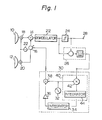
- Figure 1 is a circuit diagram of a space diversity system embodying the present invention;
- Figures 2-3 are signal vector diagrams demonstrating the operation of the system shown in Figure 1; and
- Figure 4 is a modification of the space diversity system shown in Figure 1.
- While the space diversity system of the present invention is susceptible of numerous physical embodiment, depending upon the environment and requirements of use, a substantial number of the herein shown and described embodiments have been made, tested and used, and all have performed in an eminently satisfactory manner.
- Referring to Figure 1 of the drawings, the space diversity system includes
antennas variable phase shifter 16,mixers demodulator 22 demodulates a signal prepared by combining outputs of theantennas demodulator 22 is fed to anidentification circuit 24 as well as to anerror detector 26. While theidentification circuit 24 identifies the digital signal, theerror detector 26 determines the absolute value of an error or difference e between the input and the output of theidentification circuit 24. The output Jet of theerror detector 26 increases with an increase in interference wave and with an increase in noise. Therefore, where two input signals are different in phase by 180 degrees from each other as shown in Figure 2, the error detector output !ei grows extremely large due to an increase in noise. In this instance, it is possible to increase the combined signal level beyond the interference wave and thereby cut down the influence of noise by controlling thephase shifter 16 with the output of theerror detector 26 in such a manner as to accommodate some interference wave, as shown in Figure 3. The regular identified output of thedemodulator 22 appears at aterminal 28. The output of thedemodulator 22 is a baseband signal identical with a signal which was sent out from a transmitter. Concerning the 4-phase shift keying (PSK) system, for example, four signals (I+j), (I-j), (-I+j) and (-I-j) will be produced from thedemodulator 22. If noise is superposed on the input signal, noise will of course be outputted from thedemodulator 22 together with the signal. - Where the phase control on the
variable phase shifter 16 is performed in a direction for minimizing the output of theerror detector 26 as described above, desirable controls will occur for all the signal input conditions at theantennas - The
control section 30 will be described hereinafter. Suppose that an interference wave E2 at theantenna 12 has a phase which is deviated φe (rad) from a value giving E1+E2=0, as illustrated in Figure 3. What is required here is to condition the phase shift ϕs of thephase shifter 16 as
- Initially, the phase shift φs is not optimized and, therefore, includes a deviation ed (rad) as expressed by

- When perturbation εo. sin wot is given to the phase shift φs (where eo>0),

- Thus, based on the perturbation εo. sinwot, the absolute value lei of the intersymbol interference undergoes a variation as produced by

- The correlation R between the absolute value |e| and the perturbation signal εo·sinωot is expressed as

- Because eo . β is positive in sign, it will be seen from the above equation that the correlation R is common in sign to sd. This in turn teaches that the control over the phase shift ϕs needs only be such that it increases or and decreases in the opposite direction to the polarity of the correlation R. It should be noted that the sinusoidal change due to the perturbation proceeds faster than a change derived from the control according to the polarity of the correlation R and, in the average sense, it is zero, the perturbation in effect making no contribution to the essential value of the phase shift φs. Accordingly,


- The principle of operation of the
control section 30 will be understood from the above description. As shown in Figure 1, thecontrol section 30 comprises anoscillator 32 for generating the perturbation εo·sinωot, anintegrator 34 for control, and apolarity reversing circuit 36. Anadder 38 functions to add a perturbance signal to a control signal for a voltage controlled oscillator. Acorrelation circuit 40 comprises amultiplier 42 and anintegrator 44 and serves to determine a correlation R between the perturbance signal and the output of theerror detector 26. Theintegrator 44, however, does not constitute any essential part of the circuit and may be omitted, if desired. The output of theadder 38 is the control signal for controlling the phase of thephase shifter 16. - In summary, it will be seen that the present invention provides a space diversity system which minimizes identification errors by the way the
variable phase shifter 16 is controlled by theerror detector 26. - Figure 4 shows a modified space diversity system shown in Figure 1 where the perturbation amplitude so in the perturbation εo. sinwot is controlled according to the output level of the
error detector 26. If the output level of theerror detector 26 is large, the perturbation amplitude so is set large so as to detect the correlation R easily. On the other hand, if it is an inverse case, the so is set small so that this perturbation may not generate a large signal output jitter. - This function is performed by a combination of a
lowpass filter 45 and amultiplier 46. Thelowpass filter 45 smooths the output of theerror detector 26 and makes the output proportional to the error level. Themultiplier 46 modifies the oscillator output according to the output of thelow pass filter 45. - Various modifications will become possible for those skilled in the art after receiving the teachings of the present disclosure without departing from the scope thereof.
Claims (2)
Applications Claiming Priority (2)
| Application Number | Priority Date | Filing Date | Title |
|---|---|---|---|
| JP122716/82 | 1982-07-14 | ||
| JP57122716A JPS5913442A (en) | 1982-07-14 | 1982-07-14 | Minimum signal dispersion type space diversity device |
Publications (3)
| Publication Number | Publication Date |
|---|---|
| EP0099112A2 EP0099112A2 (en) | 1984-01-25 |
| EP0099112A3 EP0099112A3 (en) | 1984-03-07 |
| EP0099112B1 true EP0099112B1 (en) | 1985-11-21 |
Family
ID=14842821
Family Applications (1)
| Application Number | Title | Priority Date | Filing Date |
|---|---|---|---|
| EP83106831A Expired EP0099112B1 (en) | 1982-07-14 | 1983-07-12 | Space diversity system |
Country Status (6)
| Country | Link |
|---|---|
| US (1) | US4498885A (en) |
| EP (1) | EP0099112B1 (en) |
| JP (1) | JPS5913442A (en) |
| AU (1) | AU563228B2 (en) |
| CA (1) | CA1210073A (en) |
| DE (1) | DE3361292D1 (en) |
Families Citing this family (13)
| Publication number | Priority date | Publication date | Assignee | Title |
|---|---|---|---|---|
| JPS59230334A (en) * | 1983-06-13 | 1984-12-24 | Fujitsu Ltd | Space diversity reception system |
| DE3510580A1 (en) * | 1985-03-23 | 1986-09-25 | Blaupunkt-Werke Gmbh, 3200 Hildesheim | METHOD AND CIRCUIT FOR IMPROVING THE RECEPTION OF RADIO WAVES |
| US4736455A (en) * | 1985-12-23 | 1988-04-05 | Nippon Telegraph And Telephone Corporation | Interference cancellation system |
| DE3641109A1 (en) * | 1986-12-02 | 1988-08-25 | Lindenmeier Heinz | SIGNAL DIVERSITY SYSTEM FOR MOBILE RECEPTION |
| DE4012199C2 (en) * | 1990-04-14 | 1994-03-17 | Ant Nachrichtentech | Method and arrangement for receiving multiple signals according to the diversity principle |
| US5722049A (en) * | 1995-12-05 | 1998-02-24 | Ericsson Inc. | Mobile-link system for a radio communication system wherein diversity combining is performed only for edge/boundary zone signals and not for central zone signals |
| US7046653B2 (en) * | 1998-05-01 | 2006-05-16 | Jan Nigrin | Diversity communication system and method of operation thereof |
| US6704557B1 (en) * | 1999-04-22 | 2004-03-09 | Lucent Technologies Inc. | System and method for protecting a receiver from jamming interference |
| US6911947B1 (en) | 1999-09-08 | 2005-06-28 | Thomson Licensing S.A. | Method and apparatus for reducing multipath distortion in a television signal |
| DE60043312D1 (en) * | 1999-09-08 | 2009-12-24 | Thomson Licensing | Multi-element loop antenna |
| US7447284B2 (en) * | 2003-03-28 | 2008-11-04 | Freescale Semiconductor, Inc. | Method and apparatus for signal noise control |
| EP2768153B1 (en) * | 2011-10-28 | 2019-05-08 | Huawei Technologies Co., Ltd. | Full-duplex communication device and method |
| US9444505B2 (en) * | 2014-04-11 | 2016-09-13 | Broadcom Corporation | System and method for frequency reuse for wireless point-to-point backhaul |
Family Cites Families (5)
| Publication number | Priority date | Publication date | Assignee | Title |
|---|---|---|---|---|
| US4326294A (en) * | 1979-02-13 | 1982-04-20 | Nippon Telegraph & Telephone Public Corporation | Space diversity reception system having compensation means of multipath effect |
| US4278978A (en) * | 1979-09-18 | 1981-07-14 | Nasa | Baseband signal combiner for large aperture antenna array |
| DE3110602C2 (en) * | 1980-03-28 | 1985-07-04 | Nippon Telegraph & Telephone Public Corp., Tokio/Tokyo | Interference compensation system |
| JPS5792931A (en) * | 1980-11-28 | 1982-06-09 | Fujitsu Ltd | Space diversity receiving device |
| US4373210A (en) * | 1981-03-27 | 1983-02-08 | Bell Telephone Laboratories, Incorporated | Space diversity combiner |
-
1982
- 1982-07-14 JP JP57122716A patent/JPS5913442A/en active Pending
-
1983
- 1983-07-11 US US06/512,649 patent/US4498885A/en not_active Expired - Lifetime
- 1983-07-12 EP EP83106831A patent/EP0099112B1/en not_active Expired
- 1983-07-12 DE DE8383106831T patent/DE3361292D1/en not_active Expired
- 1983-07-13 CA CA000432387A patent/CA1210073A/en not_active Expired
- 1983-07-13 AU AU16809/83A patent/AU563228B2/en not_active Ceased
Also Published As
| Publication number | Publication date |
|---|---|
| AU563228B2 (en) | 1987-07-02 |
| DE3361292D1 (en) | 1986-01-02 |
| AU1680983A (en) | 1984-01-19 |
| JPS5913442A (en) | 1984-01-24 |
| CA1210073A (en) | 1986-08-19 |
| US4498885A (en) | 1985-02-12 |
| EP0099112A3 (en) | 1984-03-07 |
| EP0099112A2 (en) | 1984-01-25 |
Similar Documents
| Publication | Publication Date | Title |
|---|---|---|
| EP0099112B1 (en) | Space diversity system | |
| US4484337A (en) | Carrier wave regenerating circuit | |
| US5448602A (en) | Diversity radio receiver | |
| CA2173530C (en) | Modulation and demodulation method, modulator and demodulator | |
| EP0718971A2 (en) | Receiver with automatic frequency control | |
| US4682117A (en) | Quadrature demodulation data receiver with phase error correction | |
| US4079379A (en) | Null steering apparatus for a multiple antenna array | |
| CA1230649A (en) | Interference canceller loop having automatic nulling of the loop phase shift for use in a reception system | |
| EP0120416B1 (en) | Demodulator with automatic gain control circuit | |
| US3109143A (en) | Synchronous demodulator for radiotelegraph signals with phase lock for local oscillator during both mark and space | |
| US4477913A (en) | Automatic equalizer apparatus | |
| GB1580921A (en) | Phase demodulator with offset frequency reference oscillator | |
| US5432819A (en) | DPSK communications with Doppler compensation | |
| US5787124A (en) | Quadrature detector and amplitude error correction method for quadrature detector | |
| EP0099113B2 (en) | Interference cancellation type space diversity system | |
| US4881049A (en) | QAM modulator/demodulator | |
| JPS6347313B2 (en) | ||
| JPS5918900B2 (en) | demodulator | |
| US4099130A (en) | Phase synchronizing circuit | |
| US6091789A (en) | Method and device for phase modulated signals | |
| US5982200A (en) | Costas loop carrier recovery circuit using square-law circuits | |
| US6246730B1 (en) | Method and arrangement for differentially detecting an MPSK signal using a plurality of past symbol data | |
| EP0293828B1 (en) | Circuit device for demodulating DSB modulated signals and method therefor | |
| EP0221476B1 (en) | Television interference-compensation apparatus for phase and amplitude compensation | |
| JP2734137B2 (en) | Dual polarization receiving system |
Legal Events
| Date | Code | Title | Description |
|---|---|---|---|
| PUAI | Public reference made under article 153(3) epc to a published international application that has entered the european phase |
Free format text: ORIGINAL CODE: 0009012 |
|
| PUAL | Search report despatched |
Free format text: ORIGINAL CODE: 0009013 |
|
| AK | Designated contracting states |
Designated state(s): DE FR GB |
|
| AK | Designated contracting states |
Designated state(s): DE FR GB |
|
| 17P | Request for examination filed |
Effective date: 19840227 |
|
| GRAA | (expected) grant |
Free format text: ORIGINAL CODE: 0009210 |
|
| AK | Designated contracting states |
Designated state(s): DE FR GB |
|
| ET | Fr: translation filed | ||
| REF | Corresponds to: |
Ref document number: 3361292 Country of ref document: DE Date of ref document: 19860102 |
|
| PLBE | No opposition filed within time limit |
Free format text: ORIGINAL CODE: 0009261 |
|
| STAA | Information on the status of an ep patent application or granted ep patent |
Free format text: STATUS: NO OPPOSITION FILED WITHIN TIME LIMIT |
|
| 26N | No opposition filed | ||
| PGFP | Annual fee paid to national office [announced via postgrant information from national office to epo] |
Ref country code: GB Payment date: 19950707 Year of fee payment: 13 |
|
| PGFP | Annual fee paid to national office [announced via postgrant information from national office to epo] |
Ref country code: FR Payment date: 19950725 Year of fee payment: 13 |
|
| PGFP | Annual fee paid to national office [announced via postgrant information from national office to epo] |
Ref country code: DE Payment date: 19950929 Year of fee payment: 13 |
|
| PG25 | Lapsed in a contracting state [announced via postgrant information from national office to epo] |
Ref country code: GB Effective date: 19960712 |
|
| GBPC | Gb: european patent ceased through non-payment of renewal fee |
Effective date: 19960712 |
|
| PG25 | Lapsed in a contracting state [announced via postgrant information from national office to epo] |
Ref country code: FR Effective date: 19970328 |
|
| PG25 | Lapsed in a contracting state [announced via postgrant information from national office to epo] |
Ref country code: DE Effective date: 19970402 |
|
| REG | Reference to a national code |
Ref country code: FR Ref legal event code: ST |