EP0098116A2 - Surface acoustic device - Google Patents
Surface acoustic device Download PDFInfo
- Publication number
- EP0098116A2 EP0098116A2 EP83303644A EP83303644A EP0098116A2 EP 0098116 A2 EP0098116 A2 EP 0098116A2 EP 83303644 A EP83303644 A EP 83303644A EP 83303644 A EP83303644 A EP 83303644A EP 0098116 A2 EP0098116 A2 EP 0098116A2
- Authority
- EP
- European Patent Office
- Prior art keywords
- surface acoustic
- strips
- acoustic wave
- electromechanical coupling
- wave device
- Prior art date
- Legal status (The legal status is an assumption and is not a legal conclusion. Google has not performed a legal analysis and makes no representation as to the accuracy of the status listed.)
- Granted
Links
Images


Classifications
-
- H—ELECTRICITY
- H03—ELECTRONIC CIRCUITRY
- H03H—IMPEDANCE NETWORKS, e.g. RESONANT CIRCUITS; RESONATORS
- H03H9/00—Networks comprising electromechanical or electro-acoustic devices; Electromechanical resonators
- H03H9/02—Details
- H03H9/02535—Details of surface acoustic wave devices
- H03H9/02637—Details concerning reflective or coupling arrays
- H03H9/02685—Grating lines having particular arrangements
- H03H9/02771—Reflector banks
-
- H—ELECTRICITY
- H03—ELECTRONIC CIRCUITRY
- H03H—IMPEDANCE NETWORKS, e.g. RESONANT CIRCUITS; RESONATORS
- H03H9/00—Networks comprising electromechanical or electro-acoustic devices; Electromechanical resonators
- H03H9/46—Filters
- H03H9/64—Filters using surface acoustic waves
- H03H9/6423—Means for obtaining a particular transfer characteristic
- H03H9/643—Means for obtaining a particular transfer characteristic the transfer characteristic being determined by reflective or coupling array characteristics
Definitions
- the present invention relates to a surface acoustic wave (SAW) device comprising an input-side transducer, an output-side transducer, and an electromechanical coupling means provided therebetween so as to change the propagation path of the surface acoustic wave. More particulary, it relates to an SAW device wherein the electromechanical coupling means is formed in a given shape to obtain the desired stopband characteristics.
- SAW surface acoustic wave
- SAW devices in accordance with the present invention can be used as filtering devices, signal delaying devices, or the like.
- SAW devices comprising an include electromechanical coupling meansjelements called multi--strip lines (or coupler) which consist of a plurality of electrically conductive strips provided between an input-side transducer and an output-side transducer such as to apply the essential surface acoustic waves emitted from the input-side transducer to the output-side transducer and prevent the bulk wave from being applied to the output-side transducer (e.g.) USP 3739290 and USP 3836876) are already known.
- multi--strip lines or coupler
- FIG 1 is a plan view of an example of a prior art SAW device.
- a SAW device 1 comprises a piezoelectric substrate 11 consisting, for example, of lithium niobium oxide (LiNbO 3 ), an input transducer 16 formed on the surface of the substrate 11; an output transducer 18 formed on the surface of the substrate 11, and the coupler 20 provided between the input transducer 16 and the output transducer 18.
- the input transducer 16 comprises interdigital electrodes 12 and 14, as shown in Fig. 1.
- the output transducer 18 is formed in a manner similar to the input transducer 16.
- surface acoustic waves W are-generated in the surface region of the piezoelectric substrate 11 and propagate in the direction shown in Fig. 1 (the surface acoustic waves propagating in the opposite direction are not shown).
- the surface acoustic waves W may include essential surface acoustic waves as well as bulk waves, which may exert an adverse influence on device performance, such as its filtering.characteristics. It is preferable that the bulk waves not be applied to the output transducer 18.
- the coupler 20 is provided so that only the essential wave component is received, and an electrical potential induced at the coupler 20 in response to the received wave. This potential once again generates surface acousticcaves.
- the coupler 20 includes a plurality of conductive strips 22 formed on the surface of the substrate 11 and in parallel to each other, each of which induces a voltage in response to the waveform signal of the essential component of the surface acoustic waves W.
- the bulk waves Wb cannot be caught at the strips 22 and propagate forward.
- the voltages induced at the conductive strips 22 are transmitted to the opposite ends of the strips, where the strips are associated with the substrate 11 so as to generate a secondary surface acoustic wave W'.
- the output transducer 18 receives the secondary surface acoustic wave W' and outputs an electrical signal in response to the received wave W '.
- the direction of propagation is changed by the coupler 20 as shown and only the essential surface component of the wave is applied to the output transducer 18. This gives the required characteristics, such as a signal delaying feature between the input transducer 16 and the output transducer 18.
- the coupler 20 mentioned above has a considerably large
- SAW devices in the prior art therefore have such drawbacks as an inability to obtain given filtering characteristics. This is the case, for example, with filters used in television sets, which have a deep trap level on both of the band passes.
- An object of the present invention is to provide a surface acoustic wave device that maintains the ability to avoid the influence of the bulk wave and transmit only the essential surface wave, and that provides given filtering characteristics using relatively simple technology.
- a surface acoustic wave device comprising: a piezoelectric substrate; a first electrode means having a set of interdigitated electrodes formed on the surface of the substrate and generating surface acoustic waves on the surface region of the substrate when a high-frequency AC voltage is applied between the two interdigitated electrodes; a second electrode means having two interdigitated electrodes formed on the surface of the substrate, the centre of the second electrode means being spaced at a distance from the centre of the first electrode means in the direction of surface acoustic wave propagation, and generating an electrical signal between the interdigitated electrodes in response to the received surface acoustic waves; and an electromechanical coupling means having a plurality of electrically conductive strips formed on the substrate between the first electrode means and the second electrode means and oriented perpendicular to the direction of surface acoustic wave propagation, the strips being parallel to each other, characterized in that a desired filtering characteristic is obtained by spacing the parallel strips of the coupling means at
- a surface acoustic wave (SAW) device 1 comprises a piezoelectric substrate 11 consisting of, for example, lithium niobium oxide (LiNbO 3 ) on which is provided a first set of electrodes 16 serving as an input transducer, a second set of electrode 18 serving as an output transducer, and an electromechanical coupling element 30.
- the electromechanical coupling element 30 comprises a plurality of strips 32 arranged with in parallel each other in a repeating pattern in which two consecutive strips are connected and the following two not connected at the ends thereof adjacent to the second electrode means 18, as shown. The two consecutive unconnected strips are not electrically grounded are and are islated.
- a common connecting strip 31 is normally grounded, but may be not grounded.
- the strips 32 and the common connecting strip 31 may be formed by, for example, a vapor deposition process using a conductive material such as an aluminium (Al).
- Al aluminium
- the two sets of electrodes 16 and 18 may also be formed in this way.
- each strip only-catches the respective surface acoustic waves in accordance with its reception performance, which depends on the wavelength passing through the corresponding strip, and induces an electrical signal. Beyond a certain number of strips, the reception performance tends to decrease. Performance, manufacturing costs, size, and other factors should therefore be taken into account in selecting an optimum strip number.
- the preferred strip number is from approximately 100 to 200, as mentioned later.
- the center-to-center distance p between the longitudinal strips is defined as follows:
- the first set of electrodes 16 and the second set of electrodes 18 have essentially the attenuation characteristic as curve Cl shown in Figure 3A.
- the total performance of the SAW device in Figure 2 is shown as curve C12 in Figure 3B, which is the summation of curves Cl and C2.
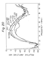
- Figure 5 shows the total frequency_amplitudie characteristics of a SAW device (type: B-e); here, curves B-e-50, 100, 150 and 175 are plotted for 50, 100, 150, and 175 strips, respectively.
- Figure 4 shows the same characteristics as those in Figure 5, obtained in the prior art SAW device shown in Figure 1; here, curves m-25, 50, 100, 150 and 200 represent 25, 50, 100, 150, and 200 strips, respectively.
- first and second stop-bands SBl and SB2 exist at f ⁇ 43 (MHz) and f ⁇ 65 (MHz) on the curves in Fig. 5.
- a general stopband curve in accordance with the present invention is shown as curve C2, while Fig. 6 shows, an actual stopband feature given by the electromechanical coupling element as curve B-e 175.
- Curve B-e 175 has two stopbands, SBl and SB2.
- Curve MSC 100 for an electromechanical coupling element with 100 strips, shows the measured results for the coupler in Figure 1. No stopbands appear here because the coupler has a broad frequency range; i.e., curve MSC 100 is almost flat.
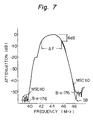
- Curve B-e-176 in Figure 7 shows another actual characteristic of the SAW device shown in Figure 2 and corresponding to the characteristic in Figure 5.
- the conditions of measurement were as follows: strip pitch p mentioned in Expression (1): 20.3 ⁇ m; 176 strips; width of the strip: 2000 A; electrically conductive material: Aluminum (Al); pitch of the interdigital electrodes in the first and set of second electrodes: 22 ⁇ m; substrate: 128°-rotated, Y-cut, X-propagating LiNbO 3 .
- Curve MSC 110 in Fig. 7 is data obtained for a prior device having a distance between strips of 20.9 ⁇ m, and 110 strips.
- Curves B-e 176 and MSC 110 are the total frequency-attenuation characteristics at a center frequency of 44 MHz and a frequency band width of ⁇ 4 MHz.
- Curves MSC 110 and B-e 176 in Figure 7 are similar in shape. However, curve B-e 176 for the device in accordance with the present invention has a distinctive stopband SB at frequency 48.5 MHz. This means that curve B-e 176 has an improved rejection performance compared with curve MSC 110, particularly at higher frequency.
- the SAW device mentioned above is therefore available for use as a filtering device with a center frequency of 44 MHz and a band width of ⁇ 4 MHz.
- a greater number of strips is required in the present invention (170) than in prior art devices (110), as shown in Figure 7. Yet, the SAW device can obtain a similar frequency-attenuation curve at the desired frequency range.
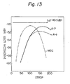
- the relationship between the number of strips and the insertion loss is shown in Fig. 8.
- curve MSC represents the prior art device
- curve B-e the SAW device in accordance with the present invention
- straight line L 0 represents that of an SAW device without an intermediate electromechanical coupling element.
- Line L 0 has a constant loss -49.5 dB.
- the preferred number of strips in the SAW device shown in Figure 2 ranges from approximately 100 to 200.
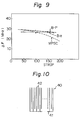
- Fig. 9 shows the relationship between the frequency band width AF, which has a frequency range of 6 dB down from the maximum value in Fig. 7, and the number of strips.
- curve MPSC represents the prior device
- curve B-e represents the SAW device in accordance with the present invention. It is clear that curve B-e has a lower frequency dependence than the prior art device.
- the SAW device of the present invention shown in Figure 2 requires more strips than in the prior art device in order to obtain the same basic performance, with the exception of the stopband properties.
- the SAW device in accordance with the present invention can obtain the predetermined stopbands of the predetermined frequencies through the formation of an electromechanical coupling element 30 which contains strips connected in a given manner and at a given distance from each other, depending on expression 1.
- the SAW device in accordance with the present invention can thus be used as high-performance filters, such as high performance bandpass filters having two stop-bands in television sets, selective rejection filters of a predetermined frequencies, and in other applications.
- the SAW device shown in Fig. 2 is no more difficult to manufacture than devices according to the prior art, and entails about the same manufacturing costs and time.
- Fig. 10 shows an alternative embodiment of electromechanical coupling element 30 in Fig. 2 as an electromechanical coupling element 40.
- This coupling element 40 has a plurality of electrically conductive strips 42 arranged in parallel.
- alternate strips are connected by a common connecting strip 41 at the strip ends near the second set of electrodes 18 (not shown).
- the common connecting strip 41 is grounded; however, strip 41 may not be grounded, the effect obtained thereby being similar.
- Other features of the SAW device are the same as those mentioned above.
- the SAW device provided with electromechanical coupling element 40 can be defined by the following relationship;
- the SAW device provided with the electromechanical coupling means 40 performs as shown in curve A-e in Figs. 11 to 14.
- the measuring conditions are substantially the same as those for the SAW device in Fig. 2.
- Characteristics curves A-e in Fig. 11 correspond to those in Fig. 5, but have only one stopband SB.
- Stopband characteristic cqrve A-e 175 in Fig. 12 corresponds to that in Fig. 6.
- Curve A-e in Fig. 13 corresponds to that in Fig. 8.
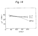
- Curve A-e in Fig. 14 corresponds to that in Fig. 9.
- SAW devices provided with electromechanical coupling means 40 also have suitable stopbands in the same manner as the SAW device in Fig. 2, and maintained the basic performance characteristics of the prior art devices.
- the preferred number of strips of the SAW device mentioned above ranges from approximately 100 to 200.
- Electromechanical coupling elements 50 and 60 in Figs. 15 and 16 have the same connection as the electromechanical coupling elements 30 shown in F ig. 2 However, connecting strips 51 1 to 51 n and 61 1 to 61 n thereof are located at different longitudinal positions. Strips 51 1 to 51 n are positioned at the middle of the strips 52 and the strips 611 to 61 n are arranged arbitrarily.
- SAW devices containing an electromechanical coupling element 50 or 60 depend on substantially the same principle as does the device in Fig. 2 (B-e type).
- the measured performances of devices provided with electromechanical coupling means 50 or 60 are shown as curves B-p in Fig. 17 corresponding to Fig. 5, and curves B-p in Figs. 8 and 9.
- Figs. 18 and 19 are shown in Figs. 18 and 19.
- the electromechanical coupling elements 70 and 80 in Figs. 18 and 19 have the same connections as the electromechanical coupling means 40 shown in Figure 10. However, connecting strips 7 1 1 to 71 n and 811 to 81 n thereof are located at different longitudinal positions. Strips 71 l to 71 are positioned at the middle of the strips 72 and strips 81 1 to 81 n are located at arbitrary positions. n
- SAW devices with electromechanical coupling elements 70 or 80 depends basically on the same principle as the devices in Fig. 10 described above (type A-e).
- the performances of the devices provided with electromechanical coupling means 70 or 80 were measured as curves A-p in Fig. 20, which corresponds to Fig. 11, and curves A-p in Figs. 12 to 14.
Abstract
Description
- The present invention relates to a surface acoustic wave (SAW) device comprising an input-side transducer, an output-side transducer, and an electromechanical coupling means provided therebetween so as to change the propagation path of the surface acoustic wave. More particulary, it relates to an SAW device wherein the electromechanical coupling means is formed in a given shape to obtain the desired stopband characteristics.
- SAW devices in accordance with the present invention can be used as filtering devices, signal delaying devices, or the like.
- Surface acoustic wave (SAW) devices comprising an include electromechanical coupling meansjelements called multi--strip lines (or coupler) which consist of a plurality of electrically conductive strips provided between an input-side transducer and an output-side transducer such as to apply the essential surface
acoustic waves emitted from the input-side transducer to the output-side transducer and prevent the bulk wave from being applied to the output-side transducer (e.g.) USP 3739290 and USP 3836876) are already known. - Figure 1 is a plan view of an example of a prior art SAW device. In Figure 1, a
SAW device 1 comprises apiezoelectric substrate 11 consisting, for example, of lithium niobium oxide (LiNbO3), aninput transducer 16 formed on the surface of thesubstrate 11; anoutput transducer 18 formed on the surface of thesubstrate 11, and thecoupler 20 provided between theinput transducer 16 and theoutput transducer 18. Theinput transducer 16 comprisesinterdigital electrodes output transducer 18 is formed in a manner similar to theinput transducer 16. - When a high-frequency AC power source is applied to the
electrodes input transducer 16, surface acoustic waves W are-generated in the surface region of thepiezoelectric substrate 11 and propagate in the direction shown in Fig. 1 (the surface acoustic waves propagating in the opposite direction are not shown). The surface acoustic waves W may include essential surface acoustic waves as well as bulk waves, which may exert an adverse influence on device performance, such as its filtering.characteristics. It is preferable that the bulk waves not be applied to theoutput transducer 18. Thecoupler 20 is provided so that only the essential wave component is received, and an electrical potential induced at thecoupler 20 in response to the received wave. This potential once again generates surface acousticcaves. W', which are applied to theoutput transducer 18. Thecoupler 20 includes a plurality ofconductive strips 22 formed on the surface of thesubstrate 11 and in parallel to each other, each of which induces a voltage in response to the waveform signal of the essential component of the surface acoustic waves W. The bulk waves Wb cannot
be caught at thestrips 22 and propagate forward. The voltages induced at theconductive strips 22 are transmitted to the opposite ends of the strips, where the strips are associated with thesubstrate 11 so as to generate a secondary surface acoustic wave W'. Theoutput transducer 18 receives the secondary surface acoustic wave W' and outputs an electrical signal in response to the received wave W'. As mentioned above, the direction of propagation is changed by thecoupler 20 as shown and only the essential surface component of the wave is applied to theoutput transducer 18. This gives the required characteristics, such as a signal delaying feature between theinput transducer 16 and theoutput transducer 18. - The
coupler 20 mentioned above has a considerably - wide frequency bandwith. SAW devices in the prior art therefore have such drawbacks as an inability to obtain given filtering characteristics. This is the case, for example, with filters used in television sets, which have a deep trap level on both of the band passes.
- An object of the present invention is to provide a surface acoustic wave device that maintains the ability to avoid the influence of the bulk wave and transmit only the essential surface wave, and that provides given filtering characteristics using relatively simple technology.
- According to the present invention, there is provided a surface acoustic wave device comprising: a piezoelectric substrate; a first electrode means having a set of interdigitated electrodes formed on the surface of the substrate and generating surface acoustic waves on the surface region of the substrate when a high-frequency AC voltage is applied between the two interdigitated electrodes; a second electrode means having two interdigitated electrodes formed on the surface of the substrate, the centre of the second electrode means being spaced at a distance from the centre of the first electrode means in the direction of surface acoustic wave propagation, and generating an electrical signal between the interdigitated electrodes in response to the received surface acoustic waves; and an electromechanical coupling means having a plurality of electrically conductive strips formed on the substrate between the first electrode means and the second electrode means and oriented perpendicular to the direction of surface acoustic wave propagation, the strips being parallel to each other, characterized in that a desired filtering characteristic is obtained by spacing the parallel strips of the coupling means at a selected distance fron one another and by interconnecting selected ones of the strips of the coupling means.
- Other objects and features of the present invention will be described in detail with reference to the accompanying drawings.
- In the drawings:
- Fig. 1 illustrates a plan view of an example of a prior surface acoustic wave (SAW) device provided with an electromechanical coupling means;
- Fig. 2 illustrates a plan view of an embodiment of a SAW device in accordance with the present invention;
- Figs. 3A and 3B show a principal gain attenuation characteristic of a SAW device in accordance with the present invention;
- Fig. 4 shows an actual gain attenuation characteristic taken by the SAW device shown in Fig. 1;
- Fig. 5 shows an actual gain attenuation characteristic obtained by the SAW device shown in Fig. 2;
- Fig. 6 shows a stopband feature gained by the electromechanical coupling means forming on the SAW device in Fig. 2;
- Fig. 7 shows a total filtering characteristic obtained by the SAW device shown in Fig. 2;
- Fig. 8 shows plots of insertion losses versus the number of the strips in the electromechanical coupling means of the SAW device in Fig. 2;
- Fig. 9 shows plots of the frequency band versus the number of strips in the SAW device in Fig. 2;
- Fig. 10 illustrates a plan view of another embodiment of the electromechanical coupling means of the SAW device shown in Fig. 2;
- Fig. 11 shows the total attenuation in accordance with the SAW device using the electromechanical coupling means;
- Fig. 12 shows the characteristic curves .corresponding to the curves in Fig. 6 for the electromechanical coupling means;
- Fig. 13 shows the characteristic curves corresponding to the Fig. 8 for the SAW device using the electromechanical coupling means shown in Fig. 10;
- Fig. 14 shows the characteristic curves corresponding to the curves in Fig. 9 for the SAW device used in the electromechanical coupling means shown in Fig. 10;
- Figs. 15 and 16 are plan views of another embodiments of the electromechanical coupling means of the SAW device shown in Fig. 2;
- Fig. 17 represents the attenuation characteristics of the SAW device using the electromechanical coupling means of Figs. 15 and 16;
- Figs. 18 and 19 illustrate plan views of other embodiments of the electromechanical coupling means of the SAW device shown in Fig. 2; and
- Fig. 20 shows the filtering characteristics of the SAW device using the electromechanical coupling means of Figs. 18 and 19.
- One example of the present invention is shown in Fig. 2. Here, a surface acoustic wave (SAW)
device 1 comprises apiezoelectric substrate 11 consisting of, for example, lithium niobium oxide (LiNbO3) on which is provided a first set ofelectrodes 16 serving as an input transducer, a second set ofelectrode 18 serving as an output transducer, and anelectromechanical coupling element 30. Theelectromechanical coupling element 30 comprises a plurality of strips 32 arranged with in parallel each other in a repeating pattern in which two consecutive strips are connected and the following two not connected at the ends thereof adjacent to the second electrode means 18, as shown. The two consecutive unconnected strips are not electrically grounded are and are islated. A common connectingstrip 31 is normally grounded, but may be not grounded. The strips 32 and the common connectingstrip 31 may be formed by, for example, a vapor deposition process using a conductive material such as an aluminium (Al). The two sets ofelectrodes - There are provided a plurality of parallel strips 32, the exact number of which depends on the desired reception performance of the surface acoustic waves. In general, many strips are required, because each strip only-catches the respective surface acoustic waves in accordance with its reception performance, which depends on the wavelength passing through the corresponding strip, and induces an electrical signal. Beyond a certain number of strips, the reception performance tends to decrease. Performance, manufacturing costs, size, and other factors should therefore be taken into account in selecting an optimum strip number. In this example, the preferred strip number is from approximately 100 to 200, as mentioned later.
- When n stop bands are required, the center-to-center distance p between the longitudinal strips is defined as follows:

- where, v: propagation speed of the surface acoustic wave,
- fm: center frequency at the required stop band.
- When the pitch p between the strips is defined on the basis of the above relationship, the desired electromechanical coupling element can be formed, this having, for example, one stop band (n = 1) or two stop bands (n = 2). When n = 2, a principal characteristic of stop bands SBl, SB2 is shown in Figure 3A as curve C2. On the other hand, the first set of
electrodes 16 and the second set ofelectrodes 18 have essentially the attenuation characteristic as curve Cl shown in Figure 3A. The total performance of the SAW device in Figure 2 is shown as curve C12 in Figure 3B, which is the summation of curves Cl and C2. - The measured performances of the example mentioned above with reference to the SAW device in Figure 2 (type: B-e) are shown in Figs. 5-9. Measurements were carried at under the following conditions. Substrate: 128°-rotated Y-cut, X-propagating LiNbO3; the interdigital electrodes of the first and second set of
electrodes - Figure 5 shows the total frequency_amplitudie characteristics of a SAW device (type: B-e); here, curves B-e-50, 100, 150 and 175 are plotted for 50, 100, 150, and 175 strips, respectively. In Figure 5, attenuation relative to the maximum value, i.e., A ref = 50.5 dB, is plotted on the vertical axis and frequency on the horizontal axis.
- Figure 4 shows the same characteristics as those in Figure 5, obtained in the prior art SAW device shown in Figure 1; here, curves m-25, 50, 100, 150 and 200 represent 25, 50, 100, 150, and 200 strips, respectively.
- From a comparison of the characteristics shown in the curves in.Figs. 4 and 5, it is apparent that first and second stop-bands SBl and SB2 exist at f ≒ 43 (MHz) and f ≒ 65 (MHz) on the curves in Fig. 5.
- In Fig. 3, a general stopband curve in accordance with the present invention is shown as curve C2, while Fig. 6 shows, an actual stopband feature given by the electromechanical coupling element as
curve B-e 175.Curve B-e 175 has two stopbands, SBl and SB2.Curve MSC 100, for an electromechanical coupling element with 100 strips, shows the measured results for the coupler in Figure 1. No stopbands appear here because the coupler has a broad frequency range; i.e.,curve MSC 100 is almost flat. - Curve B-e-176 in Figure 7 shows another actual characteristic of the SAW device shown in Figure 2 and corresponding to the characteristic in Figure 5. The conditions of measurement were as follows: strip pitch p mentioned in Expression (1): 20.3 µm; 176 strips; width of the strip: 2000 A; electrically conductive material: Aluminum (Al); pitch of the interdigital electrodes in the first and set of second electrodes: 22 µm; substrate: 128°-rotated, Y-cut, X-propagating LiNbO3.
Curve MSC 110 in Fig. 7 is data obtained for a prior device having a distance between strips of 20.9 µm, and 110 strips. Curves B-e 176 andMSC 110 are the total frequency-attenuation characteristics at a center frequency of 44 MHz and a frequency band width of ±4 MHz. -
Curves MSC 110 and B-e 176 in Figure 7 are similar in shape. However,curve B-e 176 for the device in accordance with the present invention has a distinctive stopband SB at frequency 48.5 MHz. This means thatcurve B-e 176 has an improved rejection performance compared withcurve MSC 110, particularly at higher frequency. The SAW device mentioned above is therefore available for use as a filtering device with a center frequency of 44 MHz and a band width of ±4 MHz. - A greater number of strips is required in the present invention (170) than in prior art devices (110), as shown in Figure 7. Yet, the SAW device can obtain a similar frequency-attenuation curve at the desired frequency range. The relationship between the number of strips and the insertion loss is shown in Fig. 8. In Fig. 8, curve MSC represents the prior art device, curve B-e the SAW device in accordance with the present invention, and straight line L0 represents that of an SAW device without an intermediate electromechanical coupling element. Line L0 has a constant loss -49.5 dB. As seen from Fig. 8, the preferred number of strips in the SAW device shown in Figure 2 ranges from approximately 100 to 200.
- Fig. 9 shows the relationship between the frequency band width AF, which has a frequency range of 6 dB down from the maximum value in Fig. 7, and the number of strips. In Fig. 9, curve MPSC represents the prior device and curve B-e represents the SAW device in accordance with the present invention. It is clear that curve B-e has a lower frequency dependence than the prior art device.
- As mentioned above, the SAW device of the present invention shown in Figure 2 requires more strips than in the prior art device in order to obtain the same basic performance, with the exception of the stopband properties. The SAW device in accordance with the present invention, however, can obtain the predetermined stopbands of the predetermined frequencies through the formation of an
electromechanical coupling element 30 which contains strips connected in a given manner and at a given distance from each other, depending onexpression 1. - The SAW device in accordance with the present invention can thus be used as high-performance filters, such as high performance bandpass filters having two stop-bands in television sets, selective rejection filters of a predetermined frequencies, and in other applications.
- The SAW device shown in Fig. 2 is no more difficult to manufacture than devices according to the prior art, and entails about the same manufacturing costs and time.
- The principle and scope of the present invention is not limited by the above-described example, which can be accompanied by several other modifications. Several more examples are described below.
- Fig. 10 shows an alternative embodiment of
electromechanical coupling element 30 in Fig. 2 as anelectromechanical coupling element 40. Thiscoupling element 40 has a plurality of electricallyconductive strips 42 arranged in parallel. Here, alternate strips are connected by a common connectingstrip 41 at the strip ends near the second set of electrodes 18 (not shown). In this embodiment, the common connectingstrip 41 is grounded; however,strip 41 may not be grounded, the effect obtained thereby being similar. Other features of the SAW device are the same as those mentioned above. - The SAW device provided with
electromechanical coupling element 40 can be defined by the following relationship;
- where, p': center-to-center distance between the strips;
- m: number of stopbands, m = 1, 2, ---, m,
- V: propagation speed of the surface acoustic wave,
- fT: center frequency at the required stopband.
- The SAW device provided with the electromechanical coupling means 40 (type: A-e) performs as shown in curve A-e in Figs. 11 to 14. The measuring conditions are substantially the same as those for the SAW device in Fig. 2.
- Characteristics curves A-e in Fig. 11 correspond to those in Fig. 5, but have only one stopband SB.
- Stopband characteristic cqrve A-e 175 in Fig. 12 corresponds to that in Fig. 6.
- Curve A-e in Fig. 13 corresponds to that in Fig. 8.
- Curve A-e in Fig. 14 corresponds to that in Fig. 9.
- As seen apparent from the above description and the performance curves in Figs. 11 to 14, SAW devices provided with electromechanical coupling means 40 also have suitable stopbands in the same manner as the SAW device in Fig. 2, and maintained the basic performance characteristics of the prior art devices.
- The preferred number of strips of the SAW device mentioned above ranges from approximately 100 to 200.
- In addition, other embodiments in accordance with the present invention will be shown in Figs. 15 and 16.
Electromechanical coupling elements electromechanical coupling elements 30 shown in Fig. 2 However, connectingstrips 511 to 51n and 611 to 61n thereof are located at different longitudinal positions.Strips 511 to 51n are positioned at the middle of the strips 52 and the strips 611 to 61n are arranged arbitrarily. - SAW devices containing an
electromechanical coupling element 50 or 60 (named B-p type) depend on substantially the same principle as does the device in Fig. 2 (B-e type). The measured performances of devices provided with electromechanical coupling means 50 or 60 are shown as curves B-p in Fig. 17 corresponding to Fig. 5, and curves B-p in Figs. 8 and 9. - other embodiments in accordance with the present invention are shown in Figs. 18 and 19. The
electromechanical coupling elements Strips 71l to 71 are positioned at the middle of the strips 72 and strips 811 to 81n are located at arbitrary positions. n - SAW devices with
electromechanical coupling elements 70 or 80 (A-p type) depends basically on the same principle as the devices in Fig. 10 described above (type A-e). The performances of the devices provided with electromechanical coupling means 70 or 80 were measured as curves A-p in Fig. 20, which corresponds to Fig. 11, and curves A-p in Figs. 12 to 14.
Claims (11)


Applications Claiming Priority (2)
| Application Number | Priority Date | Filing Date | Title |
|---|---|---|---|
| JP57111888A JPS594215A (en) | 1982-06-29 | 1982-06-29 | Surface acoustic wave device |
| JP111888/82 | 1982-06-29 |
Publications (3)
| Publication Number | Publication Date |
|---|---|
| EP0098116A2 true EP0098116A2 (en) | 1984-01-11 |
| EP0098116A3 EP0098116A3 (en) | 1985-10-09 |
| EP0098116B1 EP0098116B1 (en) | 1989-04-12 |
Family
ID=14572655
Family Applications (1)
| Application Number | Title | Priority Date | Filing Date |
|---|---|---|---|
| EP83303644A Expired EP0098116B1 (en) | 1982-06-29 | 1983-06-24 | Surface acoustic device |
Country Status (4)
| Country | Link |
|---|---|
| US (1) | US4551695A (en) |
| EP (1) | EP0098116B1 (en) |
| JP (1) | JPS594215A (en) |
| DE (1) | DE3379624D1 (en) |
Cited By (1)
| Publication number | Priority date | Publication date | Assignee | Title |
|---|---|---|---|---|
| EP0257377A2 (en) * | 1986-08-29 | 1988-03-02 | Siemens Aktiengesellschaft | Surface wave resonator structure comprising reflective finger metallization strips divided into parts |
Families Citing this family (4)
| Publication number | Priority date | Publication date | Assignee | Title |
|---|---|---|---|---|
| US4801836A (en) * | 1987-08-24 | 1989-01-31 | The United States Of America As Represented By The Secretary Of The Army | SAW dispersive delay device |
| DE4447740B4 (en) * | 1993-09-06 | 2008-10-09 | Sanyo Electric Co., Ltd., Moriguchi | Acoustic surface wave filter |
| JP2728023B2 (en) * | 1995-04-28 | 1998-03-18 | 日本電気株式会社 | Adjustment method of surface acoustic wave filter |
| DE102004005129B4 (en) * | 2004-02-02 | 2018-09-27 | Snaptrack, Inc. | Device with sensitive component structures and method of manufacture |
Citations (2)
| Publication number | Priority date | Publication date | Assignee | Title |
|---|---|---|---|---|
| GB1389023A (en) * | 1971-08-05 | 1975-04-03 | Standard Telephones Cables Ltd | Acoustic wave coupler devices |
| US3988703A (en) * | 1975-12-31 | 1976-10-26 | Zenith Radio Corporation | Acoustic surface wave device having split-isolated or split-connected multistrip coupler |
Family Cites Families (4)
| Publication number | Priority date | Publication date | Assignee | Title |
|---|---|---|---|---|
| JPS5172257A (en) * | 1974-12-20 | 1976-06-22 | Toko Inc | DANSEIHYOMENHAFUIRUTA |
| US3987379A (en) * | 1976-01-02 | 1976-10-19 | Zenith Radio Corporation | Acoustic surface wave filter having combined split-isolated and split-connected coupler |
| JPS5834048B2 (en) * | 1978-07-24 | 1983-07-23 | 株式会社村田製作所 | surface acoustic wave device |
| SU945951A1 (en) * | 1979-03-21 | 1982-07-23 | Ордена Трудового Красного Знамени Институт Радиотехники И Электроники Ан Ссср | Filter on surface acoustic waves |
-
1982
- 1982-06-29 JP JP57111888A patent/JPS594215A/en active Granted
-
1983
- 1983-06-24 EP EP83303644A patent/EP0098116B1/en not_active Expired
- 1983-06-24 DE DE8383303644T patent/DE3379624D1/en not_active Expired
- 1983-06-28 US US06/508,546 patent/US4551695A/en not_active Expired - Fee Related
Patent Citations (2)
| Publication number | Priority date | Publication date | Assignee | Title |
|---|---|---|---|---|
| GB1389023A (en) * | 1971-08-05 | 1975-04-03 | Standard Telephones Cables Ltd | Acoustic wave coupler devices |
| US3988703A (en) * | 1975-12-31 | 1976-10-26 | Zenith Radio Corporation | Acoustic surface wave device having split-isolated or split-connected multistrip coupler |
Non-Patent Citations (1)
| Title |
|---|
| ELECTRONICS LETTERS, vol. 8, no. 4, 24th February 1972, pages 81-82, London, GB; J.D. MAINES et al.: "Frequency-dependent behaviour of an acoustic-surface-wave multistrip coupler" * |
Cited By (2)
| Publication number | Priority date | Publication date | Assignee | Title |
|---|---|---|---|---|
| EP0257377A2 (en) * | 1986-08-29 | 1988-03-02 | Siemens Aktiengesellschaft | Surface wave resonator structure comprising reflective finger metallization strips divided into parts |
| EP0257377A3 (en) * | 1986-08-29 | 1989-05-10 | Siemens Aktiengesellschaft Berlin Und Munchen | Surface wave resonator structure comprising reflective finger metallization strips divided into parts |
Also Published As
| Publication number | Publication date |
|---|---|
| JPS594215A (en) | 1984-01-11 |
| US4551695A (en) | 1985-11-05 |
| DE3379624D1 (en) | 1989-05-18 |
| EP0098116A3 (en) | 1985-10-09 |
| EP0098116B1 (en) | 1989-04-12 |
| JPH0145772B2 (en) | 1989-10-04 |
Similar Documents
| Publication | Publication Date | Title |
|---|---|---|
| US4353046A (en) | Surface acoustic wave device with reflectors | |
| US3686518A (en) | Unidirectional surface wave transducers | |
| US4746882A (en) | Saw multiplexer using tapered transducers | |
| US4388600A (en) | Surface acoustic wave device | |
| JPS62188512A (en) | Surface elastic wave resonator, surface elastic wave resonator filter and manufacture of them | |
| US4079342A (en) | Fanned multistrip coupler filters | |
| US4007433A (en) | Elastic surface wave filter | |
| EP0316836B1 (en) | Surface-acoustic-wave device | |
| US4263571A (en) | Surface acoustic wave filter | |
| US4902925A (en) | Reflectionless transducer | |
| EP0098116A2 (en) | Surface acoustic device | |
| US4575696A (en) | Method for using interdigital surface wave transducer to generate unidirectionally propagating surface wave | |
| US4659955A (en) | Surface-propagating acoustic wave device | |
| US4575698A (en) | Surface acoustic wave device | |
| US4365220A (en) | Surface wave circuit device | |
| US4255726A (en) | Surface acoustic wave filter | |
| US4370633A (en) | Acoustic wave bandpass electrical filters | |
| EP0063839B1 (en) | Acoustic wave bandpass electrical filters | |
| EP0074781B1 (en) | Surface acoustic wave filter | |
| EP0255263A2 (en) | Transducer | |
| EP0169607A2 (en) | Surface-propagating acoustic wave device | |
| JPS5997216A (en) | Acoustic surface wave filter | |
| JPS5941915A (en) | Acoustic surface wave device | |
| US20030067370A1 (en) | String weighted surface-acoustic-wave transducer | |
| US4344051A (en) | Elastic surface wave transducer and filter incorporating such a transducer |
Legal Events
| Date | Code | Title | Description |
|---|---|---|---|
| PUAI | Public reference made under article 153(3) epc to a published international application that has entered the european phase |
Free format text: ORIGINAL CODE: 0009012 |
|
| AK | Designated contracting states |
Designated state(s): DE FR GB |
|
| PUAL | Search report despatched |
Free format text: ORIGINAL CODE: 0009013 |
|
| AK | Designated contracting states |
Designated state(s): DE FR GB |
|
| 17P | Request for examination filed |
Effective date: 19860218 |
|
| 17Q | First examination report despatched |
Effective date: 19871012 |
|
| GRAA | (expected) grant |
Free format text: ORIGINAL CODE: 0009210 |
|
| AK | Designated contracting states |
Kind code of ref document: B1 Designated state(s): DE FR GB |
|
| REF | Corresponds to: |
Ref document number: 3379624 Country of ref document: DE Date of ref document: 19890518 |
|
| ET | Fr: translation filed | ||
| PLBE | No opposition filed within time limit |
Free format text: ORIGINAL CODE: 0009261 |
|
| STAA | Information on the status of an ep patent application or granted ep patent |
Free format text: STATUS: NO OPPOSITION FILED WITHIN TIME LIMIT |
|
| 26N | No opposition filed | ||
| PGFP | Annual fee paid to national office [announced via postgrant information from national office to epo] |
Ref country code: GB Payment date: 19900612 Year of fee payment: 8 |
|
| PGFP | Annual fee paid to national office [announced via postgrant information from national office to epo] |
Ref country code: FR Payment date: 19900629 Year of fee payment: 8 |
|
| PGFP | Annual fee paid to national office [announced via postgrant information from national office to epo] |
Ref country code: DE Payment date: 19900821 Year of fee payment: 8 |
|
| PG25 | Lapsed in a contracting state [announced via postgrant information from national office to epo] |
Ref country code: GB Effective date: 19910624 |
|
| GBPC | Gb: european patent ceased through non-payment of renewal fee | ||
| PG25 | Lapsed in a contracting state [announced via postgrant information from national office to epo] |
Ref country code: FR Effective date: 19920228 |
|
| PG25 | Lapsed in a contracting state [announced via postgrant information from national office to epo] |
Ref country code: DE Effective date: 19920401 |