EP0097797A2 - Elektronische Wiedergabevorrichtung - Google Patents
Elektronische Wiedergabevorrichtung Download PDFInfo
- Publication number
- EP0097797A2 EP0097797A2 EP83104484A EP83104484A EP0097797A2 EP 0097797 A2 EP0097797 A2 EP 0097797A2 EP 83104484 A EP83104484 A EP 83104484A EP 83104484 A EP83104484 A EP 83104484A EP 0097797 A2 EP0097797 A2 EP 0097797A2
- Authority
- EP
- European Patent Office
- Prior art keywords
- storage site
- array
- dielectric
- layer
- storage
- Prior art date
- Legal status (The legal status is an assumption and is not a legal conclusion. Google has not performed a legal analysis and makes no representation as to the accuracy of the status listed.)
- Granted
Links
- 238000003860 storage Methods 0.000 claims abstract description 85
- 229910052710 silicon Inorganic materials 0.000 claims abstract description 23
- 239000010703 silicon Substances 0.000 claims abstract description 23
- XUIMIQQOPSSXEZ-UHFFFAOYSA-N Silicon Chemical compound [Si] XUIMIQQOPSSXEZ-UHFFFAOYSA-N 0.000 claims abstract description 22
- OAICVXFJPJFONN-UHFFFAOYSA-N Phosphorus Chemical compound [P] OAICVXFJPJFONN-UHFFFAOYSA-N 0.000 claims abstract description 15
- 230000005669 field effect Effects 0.000 claims abstract description 6
- 239000004065 semiconductor Substances 0.000 claims description 10
- 230000000694 effects Effects 0.000 abstract description 8
- 230000001276 controlling effect Effects 0.000 description 4
- 238000010894 electron beam technology Methods 0.000 description 4
- 238000000034 method Methods 0.000 description 4
- VYPSYNLAJGMNEJ-UHFFFAOYSA-N Silicium dioxide Chemical compound O=[Si]=O VYPSYNLAJGMNEJ-UHFFFAOYSA-N 0.000 description 3
- 230000005855 radiation Effects 0.000 description 3
- 230000009471 action Effects 0.000 description 2
- 230000009286 beneficial effect Effects 0.000 description 2
- 230000008901 benefit Effects 0.000 description 2
- 238000007599 discharging Methods 0.000 description 2
- 230000005684 electric field Effects 0.000 description 2
- 238000005516 engineering process Methods 0.000 description 2
- 238000004519 manufacturing process Methods 0.000 description 2
- 239000011159 matrix material Substances 0.000 description 2
- 238000012986 modification Methods 0.000 description 2
- 230000004048 modification Effects 0.000 description 2
- 229910021420 polycrystalline silicon Inorganic materials 0.000 description 2
- 229920005591 polysilicon Polymers 0.000 description 2
- 238000006424 Flood reaction Methods 0.000 description 1
- 239000004411 aluminium Substances 0.000 description 1
- 229910052782 aluminium Inorganic materials 0.000 description 1
- XAGFODPZIPBFFR-UHFFFAOYSA-N aluminium Chemical compound [Al] XAGFODPZIPBFFR-UHFFFAOYSA-N 0.000 description 1
- 238000005513 bias potential Methods 0.000 description 1
- 239000011248 coating agent Substances 0.000 description 1
- 238000000576 coating method Methods 0.000 description 1
- 238000010276 construction Methods 0.000 description 1
- 238000010586 diagram Methods 0.000 description 1
- 239000003989 dielectric material Substances 0.000 description 1
- 238000009792 diffusion process Methods 0.000 description 1
- NQKXFODBPINZFK-UHFFFAOYSA-N dioxotantalum Chemical compound O=[Ta]=O NQKXFODBPINZFK-UHFFFAOYSA-N 0.000 description 1
- 238000005530 etching Methods 0.000 description 1
- 230000001747 exhibiting effect Effects 0.000 description 1
- 239000010408 film Substances 0.000 description 1
- 230000006872 improvement Effects 0.000 description 1
- 238000009413 insulation Methods 0.000 description 1
- 239000012212 insulator Substances 0.000 description 1
- 238000004020 luminiscence type Methods 0.000 description 1
- 230000014759 maintenance of location Effects 0.000 description 1
- 239000000463 material Substances 0.000 description 1
- 229910052751 metal Inorganic materials 0.000 description 1
- 239000002184 metal Substances 0.000 description 1
- 230000002093 peripheral effect Effects 0.000 description 1
- 230000001105 regulatory effect Effects 0.000 description 1
- 230000004044 response Effects 0.000 description 1
- 230000000717 retained effect Effects 0.000 description 1
- 150000003376 silicon Chemical class 0.000 description 1
- 235000012239 silicon dioxide Nutrition 0.000 description 1
- 239000000377 silicon dioxide Substances 0.000 description 1
- 239000010409 thin film Substances 0.000 description 1
- WFKWXMTUELFFGS-UHFFFAOYSA-N tungsten Chemical compound [W] WFKWXMTUELFFGS-UHFFFAOYSA-N 0.000 description 1
- 229910052721 tungsten Inorganic materials 0.000 description 1
- 239000010937 tungsten Substances 0.000 description 1
Images

Classifications
-
- H—ELECTRICITY
- H01—ELECTRIC ELEMENTS
- H01J—ELECTRIC DISCHARGE TUBES OR DISCHARGE LAMPS
- H01J31/00—Cathode ray tubes; Electron beam tubes
- H01J31/08—Cathode ray tubes; Electron beam tubes having a screen on or from which an image or pattern is formed, picked up, converted, or stored
- H01J31/10—Image or pattern display tubes, i.e. having electrical input and optical output; Flying-spot tubes for scanning purposes
- H01J31/12—Image or pattern display tubes, i.e. having electrical input and optical output; Flying-spot tubes for scanning purposes with luminescent screen
- H01J31/122—Direct viewing storage tubes without storage grid
-
- H—ELECTRICITY
- H01—ELECTRIC ELEMENTS
- H01J—ELECTRIC DISCHARGE TUBES OR DISCHARGE LAMPS
- H01J29/00—Details of cathode-ray tubes or of electron-beam tubes of the types covered by group H01J31/00
- H01J29/02—Electrodes; Screens; Mounting, supporting, spacing or insulating thereof
- H01J29/10—Screens on or from which an image or pattern is formed, picked up, converted or stored
- H01J29/36—Photoelectric screens; Charge-storage screens
- H01J29/39—Charge-storage screens
Definitions
- This invention relates generally to electronic display devices, and more particularly to display devices having the ability to retain displayed information. Such devices are referred to in the art as storage tubes.
- Storage tubes are known in which storage is achieved through the use of a storage mesh in front of a fluorescent screen on which the display is developed.
- a storage dielectric is placed on the storage mesh.
- the signals to be displayed are stored in the form of a charge pattern which exists on the surface of the dielectric as a result of being bombarded selectively by an electron beam.
- a flooding beam which serves as a second source of energy is modulated by the charge pattern on the storage mesh creating the stored image on the fluorescent viewing screen.
- Such storage tubes are bulky, are complicated to manufacture and require complex circuitry to drive them.
- Cathode ray tubes have been arranged to provide storage by controlling the flow of electrons.
- a light responsive material is disposed on a perforated control grid for regulating the flow of electrons therethrough.
- Writing is accomplished by means of radiation selectively discharging a uniform charge.
- the selective radiation discharging means includes a phosphor and means causing an electron beam to impinge thereon whereby selected areas of the phosphor produce radiation.
- US Patent NO.3,473,200 discloses direct-view storage CRT having a collector mesh positioned adjacent a storage target comprising a metallic storage mesh having a film of dielectric coating thereon. According to the patent, writing, reading and erasure are all accomplished by controlling a relatively conventional electron gun which is located at a neck section along the bottom of one edge of the flat screen, adding to the bulk of what is otherwise a relatively flat profile device.
- an electronic display device of the type wherein a mesh collector, and a dielectric storage site array are positioned between an electron source and a phosphor screen, characterised in that said mesh collector and said dielectric storage site array are formed in a semiconductor wafer layer, said semiconductor wafer layer providing an addressable array of transistors, each transistor being associated with a dielectric storage site in said storage site array for controlling the writing of such dielectric storage site, and said addressable array of transistors being arranged to cooperate with said electron source to permit selective writing of said storage site array.
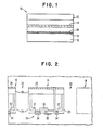
- a preferred embodiment of a flat profile storage CRT 10 of the present invention includes an area electron source 12, and a silicon wafer layer 14 containing an integrated storage structure with an array of switching devices fabricated thereon.
- the silicon wafer 14 is disposed between the area electron source 12 and a viewing screen 16 which has deposited thereon a phosphor layer 18.
- the entire storage CRT 10 is housed in a vacuum envelope not shown.
- the flat profile vacuum fluorescent CRT display 10 has storage capability (to be described hereinafter), and therefore, does not need refresh circuitry. Since the phosphor 18 operates under 100% duty cycle, a display with increased brightness is achieved. Since both the complex storage and writing function of the storage CRT 10 are achieved in an integrated monolithic structure in the form of a silicon wafer 14, the flat storage CRT 10, according to the present invention is inherently simpler to construct, and can be manufactured with substantially lower cost.
- the area electron source 12 of FIG. 1 provides a uniform flooding electron beam having a diameter, for example, at about five inches or larger so as to substantially flood the entire area of the silicon wafer layer 14.
- the cathode (not shown) of the area electron source 12 may be connected to the ground potential.
- Flooding electron guns capable of providing the above described function are known heretofore.
- such an area cathode electron source may be made with tungsten coated with Sr-Ba oxide.
- U. S. Patent 3,975,656, issued to Newton, et al describes the use of such a flooding gun for providing a large area beam in a storage CRT read operation.
- Another area electron source is also described in the Scott article referred to hereinabove.
- area electron source 12 works in conjunction with the silicon wafer layer 14 to perform both the write and read operations in the preferred embodiment of the present invention.
- the integrated silicon wafer storage structure includes a metallic or polysilicon mesh collector 20 disposed on one surface of the silicon layer 14, and connected to a positive bias potential of about 50-150 volts, preferably at about 100 volts.
- a mesh array of through holes 22 in the silicon layer 14 form the storage sites for the CRT 10.
- Each mesh hole 22 is insulated from the mesh collector 20 by an insulation layer 26.
- the sidewalls of each mesh hole 22 is covered with a thin dielectric layer 24 such as Si0 2 , MgO, MgF, or a combination thereof, as well as other suitable dielectric materials.
- the insulator 24 in each mesh hole 22 is each individually isolated from the rest of the mesh holes 22 in the array.
- the mesh holes 22 in the silicon wafer layer 14 can be etched to appropriate dimensions to meet the resolution requirements in either direct viewing or in projection display. In a case of direct view display, it is preferable to have a 5-15 mils pel diameter. This dimensional requirement is reduced by the projection magnification factor in a projection display.
- the mesh holes 22 array may be etched using several known anisotropic etching techniques. One such technique, for instance, is described in the IBM Technical Disclosure Bulletin, Vol. 24, No. 10, March 1982, pp. 4972-4973, for making thin film screens for display applications.
- Each mesh hole 22 constitutes, as will be described hereinafter, a storage site for controlling the luminescence of a picture element on the viewing screen 16.
- the storage function as will be described hereinafter, is substantially accomplished by way of a secondary electron emission effect at the surface of the dielectric layer 24 in mesh hole 22.
- each mesh through hole 22 Associated with each mesh through hole 22 is an FET switching device 30, having a source region 32, a gate 34 and a drain region 36.
- the source region 32 of FET switching device 30 is disposed on a second surface of the silicon wafer layer 14, and adjacent to the dielectric layer 24 in the mesh hole 22.
- device 30 may have a circular configuration, and may completely surround mesh hole 22.
- Source diffusion region 32 of FET switching device 30 may be extended along the through hole 22 region, and may substantially surround the thin dielectric layer 24 to assure effective charging of the dielectric layer 24 surface by both collecting electrons from area source 12, and emitting electrons by way of secondary electron emissions.
- a particular mesh hole dielectric layer 24 may be charged to a desired potential by way of secondary electron emissions at the surface of the dielectric layer 24, depending on the potential initially set at the source 32 of FET 30.
- Selection of a particular mesh hole 22 storage site, or a line of such mesh hole 22 storage sites for a write operation can be effected by conventional digital logic matrix addressing schemes, commonly employed in random access memory array.
- the array of FET switching devices 30 on the second surface of the silicon wafer layer 14 can be fabricated using conventional MOS technology, both the metal gate and the polysilicon gate types are known, and are practiced and described profusely by one of ordinary skill in the art of MOS/LSI technology, for instance, see "Integrated Circuits Design Principles and Fabrication", R. M. Warner, Jr., Editor, McGraw-Hill, New York 1965, for more details.
- silicon wafer layer 14 and an array of field effect transistors (FETs) 30 are employed in the above-described preferred embodiment, it is clear to one of ordinary skill in this art that other suitably doped semiconductor layers and other switching transistors, such as bipolar transistors, may be substituted instead without departing from the general teachings of the present invention. Furthermore, it is clear that silicon wafer layer 14 may include thereon other peripheral circuits and logic circuits necessary or useful for an improved CRT 10.
- a bulk erasure (more to be described hereinafter) of storage CRT 10 is effected.
- a positive potential of about 5-10 volts is applied to the drain 36 of the selected FET 30 so as to write a "0".
- a selected FET 30 here and hereinafter denotes an FET which has been turned on by a select potential provided by the matrix addressing scheme.
- a "0" here and hereinafter refers to a picture element with no light emission, while a "1" denotes a bright picture element.
- the source 32 is charged to about 5-10 volts by a sample and hold action by switching FET 30 on momentarily and then off while the area electron source 12 continuously floods the silicon wafer layer 14 with electrons. Some of these electrons emitted from the area electron source 12 land on the dielectric layer 24 creating secondary electron emissions. With the source 32 at about 5-10 volts, the secondary electron emission ratio at the surface of the dielectric layer 24 is less than unity. Under this condition, the dielectric layer 24 absorbs the emitted electron from the area electron source 12 as well as any secondary electrons emitted therefrom.
- a positive potential of about 40-150, preferably about 100 volts is applied to the drain 36 of the selected FET 30.
- the source 32 is charged to about 40-150 volts by a sample and hold action by switching FET 30 momentarily on and then off.
- the secondary electron emission ratio at the surface of the dielectric layer 24 is greater than unity. Under these conditions, some of the secondary electrons emitted from the dielectric layer 24 as a result of bombardments by electrons emitted from the area electron source 12, will be collected by mesh collector 20, and giving rise to a net loss of electrons at the surface of dielectric layer 24.
- the potential at the surface of the dielectric layer 24 will be charged positively up close to the collector 20 potential, and a "1" is written into the selected mesh hole 22.
- This positive potential at selected mesh hole 22 will permit the passage of electrons emitted from area electron source 12 to go through the selected mesh hole 22. These electrons are then accelerated towards the phosphor layer 18 thereby creating a bright picture element at an area immediately below the selected mesh hole 22 provided the phosphor layer 18 is biased at a high positive potential by the transparent anode electrode 19.
- the CRT 10 With the surface leakage to the mesh collector 20 under proper control, there is no leakage current path. Once a "1" or "0" is written on the dielectric layer 32, the information will be retained with a long retention time. Accordingly, the CRT 10 according to the present invention has storage effect.
- Erasure of recorded information can be either "bulk” or "selective".
- the filament potential can be dropped to 50-150 volts below the former cathode potential which is at ground, for a short duration.
- the secondary electron emission ratio with the surface of the dielectric layer 24 being at essentially 50-150 volts, is greater than 1.
- every dielectric layer 24 in every mesh hole 22 will be charged positively, and electrons from the area electrons source 12 will be allowed to pass through to strike phosphor layer 18 creating a display with every picture element giving luminance.
- a 40-150 volt potential can be applied to all drains 36 in the FET array to perform a write "1" operation, thus, turning on every pel.
- the mesh collector 20 may be partitioned into groups of lines orthogonal to groups of lines connecting the gates 34.
- the potential of the collector 20 line (Y) is lowered, the select gate potential applied to the gate 34 line (X) is raised to turn on the selected FET 30, and a low potential is applied to the drain 36, all in a short duration to effect erasure of the picture element at position (X,Y) while not disturbing the remaining picture elements.
- mesh hole 22 of direct viewing storage CRT 10 can take on different shapes and configurations.
- a second embodiment of the mesh hole 22 storage site according to the teaching of the present invention is shown in FIG. 3.
- the second preferred embodiment according to the present invention shows in FIG. 3 a mesh hole 22 with a funnel shape cross section, and with the larger opening of said funnel through hole 22 facing the electrons emitted from the area electron source 12.
- the mesh hole 22 with a funnel cross section may allow a larger number of electrons from area source 12 to land on dielectric layer 24.
- a funnel shape storage site may have a faster dielectric layer 24 charge up time, and therefore, a higher CRT 10 writing speed.
- further enhanced brightness may also be achieved in a storage CRT 10 incorporating a mesh hole 22 storage site of this configuration.
- the array of through holes 22 may be arranged in a rectangular form with equal or different pitch in two orthognal directions. To avoid aliasing and other unwanted effects, the array of through holes 22 may be arranged in a closely packed hexagonal pattern or such patterns as used in conventional shadow mask CRTs.
- FIGS. 1, 2 and 3 are shown and described for direct viewing configuration, the teaching of the present invention may be adapted also in a projection display.
- the image of the storage CRT 10 is magnified by lens 50 and is then projected onto screen 60 for enlarged viewing.
- CRT 10 provides storage effect with 100% phosphor duty cycle to effect enhanced brightness. This brightness improvement is particularly important and beneficial in a projection display of the type shown in FIG. 4.
- the projection display according to the teachings of the present invention retains this flat profile advantage.
- the gray scale may be achieved if CRT bistability is given up for a variable charge storage, which will then allow variable amount of electrons to pass through, thus giving variables brightness.
Landscapes
- Cathode-Ray Tubes And Fluorescent Screens For Display (AREA)
- Transforming Electric Information Into Light Information (AREA)
Applications Claiming Priority (2)
| Application Number | Priority Date | Filing Date | Title |
|---|---|---|---|
| US393837 | 1982-06-30 | ||
| US06/393,837 US4491762A (en) | 1982-06-30 | 1982-06-30 | Flat storage CRT and projection display |
Publications (3)
| Publication Number | Publication Date |
|---|---|
| EP0097797A2 true EP0097797A2 (de) | 1984-01-11 |
| EP0097797A3 EP0097797A3 (en) | 1984-10-17 |
| EP0097797B1 EP0097797B1 (de) | 1988-08-24 |
Family
ID=23556443
Family Applications (1)
| Application Number | Title | Priority Date | Filing Date |
|---|---|---|---|
| EP83104484A Expired EP0097797B1 (de) | 1982-06-30 | 1983-05-06 | Elektronische Wiedergabevorrichtung |
Country Status (4)
| Country | Link |
|---|---|
| US (1) | US4491762A (de) |
| EP (1) | EP0097797B1 (de) |
| JP (1) | JPS597994A (de) |
| DE (1) | DE3377841D1 (de) |
Family Cites Families (9)
| Publication number | Priority date | Publication date | Assignee | Title |
|---|---|---|---|---|
| US3087087A (en) * | 1956-02-28 | 1963-04-23 | Gen Dynamics Corp | Electron beam control apparatus for light responsive display tubes |
| US2953712A (en) * | 1958-02-28 | 1960-09-20 | Westinghouse Electric Corp | Storage device |
| US3278780A (en) * | 1963-02-21 | 1966-10-11 | Westinghouse Electric Corp | Storage display tube with a shield separator between the writing gun and the flood gun |
| US3473200A (en) * | 1967-07-31 | 1969-10-21 | Hughes Aircraft Co | Flat direct view storage tube |
| US3428850A (en) * | 1967-09-12 | 1969-02-18 | Bell Telephone Labor Inc | Cathode ray storage devices |
| US3651489A (en) * | 1970-01-22 | 1972-03-21 | Itt | Secondary emission field effect charge storage system |
| US3721962A (en) * | 1970-08-03 | 1973-03-20 | Ncr | Beam accessed mos memory with beam reading,writing,and erasing |
| US3805126A (en) * | 1972-10-11 | 1974-04-16 | Westinghouse Electric Corp | Charge storage target and method of manufacture having a plurality of isolated charge storage sites |
| JPS5497363A (en) * | 1978-01-19 | 1979-08-01 | Iwatsu Electric Co Ltd | Direct viewing storage tube |
-
1982
- 1982-06-30 US US06/393,837 patent/US4491762A/en not_active Expired - Lifetime
-
1983
- 1983-04-20 JP JP58068523A patent/JPS597994A/ja active Granted
- 1983-05-06 EP EP83104484A patent/EP0097797B1/de not_active Expired
- 1983-05-06 DE DE8383104484T patent/DE3377841D1/de not_active Expired
Also Published As
| Publication number | Publication date |
|---|---|
| EP0097797A3 (en) | 1984-10-17 |
| EP0097797B1 (de) | 1988-08-24 |
| JPS597994A (ja) | 1984-01-17 |
| JPS6322595B2 (de) | 1988-05-12 |
| DE3377841D1 (en) | 1988-09-29 |
| US4491762A (en) | 1985-01-01 |
Similar Documents
| Publication | Publication Date | Title |
|---|---|---|
| EP0012243B1 (de) | Anzeigevorrichtung mit elektrostatisch ablenkbaren Elementen | |
| US5153483A (en) | Display device | |
| US3500102A (en) | Thin electron tube with electron emitters at intersections of crossed conductors | |
| EP0492585B1 (de) | Flache Bildwiedergabevorrichtung | |
| US5621284A (en) | Electronic fluorescent display system | |
| US6069599A (en) | Field emission displays with focusing/deflection gates | |
| US6097359A (en) | Cell driving device for use in a field emission display | |
| JPH10125215A (ja) | 電界放射薄膜冷陰極及びこれを用いた表示装置 | |
| US5589738A (en) | Field emission type display device | |
| US6153969A (en) | Bistable field emission display device using secondary emission | |
| US5945777A (en) | Surface conduction emitters for use in field emission display devices | |
| JPS5842583B2 (ja) | 画像表示装置 | |
| US4091375A (en) | Flat screen solid state display and memory device utilizing color centers | |
| US6008577A (en) | Flat panel display with magnetic focusing layer | |
| EP0097797B1 (de) | Elektronische Wiedergabevorrichtung | |
| US7141923B2 (en) | Field emission display in which a field emission device is applied to a flat display | |
| JPH07114896A (ja) | 電界放出形蛍光表示装置及びその駆動方法 | |
| CA1098953A (en) | Interdigitated target for a bistable storage tube | |
| US4801850A (en) | High brightness vacuum fluorescent display (VFD) devices | |
| US20050029922A1 (en) | Field emission element | |
| US20020030646A1 (en) | Highly bright field emission display device | |
| US6340962B1 (en) | Plane type displaying apparatus | |
| US4249133A (en) | Electroluminescent cathode ray storage tube | |
| JPH07104679A (ja) | 電界放出形蛍光表示装置 | |
| US3519874A (en) | Divided screen display tube for store/non-store information presentation |
Legal Events
| Date | Code | Title | Description |
|---|---|---|---|
| PUAI | Public reference made under article 153(3) epc to a published international application that has entered the european phase |
Free format text: ORIGINAL CODE: 0009012 |
|
| AK | Designated contracting states |
Designated state(s): DE FR GB |
|
| 17P | Request for examination filed |
Effective date: 19840426 |
|
| PUAL | Search report despatched |
Free format text: ORIGINAL CODE: 0009013 |
|
| AK | Designated contracting states |
Designated state(s): DE FR GB |
|
| 17Q | First examination report despatched |
Effective date: 19861223 |
|
| GRAA | (expected) grant |
Free format text: ORIGINAL CODE: 0009210 |
|
| AK | Designated contracting states |
Kind code of ref document: B1 Designated state(s): DE FR GB |
|
| REF | Corresponds to: |
Ref document number: 3377841 Country of ref document: DE Date of ref document: 19880929 |
|
| ET | Fr: translation filed | ||
| PLBE | No opposition filed within time limit |
Free format text: ORIGINAL CODE: 0009261 |
|
| STAA | Information on the status of an ep patent application or granted ep patent |
Free format text: STATUS: NO OPPOSITION FILED WITHIN TIME LIMIT |
|
| 26N | No opposition filed | ||
| PGFP | Annual fee paid to national office [announced via postgrant information from national office to epo] |
Ref country code: GB Payment date: 19930427 Year of fee payment: 11 Ref country code: FR Payment date: 19930427 Year of fee payment: 11 |
|
| PGFP | Annual fee paid to national office [announced via postgrant information from national office to epo] |
Ref country code: DE Payment date: 19930525 Year of fee payment: 11 |
|
| PG25 | Lapsed in a contracting state [announced via postgrant information from national office to epo] |
Ref country code: GB Effective date: 19940506 |
|
| GBPC | Gb: european patent ceased through non-payment of renewal fee |
Effective date: 19940506 |
|
| PG25 | Lapsed in a contracting state [announced via postgrant information from national office to epo] |
Ref country code: FR Effective date: 19950131 |
|
| PG25 | Lapsed in a contracting state [announced via postgrant information from national office to epo] |
Ref country code: DE Effective date: 19950201 |
|
| REG | Reference to a national code |
Ref country code: FR Ref legal event code: ST |