EP0095979A2 - Josephson logische Schaltung - Google Patents
Josephson logische Schaltung Download PDFInfo
- Publication number
- EP0095979A2 EP0095979A2 EP83401069A EP83401069A EP0095979A2 EP 0095979 A2 EP0095979 A2 EP 0095979A2 EP 83401069 A EP83401069 A EP 83401069A EP 83401069 A EP83401069 A EP 83401069A EP 0095979 A2 EP0095979 A2 EP 0095979A2
- Authority
- EP
- European Patent Office
- Prior art keywords
- josephson
- circuit
- logic circuit
- current
- input
- Prior art date
- Legal status (The legal status is an assumption and is not a legal conclusion. Google has not performed a legal analysis and makes no representation as to the accuracy of the status listed.)
- Granted
Links
Images


Classifications
-
- H—ELECTRICITY
- H03—ELECTRONIC CIRCUITRY
- H03K—PULSE TECHNIQUE
- H03K19/00—Logic circuits, i.e. having at least two inputs acting on one output; Inverting circuits
- H03K19/02—Logic circuits, i.e. having at least two inputs acting on one output; Inverting circuits using specified components
- H03K19/195—Logic circuits, i.e. having at least two inputs acting on one output; Inverting circuits using specified components using superconductive devices
- H03K19/1954—Logic circuits, i.e. having at least two inputs acting on one output; Inverting circuits using specified components using superconductive devices with injection of the control current
- H03K19/1956—Logic circuits, i.e. having at least two inputs acting on one output; Inverting circuits using specified components using superconductive devices with injection of the control current using an inductorless circuit
Definitions
- the present invention relates to a Josephson logic circuit. Especially, it relates to a logic circuit which is effective for forming an OR circuit, an AND circuit, or a majority logic circuit.
- an electronic apparatus such as an electronic computer should operate rapidly and should be small in size.
- An AND circuit of current injection type of logic circuit has a high input current margin.
- a function which separates the input and the output is not provided and, therefore, the AND circuit must be combined with an OR circuit.
- AND circuit can be operated on a small output of the OR circuit connected to the previous stage of the AND circuit, then a plurality of logic circuits or logic gates can be operated on the full output of the OR circuit.
- An object of the present invention is to provide a novel Josephson logic circuit from which can be formed an AND circuit and a majority logic circuit in which the input and the output are separated and the input signal level is not dependent on the bias current level.
- Another object of the present invention is to provide a novel Josephson logic circuit from which a OR circuit having a high input-output gain can be formed.
- a further object of the present invention is to provide a novel Josephson logic circuit from which can be formed an AND circuit and a majority logic circuit having a very simple construction and operating on a smaller current level than that of the prior art so that the number of outputs of the logic gate connected to the previous stage of the AND circuit can be increased.
- the above--mentioned object can be achieved by providing a Josephson logic circuit comprising a Josephson element inserted between an input terminal and a reference electric potential, a resistor which is inserted between the input terminal and an input of the next stage of the Josephson circuit, and a current source which supplys an offset current to the Josephson element.
- the above-mentioned object can be achieved by providing a Josephson logic circuit comprising a first Josephson element connected between a first input signal line and a reference electric potential, a second Josephson element connected between a second input signal line and the reference electric potential, a first resistor and a second resistor connected in series between the first input signal line and the second input signal line, a third Josephson element connected between the connection point of the first and second resistors and the reference electric potential, an output signal line led out of the connection point of the first and second resistors, and means for supplying an offset current to the first and second Josephson elements.
- FIG. 1A illustrates the construction of a Josephson logic circuit according to the present invention.
- J 1 , J 2 , and J 3 designate Josephson elements, each of the Josephson elements having critical currents of I 01 , I 02 , and I 03 , respectively.
- R 01 and R 02 designate resistors having a relatively small resistance value, such as 0.5 to 1 [Q], and R S1 and R S2 desigante resistors having a relatively large resistance value, such as 30 to 40 [Q].
- R designates a load resistnace
- V S designates a supply voltage.
- I g designates a gate current
- V off designates an offset voltage
- I off designates an offset current
- I in designates an input signal current.
- the portion A forms an input circuit portion which constitutes a characteristic feature of the present invention
- the portion B formes an output logic circuit which is conventionally used.
- Such output logic circuit is the logic circuit which is called as JAWS (Josephson Atto Weber Switch). Therefore, the node N 1 formes the input point for the output logic circuit portion B.
- the input signal current I in flows into the Josephson element J 1 towards the reference electric potential such as the ground potential and the gate current I g flows into the Josephson element J 3 toward the reference electric potential such as the ground potential.
- the Josephson element J 1 assumes a non-zero voltage state (a high resistance state) and the sum the input signal current I in and the offset current I off flows via the Josephson element J 2 into the Josephson element J 3 , with the result that the Josephson element J 3 assumes a non-zero voltage state.
- the current I in + I g + I off flows in the resistor R 02 and the load resistor R L . If the ratio R L /R 02 is selected as a sufficiently large value, the greater part of the current I g flows into the Josephson element J 2 and the resistor R 02 towards the reference electric potential, with the result that the Josephson element J 2 assumes a non-zero voltage state.
- the input signal current and the gate current flow independently of each other until the value of the input signal current reaches the threshold value, and when the input signal current exceeds the threshold value, the input signal is injected into the Josephson element J 3 where the gate current flows. Therefore, if the offset current Ioff which sets the threshold value of the input signal current is suitably selected, a circuit which is suitable for use as an AND circuit or OR circuit can be constructed.
- the circuit which can suitably form an AND circuit or an OR circuit can be constructed by selecting the value of the offset current I off which sets the threshold value of the input signal current.
- Figure 1B shows the characteristic of the threshold value of the logic circuit shown in Fig. lA.
- the ordinate designates the gate current I g and the abscissa designates the sum the input signal current I in and the offset current I off .
- the allowable gate current is determined by the critical current I 03 of the Josephson element J 3 , and the threshold value of the input signal current I in is determined, as has already been mentioned, by the value I 01 - I off .
- the value of the resistors R 01 and R 02 preferably is made small in the range where the Josephson element J 1 is operated in the latching mode.
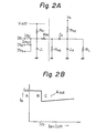
- Figure 2A shows a logic circuit which is used as an AND circuit according to the present invention
- Fig. 2B shows the condition for setting the threshold value in the circuit shown in Fig. 2A.
- the threshold value I th of the input signal current I in is made large, and the input signals I in1 and I in2 are injected into the input terminals IN1 and IN 2 after the operational point A is set, as is shown in Fig. 2B, the relationship I in1 + I in2 > I th is obtained (as is shown point c in Fig. 2B), and the output voltage V out is obtained. If the input signal current is supplied to only the input terminal IN 1 or IN 2 , the relationship between I and I in remains at point B, shown in Fig. 2B, with the result that the output voltage V out cannot be obtained.
- an AND circuit is formed. Further, in Fig. 2A, when a third input terminal IN 3 is provided so as to supply the input signal current, a two-thirds majority logic circuit can be formed. In such an AND circuit, which is different than the conventional AND circuit formed from a conventional current inject-type logic circuit, separation of the input and the output is possible, and no combination with an OR circuit is necessary.
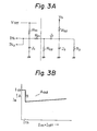
- Figure 3A shows a logic circuit used as an OR circuit according to the present invention
- Fig. 3B shows the condition for setting the threshold value.
- the value of the offset current I off is made large compared with the already mentioned AND circuit, and the threshold value (I th ) of the input signal current I in is made small.
- the output voltage V out can be obtained.
- an AND circuit, a majority circuit, or an OR circuit can be formed by setting the offset current of the input signal current.
- FIG. 4 shows the outline of the construction of such a circuit.
- the input terminal and the output terminal of each logic circuit are not shown, and 11 designates an AND circuit, 12 designates an OR circuit.
- OB designates an offset bus line, and BB designates a bias bus line.
- the input circuit portion A in Fig. 1A can be combined not only with the Josephson output logic circuit portion B in Fig. lA but also with any other Josephson logic circuit, with the result that the threshold value of such a logic circuit can be set in a suitable condition. That is, the logic circuit may be formed, beside aforementioned JAWS, other wellknown circuits, such as 4JL, DCL (Direct Conpled logic) or RCJL (Resistor Coupled Josephson Logic).
- DCL is disclosed, for example, in the article "Josephson-logic device circuits.
- DCI Device--coupled isolation
- RCJL is disclosed, for example, in the article “Resistor coupled Josephson logic” in "Applied Physics Letters” 40(8), 15 April 1982, pp. 741 to 744.
- an AND circuit which can separate the input and the output and which has an input signal level independent of the bias current level and an OR circuit which has a high gain can be constructed from one circuit. Therefore, when a Josephson integrated circuit is formed with such an AND circuit and such an OR circuit, the Josephson circuit is very effective.
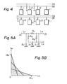
- Fig. 5A is a conventional Josephson logic AND circuit
- Fig. 5B is a diagram explaining the operation of the circuit shown in Fig. 5A.
- JA, JB, and JC are Josephson elements
- R 11 to R 13 are resistors
- LA and LB are input signal lines
- LO is an output signal line.
- the threshold characteristic of the AND circuit is as is shown in Fig. 5B.
- IA is a current which is input into the input signal line LA
- IA 0 is a critical current
- IB is a current which is input into the input signal line LB
- IB 0 is a critical current
- the output cannot appear inside the hatched portion shown in Fig. 5B.
- the output appears outside of the hatched portion. Therefore, for example, when the input is applied to the input signal line LA but is not applied to the input signal line LB, the output does not appear. Even in the opposite case, the output does not appear.
- the output appears when both input signal lines LA and LB receive the input, and thereby the AND operation is carried out.
- junction area in the Josephson element is set by the design, and the value of the critical current is determined by the set of such junction area. Therefore, the decrease of the critical currents IA O and IB O in the Josephson element is limited.
- the AND circuit can be operated on a small output of the OR circuit connected to the previous stage of the AND circuit, then a plurality of logic circuits can be operated on the full output of the OR circuit.
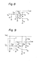
- Figure 6A is a circuit diagram illustrating an essential portion of an embodiment of the present invention
- Fig. 6B is a diagram illustrating the threshold characteristics of the embodiment shown in Fig. 6A.
- R 14 to R 17 are resistors J A , J B , and J C are Josephson elements (first, second, and third Josephson elements), Lout is an output signal line, L in1 and L in2 are a first input signal line and a second input signal line, respectively, Vs is a constant supply voltage for the circuit, I off is an offset current, I a and I b are input signal currents, and I 01 and I 02 are critical currents of the Josephson elements J A , J B , and J C .
- resistors R 14 and R 15 are constant current resistors and resistors R 16 and R 17 are separation resistors.
- the Josephson element J B is switched to a non-zero voltage state and the current I off + I b flows into the Josephson element J C .
- the Josephson element J C is not switched, with the result that no output appears on the output signal line L out . (the area II in Fig. 6B).
- the line which separates the hatched portion and the non-hatched portion in Fig. 6B is the threshold characteristics curve.
- the threshold level of the AND gate it is very easy to decrease the threshold level of the AND gate.
- the current I off may be increased, and the current I off may be adjusted at will because it is supplied from the exterior. It should be understood that the other critical currents may be dealt with in the same manner.
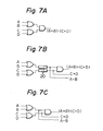
- Figure 7A is a block diagram illustrating the connection between conventional OR circuits and an AND circuit.
- A, B, C, and D designate input signals.
- the outputs of the OR circuits must be amplified with a current amplifier 20 shown in Fig. 7B.
- Figure 7C is a block diagram illustrating the connection between OR circuits and an AND circuit which is an embodiment of the present invention.
- the AND operation can be carried out with a small current level. Further, since the offset current flows to the output line, the output level of the AND circuit becomes large, with the result that the logic circuit connected to the next stage of the AND circuit can be sufficiently driven. Therefore, as is shown in Fig. 7C, the number of fan-outs of the OR circuits connected to previous stage of the AND circuit can be increased.
- Figure 8 is a conventional two-thirds majority logical circuit which was reported in the Appl. Phys. Lett., Vol. 40, No. 8, 15 April 1982 P. 741 ⁇ 744.
- J a , J b , J c , and J d designate Josephson elements
- R 21 , R 22 , R 23 , and R 24 designate resistors
- I A , I B , and I C designate input currents
- I out designates an output current.
- This circuit has a wide operation region. However, since all of the output currents of the logic circuits connected to the previous stage of the circuit must be injected into the circuit as the input currents I A , I B , and I C , the number of fan-outs in the previous stage is limited to one.
- Figure 9 is a circuit in which the drawback of the circuit shown in Fig. 8 is eliminated.
- the circuit is the same as the circuit shown in Fig. 6A.
- a two-thirds majority logic circuit which has a high input sensitivity, due to an offset current being supplied thereto, can be obtained.
- this circuit has a symmetry with respect to I A , I B , and I C , with the result that this circuit operates as an AND circuit for I A and I B , I B and I C , and I C and I A . That is, the logic equation of this circuit can be expressed as a two-thirds majority logical operation:
- This circuit has a characteristic which is substantially the same as that of the AND circuit shown in Fig. 6A.
- the Josephson logic circuit can be driven by a small current level, and, therefore, the charge of the logic gate connected to the previous stage can be decreased with the result that the number of used elements can be decreased, as can the operation time and the occupied area.
Landscapes
- Engineering & Computer Science (AREA)
- Power Engineering (AREA)
- Physics & Mathematics (AREA)
- Computer Hardware Design (AREA)
- Computing Systems (AREA)
- General Engineering & Computer Science (AREA)
- Mathematical Physics (AREA)
- Logic Circuits (AREA)
- Superconductor Devices And Manufacturing Methods Thereof (AREA)
Applications Claiming Priority (4)
| Application Number | Priority Date | Filing Date | Title |
|---|---|---|---|
| JP92802/82 | 1982-05-31 | ||
| JP9280282A JPS58209229A (ja) | 1982-05-31 | 1982-05-31 | ジヨセフソン論理回路 |
| JP229707/82 | 1982-12-28 | ||
| JP22970782A JPS59122235A (ja) | 1982-12-28 | 1982-12-28 | ジヨセフソン論理積回路 |
Publications (3)
| Publication Number | Publication Date |
|---|---|
| EP0095979A2 true EP0095979A2 (de) | 1983-12-07 |
| EP0095979A3 EP0095979A3 (en) | 1984-04-25 |
| EP0095979B1 EP0095979B1 (de) | 1986-10-29 |
Family
ID=26434181
Family Applications (1)
| Application Number | Title | Priority Date | Filing Date |
|---|---|---|---|
| EP83401069A Expired EP0095979B1 (de) | 1982-05-31 | 1983-05-27 | Josephson logische Schaltung |
Country Status (3)
| Country | Link |
|---|---|
| US (1) | US5455519A (de) |
| EP (1) | EP0095979B1 (de) |
| DE (1) | DE3367310D1 (de) |
Cited By (3)
| Publication number | Priority date | Publication date | Assignee | Title |
|---|---|---|---|---|
| US5170080A (en) * | 1991-08-14 | 1992-12-08 | Westinghouse Electric Corp. | Superconducting push-pull flux quantum digital logic circuits |
| EP0527557A1 (de) * | 1991-07-15 | 1993-02-17 | Hewlett-Packard Company | Schaltkreise und Methoden für beliebige Signale unter Verwendung von superleitenden Elementen |
| US5233243A (en) * | 1991-08-14 | 1993-08-03 | Westinghouse Electric Corp. | Superconducting push-pull flux quantum logic circuits |
Families Citing this family (27)
| Publication number | Priority date | Publication date | Assignee | Title |
|---|---|---|---|---|
| SE512591C2 (sv) * | 1995-06-30 | 2000-04-10 | Ericsson Telefon Ab L M | Anordning och förfarande avseende digital information |
| US6507234B1 (en) * | 2000-11-13 | 2003-01-14 | Trw Inc. | Active timing arbitration in superconductor digital circuits |
| US8571614B1 (en) | 2009-10-12 | 2013-10-29 | Hypres, Inc. | Low-power biasing networks for superconducting integrated circuits |
| WO2014197047A2 (en) | 2013-03-11 | 2014-12-11 | Massachusetts Institute Of Technology | Superconducting three-terminal device and logic gates |
| WO2016171875A1 (en) | 2015-04-03 | 2016-10-27 | Massachusetts Institute Of Technology | Current crowding in three-terminal superconducting devices and related methods |
| US10222416B1 (en) | 2015-04-14 | 2019-03-05 | Hypres, Inc. | System and method for array diagnostics in superconducting integrated circuit |
| WO2019160573A2 (en) | 2017-05-16 | 2019-08-22 | PsiQuantum Corp. | Superconducting signal amplifier |
| WO2019160572A2 (en) | 2017-05-16 | 2019-08-22 | PsiQuantum Corp. | Gated superconducting photon detector |
| WO2018232332A1 (en) | 2017-06-15 | 2018-12-20 | PsiQuantum Corp. | Niobium-germanium superconducting photon detector |
| US10586910B2 (en) | 2017-07-28 | 2020-03-10 | PsiQuantum Corp. | Superconductor-based transistor |
| US10374611B2 (en) | 2017-10-05 | 2019-08-06 | PsiQuantum Corp. | Superconducting logic components |
| US10461445B2 (en) | 2017-11-13 | 2019-10-29 | PsiQuantum Corp. | Methods and devices for impedance multiplication |
| US11200947B2 (en) | 2018-02-05 | 2021-12-14 | Massachusetts Institute Of Technology | Superconducting nanowire-based programmable processor |
| WO2019157077A1 (en) | 2018-02-06 | 2019-08-15 | PsiQuantum Corp. | Superconducting photon detector |
| US10972104B2 (en) | 2018-02-14 | 2021-04-06 | PsiQuantum Corp. | Superconducting logic components |
| WO2019213147A1 (en) | 2018-05-01 | 2019-11-07 | PsiQuantum Corp. | Photon number resolving superconducting detector |
| US10984857B2 (en) | 2018-08-16 | 2021-04-20 | PsiQuantum Corp. | Superconductive memory cells and devices |
| US10573800B1 (en) | 2018-08-21 | 2020-02-25 | PsiQuantum Corp. | Superconductor-to-insulator devices |
| US11101215B2 (en) | 2018-09-19 | 2021-08-24 | PsiQuantum Corp. | Tapered connectors for superconductor circuits |
| US11719653B1 (en) | 2018-09-21 | 2023-08-08 | PsiQuantum Corp. | Methods and systems for manufacturing superconductor devices |
| US10944403B2 (en) | 2018-10-27 | 2021-03-09 | PsiQuantum Corp. | Superconducting field-programmable gate array |
| US11289590B1 (en) | 2019-01-30 | 2022-03-29 | PsiQuantum Corp. | Thermal diode switch |
| US11569816B1 (en) | 2019-04-10 | 2023-01-31 | PsiQuantum Corp. | Superconducting switch |
| US11009387B2 (en) | 2019-04-16 | 2021-05-18 | PsiQuantum Corp. | Superconducting nanowire single photon detector and method of fabrication thereof |
| US11380731B1 (en) | 2019-09-26 | 2022-07-05 | PsiQuantum Corp. | Superconducting device with asymmetric impedance |
| US11585695B1 (en) | 2019-10-21 | 2023-02-21 | PsiQuantum Corp. | Self-triaging photon detector |
| US11994426B1 (en) | 2019-11-13 | 2024-05-28 | PsiQuantum Corp. | Scalable photon number resolving photon detector |
Family Cites Families (6)
| Publication number | Priority date | Publication date | Assignee | Title |
|---|---|---|---|---|
| US4117354A (en) * | 1977-06-30 | 1978-09-26 | International Business Machines Corporation | Two-part current injection interferometer amplifiers and logic circuits |
| US4313066A (en) * | 1979-08-20 | 1982-01-26 | International Business Machines Corporation | Direct coupled nonlinear injection Josephson logic circuits |
| JPS6010451B2 (ja) * | 1979-08-27 | 1985-03-18 | 工業技術院長 | ジヨゼフソン効果を利用したスイツチング回路 |
| US4482821A (en) * | 1980-06-10 | 1984-11-13 | Nippon Telegraph & Telephone Public Corporation | Superconductive logic circuit |
| US4413196A (en) * | 1981-08-31 | 1983-11-01 | Sperry Corporation | Three Josephson junction direct coupled isolation circuit |
| US4458160A (en) * | 1981-11-19 | 1984-07-03 | Sperry Corporation | High gain Josephson junction voltage amplifier |
-
1983
- 1983-05-27 DE DE8383401069T patent/DE3367310D1/de not_active Expired
- 1983-05-27 EP EP83401069A patent/EP0095979B1/de not_active Expired
-
1987
- 1987-03-20 US US07/028,075 patent/US5455519A/en not_active Expired - Fee Related
Cited By (3)
| Publication number | Priority date | Publication date | Assignee | Title |
|---|---|---|---|---|
| EP0527557A1 (de) * | 1991-07-15 | 1993-02-17 | Hewlett-Packard Company | Schaltkreise und Methoden für beliebige Signale unter Verwendung von superleitenden Elementen |
| US5170080A (en) * | 1991-08-14 | 1992-12-08 | Westinghouse Electric Corp. | Superconducting push-pull flux quantum digital logic circuits |
| US5233243A (en) * | 1991-08-14 | 1993-08-03 | Westinghouse Electric Corp. | Superconducting push-pull flux quantum logic circuits |
Also Published As
| Publication number | Publication date |
|---|---|
| US5455519A (en) | 1995-10-03 |
| EP0095979B1 (de) | 1986-10-29 |
| EP0095979A3 (en) | 1984-04-25 |
| DE3367310D1 (en) | 1986-12-04 |
Similar Documents
| Publication | Publication Date | Title |
|---|---|---|
| EP0095979A2 (de) | Josephson logische Schaltung | |
| US6188236B1 (en) | Arrangement and method relating to digital information in superconducting circuits | |
| US4897564A (en) | BICMOS driver circuit for high density CMOS logic circuits | |
| EP0435452A2 (de) | Supraleitende logische Schaltung mit Hystereseverhalten | |
| US4980580A (en) | CMOS interconnection circuit | |
| EP0111262A2 (de) | Ausgangsmultiplexer mit einfacher Gatterverzögerung | |
| US5295093A (en) | Polarity-convertible Josephson driver circuit | |
| Gheewala et al. | Josephson direct coupled logic (DCL) | |
| EP0076160A2 (de) | Logische Schaltung mit Josephson-Verbindung | |
| EP0074666B1 (de) | Den Josephson-Effekt verwendende Schaltung | |
| US4672244A (en) | Josephson logic integrated circuit | |
| GB2078046A (en) | Superconductive logic circuit | |
| US4413197A (en) | Four Josephson junction direct-coupled and gate circuit | |
| US4835455A (en) | Reference voltage generator | |
| US4859879A (en) | Superconducting digital logic amplifier | |
| US4678945A (en) | Unidirectional single-flux-quantum logic circuit | |
| EP0361527A2 (de) | Logische Schaltung | |
| US4559459A (en) | High gain non-linear threshold input Josephson junction logic circuit | |
| EP0069534B1 (de) | Supra-leitende-logische Schaltung | |
| US4225854A (en) | High density analog-to-binary coded decimal converter | |
| JPH0659028B2 (ja) | 論理回路 | |
| JPS5840945U (ja) | 3ジヨセフソン接合直結形分離回路 | |
| US4538077A (en) | Circuit utilizing Josephson effect | |
| US4506172A (en) | Decoder circuit utilizing josephson devices | |
| EP0430653B1 (de) | ECL-Logikschaltung mit Diodenlast |
Legal Events
| Date | Code | Title | Description |
|---|---|---|---|
| PUAI | Public reference made under article 153(3) epc to a published international application that has entered the european phase |
Free format text: ORIGINAL CODE: 0009012 |
|
| AK | Designated contracting states |
Designated state(s): DE FR GB |
|
| PUAL | Search report despatched |
Free format text: ORIGINAL CODE: 0009013 |
|
| AK | Designated contracting states |
Designated state(s): DE FR GB |
|
| 17P | Request for examination filed |
Effective date: 19840707 |
|
| GRAA | (expected) grant |
Free format text: ORIGINAL CODE: 0009210 |
|
| AK | Designated contracting states |
Kind code of ref document: B1 Designated state(s): DE FR GB |
|
| REF | Corresponds to: |
Ref document number: 3367310 Country of ref document: DE Date of ref document: 19861204 |
|
| ET | Fr: translation filed | ||
| PLBE | No opposition filed within time limit |
Free format text: ORIGINAL CODE: 0009261 |
|
| STAA | Information on the status of an ep patent application or granted ep patent |
Free format text: STATUS: NO OPPOSITION FILED WITHIN TIME LIMIT |
|
| 26N | No opposition filed | ||
| PGFP | Annual fee paid to national office [announced via postgrant information from national office to epo] |
Ref country code: GB Payment date: 19900406 Year of fee payment: 8 |
|
| PGFP | Annual fee paid to national office [announced via postgrant information from national office to epo] |
Ref country code: FR Payment date: 19900531 Year of fee payment: 8 |
|
| PGFP | Annual fee paid to national office [announced via postgrant information from national office to epo] |
Ref country code: DE Payment date: 19900723 Year of fee payment: 8 |
|
| PG25 | Lapsed in a contracting state [announced via postgrant information from national office to epo] |
Ref country code: GB Effective date: 19910527 |
|
| GBPC | Gb: european patent ceased through non-payment of renewal fee | ||
| PG25 | Lapsed in a contracting state [announced via postgrant information from national office to epo] |
Ref country code: FR Effective date: 19920131 |
|
| PG25 | Lapsed in a contracting state [announced via postgrant information from national office to epo] |
Ref country code: DE Effective date: 19920303 |
|
| REG | Reference to a national code |
Ref country code: FR Ref legal event code: ST |