EP0095083B1 - Circuit d'acquisition de l'horloge d'un message binaire codé en NRZ - Google Patents
Circuit d'acquisition de l'horloge d'un message binaire codé en NRZ Download PDFInfo
- Publication number
- EP0095083B1 EP0095083B1 EP19830104577 EP83104577A EP0095083B1 EP 0095083 B1 EP0095083 B1 EP 0095083B1 EP 19830104577 EP19830104577 EP 19830104577 EP 83104577 A EP83104577 A EP 83104577A EP 0095083 B1 EP0095083 B1 EP 0095083B1
- Authority
- EP
- European Patent Office
- Prior art keywords
- clock
- message
- transitions
- shift register
- output
- Prior art date
- Legal status (The legal status is an assumption and is not a legal conclusion. Google has not performed a legal analysis and makes no representation as to the accuracy of the status listed.)
- Expired
Links
Images

Classifications
-
- H—ELECTRICITY
- H04—ELECTRIC COMMUNICATION TECHNIQUE
- H04L—TRANSMISSION OF DIGITAL INFORMATION, e.g. TELEGRAPHIC COMMUNICATION
- H04L7/00—Arrangements for synchronising receiver with transmitter
- H04L7/02—Speed or phase control by the received code signals, the signals containing no special synchronisation information
- H04L7/033—Speed or phase control by the received code signals, the signals containing no special synchronisation information using the transitions of the received signal to control the phase of the synchronising-signal-generating means, e.g. using a phase-locked loop
- H04L7/0331—Speed or phase control by the received code signals, the signals containing no special synchronisation information using the transitions of the received signal to control the phase of the synchronising-signal-generating means, e.g. using a phase-locked loop with a digital phase-locked loop [PLL] processing binary samples, e.g. add/subtract logic for correction of receiver clock
Definitions
- the present invention is in the field of digital transmissions and relates to the recovery of the clock defining the time intervals between which all the transitions of a binary message coded in NRZ lie.
- circuits for acquiring the clock of a binary message coded in NRZ comprise, as a general rule, a local clock, at the frequency of the clock of the binary message coded in expected NRZ, provided with a phase-locked loop tending to make the transitions of the binary message coincide with its beginnings of period.
- the loop is formed by a device for adjusting the phase of the local clock controlled by a comparator which detects the position of the transitions of the binary message coded in NRZ relative to the beginnings of the periods of the local clock. More or less sophisticated filters are inserted between the comparator and the phase adjustment device in order to obtain a very short acquisition time and a high insensitivity to interference.
- the clock acquisition capacity of a binary message is an important characteristic, in particular in the case where binary messages coded in NRZ are in the form of asynchronous trains and where any delay in clock acquisition can lead either data loss or the need to use a prohibitively large buffer.
- it is thwarted by the existence, for the phase control of the local clock, of an unstable equilibrium position which corresponds to a local clock in phase opposition with that of the message received and in which the slaving can be maintained for a certain time by a succession of alternating corrections of advance and of phase delay.
- the elimination of the unstable equilibrium position from their phase control results from a detection consisting in verifying that there does not exist, in the message received, of transition in the vicinity of the middle of the periods of the local clock and, if not, of a brutal correction of phase causing the release of the phase control from its position of false equilibrium.
- the aim of the present invention is to reduce the time for acquiring the clock of a message coded in NRZ by avoiding, at the start of an acquisition procedure, the possibility of reaching the false balance for the phase control of the local clock this, thanks to a preset of the phase of the local clock on a more or less rough preliminary estimate of the phase of the clock of the received message carried out while the latter transits in a delay line.
- It relates to a circuit for acquiring the clock of a binary message coded in NRZ comprising timing means generating a timing signal having a frequency equal to a multiple p of that of the clock of the binary message and defining successive time windows of the same duration, accounting means operating on the transitions of the signal received from several clock periods, maximum detection means operating on the accounts obtained, characterized in that the accounting means group together the time windows by classes as a function of their modulo p rank with respect to an arbitrary origin and determine during each time window the count of the transitions having coincided with previous windows of the same class modulo p as the current time window, and the detection means maximum deliver an initialization signal during the time windows belonging to the modulo p class having the co mpte maximum, the circuit further comprising a local clock at the clock frequency of the received message, synchronized at the start of an acquisition procedure by the maximum detection means.
- a circuit for acquiring the timing clock of a binary message coded in NRZ comprising timing means having a frequency equal to a multiple p of that of the clock of the binary message and defining windows successive temporal data of the same duration, census means operating on the transitions of the message received for several clock periods, minimum detection means operating on the differences in distribution obtained, characterized in that the census means group together the time windows by classes according to their rank modulo p with respect to an arbitrary origin and determine during each time window, the difference in distribution between the early and late transitions compared to time windows of the same class as the time window in progress, and the minimum detection means delivering a clock initialization signal during windows temporals belonging to the modulo p class having the smallest difference in distribution, the circuit further comprising doubt removal means inhibiting the minimum detection means when the difference in distribution for a time window class having a modulo p rank at the lower of -p / 2 or respectively at the most of p / 2 higher than the rank of the class of windows for which a minimum distribution
- the estimation of the modulo p rank of the class of time windows with which the beginnings of the periods of the clock of the received message coincide allows an initial setting of the local clock with a phase difference at most equal to 2 rr / p, the number p is chosen so that this difference is small enough to eliminate the possibility of convergence of a phase control towards the position of false equilibrium and even preferably to allow, with a good probability a correct processing of the data of the received message.
- the census means advantageously consist of accounting means supplemented by calculation means delivering the distribution difference relating to time windows of the same modulo p rank as the current time window by operating by recurrence from the distribution difference calculated at price of the previous time window and the most recent values previously obtained for the accounts relating to different classes of time windows.
- the circuit shown in Figure 1 has an input 1 to which the asynchronous binary messages are applied and several outputs 2, 3 and 4. We find on an output 2 the messages applied to input 1 after a constant delay including the time d acquisition of the phases of their clocks, on another output 3 a binary signal D of modulation detection representative of the actual presence or not of a binary message at output 2 and on another output 4 the clock signal recovered from binary message available at output 2.
- It essentially comprises a local clock 5 at the frequency F of the clocks of received messages slaved in phase on the transitions of the binary message available at output 2, a delay line 6 inserted between input 1 and the local clock 5 compensating for the phase acquisition time, and a rapid phase acquisition circuit 7 which ensures the detection of a modulation, the initial synchronization of the local clock 5 and, indirectly, control of its mode of control.
- the local clock 5 is provided with a first order phase control loop with two integrating filters 54, 55 switched via a selector 56.
- One of the filters 54 has a low time constant for allow the passage of the zero phase difference in ten bits of a message but sufficient to ensure the stability of the convergence of the phase control beyond the performance of the fast phase acquisition circuit 7.
- the another filter 55 has a large time constant to allow the maintenance of the acquired phase even in the event of momentary loss or suffocation of the link but compatible with a slip at least equal to twice that expected between transmission and reception.
- the low time constant filter 54 is in service in the absence of modulation detection and in the presence of modulation detection during the first bits of a message, the time to acquire a zero phase difference. It is then replaced by the other filter 55.
- the local clock 5 comprises, in a conventional manner, an oscillator 50 at a frequency F 'equal to an integer multiple r of the frequency F followed by a phase modulator produced with a divider by r 51 provided with a reset command to zero and a command allowing its division ratio to be modified by ⁇ 1.
- the reset command is used by the clock acquisition circuit 7 for the initial synchronization of the local clock.
- the command to modify the division ratio r by ⁇ 1 is used by the phase locked loop to cause, as necessary, a phase advance or delay of the local clock 5.
- the phase control loop of the local clock 5 comprises a transition detector 53 which receives as input the binary messages from the delay line 6 and delivers at its output pulses of short duration coinciding with the transitions of these messages .
- a phase comparator 54 with two inputs, one connected to the output of the programmable divider 51, the other to that of the transition detector 53, directs these pulses to one or other of its outputs A, R according to that they are late or in phase advance with respect to the transitions of a given direction of the local clock signal considered as the beginning of the period.
- the integration filters 54, 55 connected to the two outputs of the comparator deliver on a two-bit output a hold or correction signal in advance or behind the phase of the local clock signal so as to balance the number of pulses on the two outputs of the phase comparator 52.
- They are, for example, stochastic recurrence of the "N before M" type as described by JR CESSNA in an article published in the journal IEEE Transactions on Communications VOL. COM. 20 N ° 2, April 72, one with small N and M values giving it low inertia, the other with large N and M values giving it high inertia.
- the selector 56 activates one or other of the integration filters 54, 55. It can be controlled, as shown by means of a bistable 8 and a counter 9.
- the modulation detection signal D keeps the counter 9 at zero and the bistable in a so-called rest position corresponding to the selection of the integration filter 54 or 55 with low time constant.
- the counter 9 counts the bits of this message and, arrived at its maximum capacity, sends a switching pulse to the bistable 8 which changes state and selects the integration filter with a large time constant.
- the fast phase acquisition circuit 7 essentially comprises two parts, one 71 ensuring the detection of a modulation, that is to say the presence of a message in transit in the delay line 6 emitting a signal of modulation detection D and the other 72 ensuring clock acquisition, that is to say an estimation of the initial phase of the message in transit in the delay line 6.
- the modulation detection circuit 71 can comprise an autocorrelator with two inputs connected to the ends of the delay line 6 which calculates the autocorrelation value between two versions of the signal received in transit in the delay line 6 delayed one with respect to the other of a half clock period and a double threshold comparator generating a binary signal D passing to a state corresponding to a modulation detection when the autocorrelation value delivered by the autocorrelator is greater at a lower threshold below which it is considered that the received signal is noise and below a higher threshold above which it is considered that there is absence of received signal.
- the clock acquisition circuit 72 generates from the signals at the ends of the delay line 6, a binary clock initialization signal H, whose transitions from 0 to 1 approach the beginnings clock periods of a message in transit in the delay line 6 when such a message actually exists.
- This signal H is applied to a monostable 73 which sends reset pulses from the programmable divider 51 of the local clock 5 when it is not blocked by the signal D of the modulation detection circuit, ie only at the start of each modulation detection and for a single trigger.
- the initial estimation of the clock phase of the received message is done by dividing the duration of a clock period into p successive time windows of the same duration, by grouping these windows by classes according to their rank modulo p with respect to to an arbitrary origin chosen locally and by determining the class of windows most often coinciding with the transitions of the message received and stored in the delay line 6. This determination can be done simply by counting, during each time window, the number of transitions of the message stored in the delay line 6 having coincided with previous time windows of the same class modulo p and detecting whether this number is maximum.
- FIG. 2 illustrates the diagram of a clock acquisition circuit operating in this way. It has, in addition to its inputs 100, 101 by which it receives the signals present at the ends of the delay line 6, a timing input 102 on which it receives a timing signal H, defining the width of the time windows, having p times the frequency F and which can be obtained from the oscillator 50 of the local clock by an adequate ratio division.
- Two transition detectors 103, 104 are connected to the ends of the delay line 6 and output pulses of the same width as a time window, synchronous with the transitions.
- a p-stage shift register 105 punctuated by the timing signal H plays the role of a circulating memory which stores the accounts of the transitions of the signal contained in the delay line 6 having occurred in the p classes of time windows .
- An adder 106 looped on itself via the shift register 105 ensures the updating of the various accounts.
- it has a unit increment input which is connected to the output of the transition detector 103 connected to the input of the delay line 6 and which allows the consideration of each newly received transition, and a decrementing input of a unit which is connected to the output of the transition detector 104 connected to the output of the delay line 6 and which allows the counting of each transition of the signal leaving the delay line 6.
- a relative maximum detector outputs a binary signal at logic level 1 if the account of the modulo p class to which the current time window belongs is greater than the accounts of the modulo p classes of the time windows immediately preceding and following the time window in Classes. It consists of two comparators 107, 108 with two inputs connected one to the input and output of the first stage of the shift register 105 and the other to the input of the shift register 105 and the output of its top floor, and a logic gate of type "and" 109.
- a threshold comparator 110 connected to the output of the adder 106 blocks the output of the detector relative maximum by means of a logic gate of type "and" 111 in the case where the detected maximum does not exceed a certain threshold chosen as a function of the noise which may affect the message received.
- the detection of the modulo p class of time windows coinciding with the majority of the transitions of the message stored in the delay line 6 can also be done from the determination among the modulo p classes of time windows, of that with respect to the windows of which message transitions are most evenly distributed on both sides.
- This determination is less sensitive to noise because it makes it possible to implement for each class most of the transitions of the message stored in the delay line 6 and not only those coinciding with the time windows of the class considered.
- it has the disadvantage of leading to uncertainty, the transitions being distributed in a balanced manner both on both sides of the class of windows with which they coincide for the most part and on both sides of the class of time windows with which they are mostly phase shifted by half a clock period.
- the advance domain coincides with the time windows whose classes have a modulo p rank less than the ith by at most p / 2 while the delay domain coincides with the time windows whose classes have a modulo p rank greater than the ith at most p / 2.
- the class of windows of rank i must be excluded from or included therein according to whether the number p of time windows per clock period is odd or even.
- the transitions of the message in transit in the delay line 6 in advance with respect to the time windows of the class of rank i are those which coincided with time windows belonging to classes of rank j verifying conditions: while the backward transitions compared to the time windows of the class of rank i are those which coincided with time windows belonging to classes of rank j satisfying the conditions:
- the difference in distribution y between the early and late phase transitions with respect to the time windows of the ith class is expressed as a function of the numbers x ; of transitions coinciding with the time windows of a row j by the expression: and can take the form: which brings up the expression of the difference in distribution Yi - J.
- the indices are to be considered modulo p: we get the recurrence formula:
- the number p of time windows per clock period is an even integer, it is necessary to include the windows of the class of rank i considered in one of the domains of advance or delay which amounts to taking as benchmarks of early or late for the transitions of the message the beginnings or the ends of the windows of the class of rank i. If the windows of this last class are put in the delay domain the recurrence formula becomes: while otherwise it becomes:
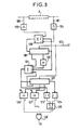
- FIG. 3 illustrates the diagram of a clock acquisition circuit which is adapted to the case of an odd number p of time windows per clock period and which implements the recurrence relation (1).
- This circuit comprises, like that of FIG. 2, two inputs 100, 101 connected to the ends. of the delay line 6 and an input 102 receiving a timing signal H 1 which defines the width of the time windows and whose frequency is an odd multiple p of the frequency F obtained from the oscillator 50 by a ratio division adequate, a p-stage shift register 105 punctuated by the timing signal H 1 playing the role of a circulating memory memorizing the accounts x, transitions of the message contained in the delay line 6 having occurred in the different classes modulo p of time windows, an adder 106 looped in on itself by means of the shift register with p stages 105 ensuring the updating of the accounts thanks to an increment input of a unit connected via a transition detector 103 at the input of the delay line 6 and at a decrementing input of a unit connected via a transition detector 104 at the output of the delay line 6.
- a second shift register 102 with p stages- punctuated by the timing signal H 1 plays the role of a circulating memory preserving over a duration of a clock period the differences in distribution y calculated during p time windows previously elapsed.
- An adder 121 looped on itself through the first stage of the shift register 120 performs the calculation of the distribution difference y between the transitions of the message in transit in the delay line 6 in advance and respectively in delay with respect to the class of time windows to which the current time window belongs.
- the class modulo p of the time windows with respect to which the transitions of the message contained in the delay line 6 are distributed on both sides in the most equitable manner is that for which the difference in distribution there is minimum in absolute value .
- the search for this minimum is done by means of two extractor circuits of absolute value 123, 124 and of a comparator 125 with two inputs connected to their suite.
- the absolute value extractor circuit 123 is connected at the input to the output of the adder 121 where the distribution difference y relative to the class in modulo y of the current window is available, while the absolute value extractor circuit 124 is connected at the input to the output of the last stage of the shift register 120 where the distribution difference y i + 1 relating to the modulo p class of the time window which will follow that in progress is available.
- Comparator 125 outputs a binary signal in logic state 1 as long as the distribution difference y relative to the modulo p class of the current window is less in absolute value than that y i + 1 of the modulo p class of the time window that will follow.
- Two threshold comparators 126, 127 control the output of the comparator 125 via a logic gate of type "and" 128 delivering a clock initialization signal H I. Their function is to remove the doubt mentioned above.
- One 126 of the threshold comparators is connected at the input to the output of a stage of the shift register 120 whose rank is close to (p-1) and outputs a binary signal at logic state 1 if the difference in distribution y which it receives from the shift register 120 is negative.
- the other threshold comparator 127 is connected to the output of a stage of the shift register 120 whose rank is close to (3 p-1) and outputs a binary signal at logic state 1 if the difference in distribution y which it receives from the shift register 120 is positive.
- the difference there is at the output of the shift register 120 of rank close to relates to a class of time windows having a rank lower than the rank i of the current time window by approximately (p-1) and consequently preceding the time windows of rank i by approximately a quarter of a clock period.
- the difference in distribution y passes through a minimum in absolute value for the time windows of rank i, it is necessarily negative if these windows coincide with the majority of the transitions of the message, and necessarily positive if these windows are phase shifted by half clock period compared to the majority of message transitions. This state of affairs is used by the threshold comparator 126 to eliminate the detection of the absolute minimum corresponding to the false balance.
- the difference in distribution there at the output of the shift register 120 of rank close to (3p-1) relates to a class of time windows having a rank lower than rank i of the current time window of approximately (3p-1) or, taking into account the definition of ranks modulo p, having a rank greater than rank i of the current time window by about and consequently following the time windows of rank i of about a quarter of a clock period.
- the difference in distribution y passes through a minimum in absolute value for the time windows of rank i, it is necessarily positive if these windows are phase shifted by a half clock period with respect to the majority of the transitions of the message. This state of affairs is used by the threshold comparator 127 to eliminate the detection of the absolute minimum corresponding to the false balance.
- the clock initialization signal H i has transitions from 0 to 1 which only appear during time windows coinciding with the beginnings of the message clock periods and which are used for the initial synchronization of the local clock 5.
- the adder 121 is advantageously a digital circuit calculating in binary complement to two which gives a structure of great simplicity to the comparators with thresholds 126, 127 which have only 'to transmit or reverse the sign bit and to the extractor circuits of absolute value 123,124 which only have to eliminate the sign bit.
Applications Claiming Priority (2)
| Application Number | Priority Date | Filing Date | Title |
|---|---|---|---|
| FR8208546 | 1982-05-17 | ||
| FR8208546A FR2527031A1 (fr) | 1982-05-17 | 1982-05-17 | Circuit d'acquisition de l'horloge d'un message binaire code en nrz |
Publications (2)
| Publication Number | Publication Date |
|---|---|
| EP0095083A1 EP0095083A1 (fr) | 1983-11-30 |
| EP0095083B1 true EP0095083B1 (fr) | 1987-01-28 |
Family
ID=9274096
Family Applications (1)
| Application Number | Title | Priority Date | Filing Date |
|---|---|---|---|
| EP19830104577 Expired EP0095083B1 (fr) | 1982-05-17 | 1983-05-10 | Circuit d'acquisition de l'horloge d'un message binaire codé en NRZ |
Country Status (6)
| Country | Link |
|---|---|
| EP (1) | EP0095083B1 (xx) |
| DE (1) | DE3369620D1 (xx) |
| DK (1) | DK160171C (xx) |
| FR (1) | FR2527031A1 (xx) |
| GR (1) | GR78569B (xx) |
| IE (1) | IE54411B1 (xx) |
Families Citing this family (1)
| Publication number | Priority date | Publication date | Assignee | Title |
|---|---|---|---|---|
| US4972444A (en) * | 1988-07-14 | 1990-11-20 | International Business Machines Corporation | Digital phase-locked device and method |
Family Cites Families (3)
| Publication number | Priority date | Publication date | Assignee | Title |
|---|---|---|---|---|
| US3851101A (en) * | 1974-03-04 | 1974-11-26 | Motorola Inc | Adaptive phase synchronizer |
| FR2283592A1 (fr) * | 1974-08-27 | 1976-03-26 | Thomson Csf | Dispositif extracteur de synchronisation et systeme de transmission d'informations comportant un tel dispositif |
| FR2458181A1 (fr) * | 1979-06-01 | 1980-12-26 | Thomson Csf | Dispositif de synchronisation d'un signal d'horloge et systemes de transmission de donnees synchrones comportant un tel dispositif |
-
1982
- 1982-05-17 FR FR8208546A patent/FR2527031A1/fr active Granted
-
1983
- 1983-05-10 DE DE8383104577T patent/DE3369620D1/de not_active Expired
- 1983-05-10 EP EP19830104577 patent/EP0095083B1/fr not_active Expired
- 1983-05-16 IE IE113583A patent/IE54411B1/en not_active IP Right Cessation
- 1983-05-16 DK DK217383A patent/DK160171C/da not_active IP Right Cessation
- 1983-05-17 GR GR71372A patent/GR78569B/el unknown
Also Published As
| Publication number | Publication date |
|---|---|
| EP0095083A1 (fr) | 1983-11-30 |
| FR2527031A1 (fr) | 1983-11-18 |
| IE831135L (en) | 1983-11-17 |
| DE3369620D1 (en) | 1987-03-05 |
| IE54411B1 (en) | 1989-09-27 |
| DK160171B (da) | 1991-02-04 |
| DK160171C (da) | 1991-07-01 |
| DK217383A (da) | 1983-11-18 |
| DK217383D0 (da) | 1983-05-16 |
| GR78569B (xx) | 1984-09-27 |
| FR2527031B1 (xx) | 1984-12-07 |
Similar Documents
| Publication | Publication Date | Title |
|---|---|---|
| EP0419337B1 (fr) | Procédé de codage d'un signal numérique, codeur et décodeur pour la mise en oeuvre de ce procédé, procédé de régénération et régénérateur correspondant | |
| EP0013990B1 (fr) | Procédé de transmission série d'informations binaires et dispositifs pour sa mise en oeuvre | |
| FR2498032A1 (fr) | Synchroniseur de bits pour signaux numeriques | |
| EP0013343B1 (fr) | Procédé et dispositif pour détecter une séquence pseudo-aléatoire de changements de phase de 0 degré et 180 degrés de la porteuse dans un récepteur de données | |
| EP0023852B1 (fr) | Procédé et dispositif pour la mise en phase d'une horloge locale | |
| EP0730377B1 (fr) | Traitement d'un signal asynchrone présentant periodiquement des salves de synchronisation | |
| EP0400520B1 (fr) | Dispositif de détection de perte de signal de réception pour récepteur de signaux numériques | |
| EP0012880B1 (fr) | Procédé de décodage de données binaires codées en phase, modulation de fréquence et modulation de fréquence modifiée | |
| FR2615677A1 (fr) | Circuit de boucle de verrouillage de phase numerique | |
| EP0095083B1 (fr) | Circuit d'acquisition de l'horloge d'un message binaire codé en NRZ | |
| EP1101316B1 (fr) | Procede de recuperation d'horloge lors de l'echantillonnage de signaux de type numerique | |
| FR2764147A1 (fr) | Procede et dispositif de recuperation de synchronisation sur un signal transmis a un recepteur de telephone mobile | |
| EP0056208A1 (fr) | Procédé et dispositif de synchronisation de messages | |
| EP0647018A1 (fr) | Comparateur de phase numérique | |
| EP0109658A1 (fr) | Equipement de transmission synchrone de données | |
| FR2646742A1 (fr) | Dispositif pour synchroniser un signal pseudo-binaire avec un signal d'horloge regeneree a sauts de phase | |
| FR2799852A1 (fr) | Procede et dispositif d'extraction de donnees binaires vehiculees par un signal incident, en particulier un signal issu d'un disque numerique | |
| EP0526359A1 (fr) | Procédé et dispositif de synchronisation d'un signal | |
| EP0905946B1 (fr) | Commande d'échantillonnage d'un signal biphase | |
| EP0045260B1 (fr) | Démodulateur de signaux modulés suivant une modulation de phase continue et système de transmission comportant un tel démodulateur | |
| FR2623675A1 (fr) | Dispositif de synchronisation d'une horloge par rapport a un signal numerique incident, notamment a haut debit | |
| FR2816075A1 (fr) | Generateur ameliore pour la production de signaux d'horloge | |
| EP0092879A2 (fr) | Dispositif de synchronisation bit pour modulateur-démodulateur ou récepteur de transmission de données | |
| EP0368417B1 (fr) | Appareil muni d'un dispositif de restitution de la composante continue amélioré | |
| FR3071982B1 (fr) | Module de controle de compatibilite electromagnetique au sein d'un signal cdma recu par un recepteur de donnee(s) cdma |
Legal Events
| Date | Code | Title | Description |
|---|---|---|---|
| PUAI | Public reference made under article 153(3) epc to a published international application that has entered the european phase |
Free format text: ORIGINAL CODE: 0009012 |
|
| AK | Designated contracting states |
Designated state(s): BE DE FR GB IT LU NL |
|
| 17P | Request for examination filed |
Effective date: 19840524 |
|
| GRAA | (expected) grant |
Free format text: ORIGINAL CODE: 0009210 |
|
| AK | Designated contracting states |
Kind code of ref document: B1 Designated state(s): BE DE FR GB IT LU NL |
|
| ITF | It: translation for a ep patent filed |
Owner name: JACOBACCI & PERANI S.P.A. |
|
| REF | Corresponds to: |
Ref document number: 3369620 Country of ref document: DE Date of ref document: 19870305 |
|
| PLBE | No opposition filed within time limit |
Free format text: ORIGINAL CODE: 0009261 |
|
| STAA | Information on the status of an ep patent application or granted ep patent |
Free format text: STATUS: NO OPPOSITION FILED WITHIN TIME LIMIT |
|
| 26N | No opposition filed | ||
| PGFP | Annual fee paid to national office [announced via postgrant information from national office to epo] |
Ref country code: GB Payment date: 19920427 Year of fee payment: 10 |
|
| PGFP | Annual fee paid to national office [announced via postgrant information from national office to epo] |
Ref country code: DE Payment date: 19920502 Year of fee payment: 10 |
|
| PGFP | Annual fee paid to national office [announced via postgrant information from national office to epo] |
Ref country code: LU Payment date: 19920513 Year of fee payment: 10 |
|
| PGFP | Annual fee paid to national office [announced via postgrant information from national office to epo] |
Ref country code: BE Payment date: 19920518 Year of fee payment: 10 |
|
| PGFP | Annual fee paid to national office [announced via postgrant information from national office to epo] |
Ref country code: FR Payment date: 19920521 Year of fee payment: 10 |
|
| ITTA | It: last paid annual fee | ||
| PGFP | Annual fee paid to national office [announced via postgrant information from national office to epo] |
Ref country code: NL Payment date: 19920531 Year of fee payment: 10 |
|
| EPTA | Lu: last paid annual fee | ||
| PG25 | Lapsed in a contracting state [announced via postgrant information from national office to epo] |
Ref country code: LU Free format text: LAPSE BECAUSE OF NON-PAYMENT OF DUE FEES Effective date: 19930510 Ref country code: GB Effective date: 19930510 |
|
| PG25 | Lapsed in a contracting state [announced via postgrant information from national office to epo] |
Ref country code: BE Effective date: 19930531 |
|
| BERE | Be: lapsed |
Owner name: SINTRA-ALCATEL Effective date: 19930531 |
|
| PG25 | Lapsed in a contracting state [announced via postgrant information from national office to epo] |
Ref country code: NL Effective date: 19931201 |
|
| GBPC | Gb: european patent ceased through non-payment of renewal fee |
Effective date: 19930510 |
|
| NLV4 | Nl: lapsed or anulled due to non-payment of the annual fee | ||
| PG25 | Lapsed in a contracting state [announced via postgrant information from national office to epo] |
Ref country code: FR Effective date: 19940131 |
|
| PG25 | Lapsed in a contracting state [announced via postgrant information from national office to epo] |
Ref country code: DE Effective date: 19940201 |
|
| REG | Reference to a national code |
Ref country code: FR Ref legal event code: ST |