EP0093902A1 - Power supply with load-transient anticipation - Google Patents
Power supply with load-transient anticipation Download PDFInfo
- Publication number
- EP0093902A1 EP0093902A1 EP83103806A EP83103806A EP0093902A1 EP 0093902 A1 EP0093902 A1 EP 0093902A1 EP 83103806 A EP83103806 A EP 83103806A EP 83103806 A EP83103806 A EP 83103806A EP 0093902 A1 EP0093902 A1 EP 0093902A1
- Authority
- EP
- European Patent Office
- Prior art keywords
- power supply
- load
- load device
- power
- reaction
- Prior art date
- Legal status (The legal status is an assumption and is not a legal conclusion. Google has not performed a legal analysis and makes no representation as to the accuracy of the status listed.)
- Granted
Links
- 230000008859 change Effects 0.000 claims abstract description 13
- 238000000034 method Methods 0.000 claims description 7
- 230000009471 action Effects 0.000 claims description 3
- 230000000694 effects Effects 0.000 claims description 3
- 238000005070 sampling Methods 0.000 claims 6
- 230000004044 response Effects 0.000 abstract description 5
- 230000003466 anti-cipated effect Effects 0.000 abstract description 3
- 230000001105 regulatory effect Effects 0.000 description 7
- 230000001052 transient effect Effects 0.000 description 6
- 230000015654 memory Effects 0.000 description 5
- 239000003990 capacitor Substances 0.000 description 4
- 238000012937 correction Methods 0.000 description 4
- 230000033228 biological regulation Effects 0.000 description 3
- 238000010586 diagram Methods 0.000 description 3
- 238000011068 loading method Methods 0.000 description 3
- 230000003247 decreasing effect Effects 0.000 description 2
- 230000001939 inductive effect Effects 0.000 description 2
- 230000000630 rising effect Effects 0.000 description 2
- 230000007704 transition Effects 0.000 description 2
- 230000004913 activation Effects 0.000 description 1
- 230000001276 controlling effect Effects 0.000 description 1
- 230000009849 deactivation Effects 0.000 description 1
- 230000006870 function Effects 0.000 description 1
- 230000002093 peripheral effect Effects 0.000 description 1
- 230000001629 suppression Effects 0.000 description 1
Images

Classifications
-
- H—ELECTRICITY
- H02—GENERATION; CONVERSION OR DISTRIBUTION OF ELECTRIC POWER
- H02M—APPARATUS FOR CONVERSION BETWEEN AC AND AC, BETWEEN AC AND DC, OR BETWEEN DC AND DC, AND FOR USE WITH MAINS OR SIMILAR POWER SUPPLY SYSTEMS; CONVERSION OF DC OR AC INPUT POWER INTO SURGE OUTPUT POWER; CONTROL OR REGULATION THEREOF
- H02M3/00—Conversion of dc power input into dc power output
- H02M3/22—Conversion of dc power input into dc power output with intermediate conversion into ac
- H02M3/24—Conversion of dc power input into dc power output with intermediate conversion into ac by static converters
- H02M3/28—Conversion of dc power input into dc power output with intermediate conversion into ac by static converters using discharge tubes with control electrode or semiconductor devices with control electrode to produce the intermediate ac
- H02M3/325—Conversion of dc power input into dc power output with intermediate conversion into ac by static converters using discharge tubes with control electrode or semiconductor devices with control electrode to produce the intermediate ac using devices of a triode or a transistor type requiring continuous application of a control signal
- H02M3/335—Conversion of dc power input into dc power output with intermediate conversion into ac by static converters using discharge tubes with control electrode or semiconductor devices with control electrode to produce the intermediate ac using devices of a triode or a transistor type requiring continuous application of a control signal using semiconductor devices only
- H02M3/33507—Conversion of dc power input into dc power output with intermediate conversion into ac by static converters using discharge tubes with control electrode or semiconductor devices with control electrode to produce the intermediate ac using devices of a triode or a transistor type requiring continuous application of a control signal using semiconductor devices only with automatic control of the output voltage or current, e.g. flyback converters
- H02M3/33515—Conversion of dc power input into dc power output with intermediate conversion into ac by static converters using discharge tubes with control electrode or semiconductor devices with control electrode to produce the intermediate ac using devices of a triode or a transistor type requiring continuous application of a control signal using semiconductor devices only with automatic control of the output voltage or current, e.g. flyback converters with digital control
-
- H—ELECTRICITY
- H02—GENERATION; CONVERSION OR DISTRIBUTION OF ELECTRIC POWER
- H02M—APPARATUS FOR CONVERSION BETWEEN AC AND AC, BETWEEN AC AND DC, OR BETWEEN DC AND DC, AND FOR USE WITH MAINS OR SIMILAR POWER SUPPLY SYSTEMS; CONVERSION OF DC OR AC INPUT POWER INTO SURGE OUTPUT POWER; CONTROL OR REGULATION THEREOF
- H02M1/00—Details of apparatus for conversion
- H02M1/0003—Details of control, feedback or regulation circuits
- H02M1/0016—Control circuits providing compensation of output voltage deviations using feedforward of disturbance parameters
- H02M1/0019—Control circuits providing compensation of output voltage deviations using feedforward of disturbance parameters the disturbance parameters being load current fluctuations
Definitions
- This invention relates generally to power supplies for generating regulated DC voltages and more particularly, to power supplies having switching regulators controllable to produce constant DC voltages with significant load variations.
- Switching regulator DC power supplies have commonly been utilized for providing regulated DC voltages to computers and computer peripherals which contain electro-mechanical devices such as DC servos and stepper motors.
- electro-mechanical loads such as DC servos and stepper motors.
- the inductive nature of these electro-mechanical loads causes severe transient power demands to be made of the power supply during the activation or deactivation of the devices.
- Patent US-A-4,301, 497 is an example of a switching regulator power supply of the flyback converter type.
- the power supply described in that patent combines the use of feedback and feed forward sensing and correction techniques to control the "on" and "off" times of a switch in series with the power transformer primary to provide a regulated voltage despite changes in the load and/or changes in the supply voltage to the input of the power supply.
- the feedback signal senses a rise or fall i.i the output voltage of the power supply and is used as one of the controls of the power transformer primary switch to control this output voltage in a closed loop fashion.
- the feed forward correction technique involves sensing the voltage with which the power supply is being driven to lengthen the "off" time of the power transformer"primary switching transistor in view of a rising power supply input voltage and to decrease the "off" time of the primary switch in view of a decreasing power supply input voltage.
- Patent US-A-4,084,103 describes a method and apparatus for determining a precise switching sequence for the power switching elements of a switching regulator power supply for providing corrections for transients within a single cycle of switching control.
- the hardware required for implementation of the method described by that patent exceeds the amount allowable for many general commercial applications. Also, this power supply controller is required to wait until after a transient has occurred before any corrective action is taken.
- the varying loads to which the power supply is subjected are anticipated before being .placed across the power supply output.
- the "on” and “off” times of the power transformer primary switch are adjusted for optimum power supply response to the changed load.
- the calculations and adjustment can be made before any load change ' has occurred and the proper control can be applied prior to or simultaneous with the load change.
- This invention is especially adaptable in power supplies utilized for supplying regulated DC voltages to electro-mechanical devices in data processing systems. These devices, for example, printers, are usually controlled by a digital control bus containing information which completely describes the future condition of the electrical loads created by operation of the electro-mechanical devices in the machine being powered.
- the digital information applied via the digital control bus to the load is used to calculate the proper sequence and duration of a single "on-off" cycle of the one or more switches in the switching regulator power supply to obtain the optimum transient response.
- the controller for the switching regulator switching device can operate in a conventional (for example, pulse width modulator) mode during steady state operation and revert to the transient anticipation aspect of control only just before and during load changes. This load transient anticipation eliminates the need for unusually large output filter capacitors that, in the past, have often been used to filter transients. This is because transient suppression with this invention, becomes a integral part of the control loop.
- a load device is a powered by the output voltage VO on line 17 from a switching power supply 7.
- the printer denoted as load 1 is a component of a data processing system which receives binary codes representative of alphanumeric characters to be printed along a printer bus 2. These binary codes representative of alphanumeric codes to be printed are conveyed along the printer bus 2 from well known printer control logic (not shown) which is not included in this invention.
- a load anticipation controller 3 is also connected to the printer bus 2, for assistance in the regulation of power supply 7, as is explained in more detail hereinafter.
- Load 1 may be representative of any load which reacts to particular data or other stimuli applied thereto to present a substantially predictable power requirement.
- the printer was chosen as an example of the type of device contemplated for load 1 because a data processing system printer presents a variety of predetermined loads in executing various ones of the possible commands that may be applied thereto.
- the execution of a carrier return command may present a first load.
- the printing of a comma character ",” may present a second load.
- the printing of an "M” may present a third load, etc..
- the printer may present various loadings on several input DC voltages applied thereto. For the purposes of simplicity in this description, only one DC voltage is shown as being applied to the printer, although those skilled in the art will understand the application of this invention to power supplies having multiple outputs to supply loads having multiple voltage requirements.
- the representative power supply 7 shown in figure 1 generally includes a combination of prior art regulation techniques such as those taugh by the Johari patent US-A-4,301,497, referenced above.
- An AC voltage is applied to a rectifier and filter 9 to produce an unregulated DC voltage, V bulk, which is applied to the collector of a switching transistor 12.
- the emitter of the switching transistor 12 is connected to the primary of a power transformer 13.
- the other end of the primary of the power transformer 13 is connected to ground.
- the secondary circuit of the power transformer 13 is connected in a flyback configuration including the rectification diode 14 and filter capacitor 15.
- the conventional controller circuit 8 receives a feedback voltage, Vfb, along line 16 from the output of the power supply.
- the controller 8 also includes a feed forward signal Vff, through the diode rectifier 19 from the output of transformer 18 which is inputted with the AC voltage.
- Vff feed forward signal
- the controller 8 is presented with signals representative of changes in the unregulated AC input signal in the form Vff, and in the regulated output signal in the form Vfb. From these input signals the base of switching transistor 12 is driven on and off, as appropriate, in an attempt to maintain a substantially constant output voltage VO.
- the conventional controller 8 may take any of a variety of forms known in the prior art.
- the controller 8 may comprise a pulse width modulator operating at a constant frequency to vary the ratio of the on and off times of transistor 12, although other controllers could also be employed.
- Some of the other types of controllers available operate with (a) constant on-time/variable frequency, (b) constant off- time/variable frequency, and (c) variable time and variable frequency.
- Line 5 from the load anticipation controller 3 to the conventional controller 8 is operable to override the "normal" command of the controller 8 to cause the switching transistor 12 to be held in an off state, regardless of the conventional decision of controller 8.
- line 6 from the load anticipation controller 3 to the controller 8 is operable to cause switching transistor 12 to be held in an on state regardless of the conventional decision of the controller 8.
- the function of the load anticipation controller 3 is to monitor the current electrical load being presented by load 1, compare this load to the load requirement for execution of a predetermined command at a predetermined future time, and override the conventional controller 8 to force the power supply 7, through the proper on-off control of transistor 12, to make available to load 1, at the proper predetermined time, the amount of power required for execution of the code.
- data byte from the printer bus 2 are sampled by the load anticipation controller.
- the data bytes on the printer bus 2 contain information concerning the future state of the loads. This is, these data bytes include information relative to what loads are to change, whether this change will be an increase or a decrease in loading, and when the load will change. More specifically, in an eight bit byte appearing on printer bus 2, the lowest order three bits, for example, are referred to as the device selection bits and indicate the type of change in the loading which is to take place. In this example, if the lowest three bits in the byte are 110 this indicates that the character selection motor is the load which is to change, while a 010 indicates that the hammer is the load to change.
- the fourth lowest order bit in the eight bit byte on the printer bus 2 is referred to as the sequence bit and the state of this bit indicates whether the load described by the device selection bits is to be added to the existing load or dropped from the existing load.
- a "0" sequence bit denotes a pending load increase (i.e., the load described by the device selection bits will be turned on in the future), while a "1" sequence bit denotes a pending load decrease.
- the synchronize bit another bit (not necessarily a part of the eight bit byte) on the printer bus 2 is referred to as the synchronize bit, and the state of this bit is pulsed from a low state to a high state for a short duration by the printer control logic at the time that the load described by the device selection bits is to change.
- the load controlled by the printer control logic will be either increased or decreased coincident with the rising edge of the pulsed synchronize bit.
- the four lowest order bits including the three device selection bits and the sequence bit comprise the low order read only memory (hereinafter, ROM) addresses for the tables stored in ROM 24 and ROM 25.
- the high order addresses for the tables stored in ROM 24 and 25 are output from an analog to digital (A/D) converter 23 and conveyed along the high order address bus 26 to ROM 24 and ROM 25.
- the A/D converter 23 is appropriately connected to the output of power supply 7, figure I, to sense the amount of power output from power supply 7 presently being supplied to the load 1.
- the value of that amount of power is digitized by the A/D converter 23 and the digital representation of that amount of power represents the high order address in both of the read only memories 24 and 25 to appropriately address the tables therein.
- the values stored at the table addresses in ROM 24 and ROM 25 are digital representations of time increments. With a particular combination of device selection bits and sequence bit on the printer bus 2 and a particular present power output from power supply 7, a particular storage location in each of the read only memories 24 and 25 will be addressed.
- the time increment stored at the addressed location in ROM 24 is conveyed along the on time bus 28 to preset a count down timer 30.
- the time increment stored at the address location of ROM 25 is conveyed along the off time bus 29 to preset a count down timer 31.
- the count down timers 30 and 31 are, therefore, operated as programmable single shots. They are enabled one at a time and in the proper sequence by the timer controller 22.
- the circuitry of the timer controller 22 and its connections to the count down timers 30 and 31 are shown.
- the level of the sequence bit, applied to an input of AND gate 44 and INVERT 41 enables one of the AND gates 42 or 44.
- the pulse from the synchronize bit is applied to the LOAD terminals of count down timers 30 and 31 to cause these timers to be loaded with the contents of the storage locations presently being addressed in read only memories 24 and 25, respectively, through buses 28 and 29.
- the pulse from the synchronize bit also presets both storage positions of the 2 bit shift register 54 with binary 11111 values.
- the output of shift register 54 is conveyed along line 55 to one input of each of AND gates 46 and 48. This shift register 54 output is at a high level whenever the highest order bit position therein is a binary "1" value.
- AND gate 42 provides a high output at the time of the pulse from the synchronize bit and this high level is gated through OR gate 45 and through the previously enabled AND gate 46 to trigger on line 33 count dow timer 31 to start counting down to zero in synchronism with the CLOCK pulses applied thereto.
- the HOLD OFF output on line 5 of the count down timer 31 is at a high level.
- a high level output from AND gate 44 would have been gated through OR gate 47 and AND gate 48 to cause on line 32 the count down timer 30 to have been the first of the two count down timers to begin counting down.
- the up level is gated through OR gate 52 to the SHIFT input of shift register 54. This causes a present "0" to be shifted into the lowest order bit position of shift register 54, and the "1" bit which previously occupied the lowest order bit position is shifted to the highest order bit position in the 2 bit shift register 54.
- a power supply system including load anticipation control for use in an environment wherein a power supply is subjected to varying loads which are anticipated before being placed across the power supply output.
- the "on” and “off” times of the power transformer primary switches are adjusted for optimum power supply response to the varying load.
Landscapes
- Engineering & Computer Science (AREA)
- Power Engineering (AREA)
- Dc-Dc Converters (AREA)
- Power Sources (AREA)
- Control Of Voltage And Current In General (AREA)
Abstract
Description
- This invention relates generally to power supplies for generating regulated DC voltages and more particularly, to power supplies having switching regulators controllable to produce constant DC voltages with significant load variations.
- Representative of the closest prior art is Patent US-A-4,084,103 to W.W. Burns, III, et al, filed June 7, 1977, issued April 11, 1978, entitled "System-State and Operating Condition Sensitive Control Method and Apparatus for electric Power Delivery Systems" and US-A-4,301,497 to G.C. Johari, filed June 16, 1980, issued November 17, 1981, entitled "Flyback Converter Control With Feed Forward".
- Switching regulator DC power supplies have commonly been utilized for providing regulated DC voltages to computers and computer peripherals which contain electro-mechanical devices such as DC servos and stepper motors. The inductive nature of these electro-mechanical loads causes severe transient power demands to be made of the power supply during the activation or deactivation of the devices. In order to maintain a regulated output voltage during these inductive load changes, it is desirable to provide a control scheme for the power supply capable of responding quickly to the changes.
- Patent US-A-4,301, 497 is an example of a switching regulator power supply of the flyback converter type. The power supply described in that patent combines the use of feedback and feed forward sensing and correction techniques to control the "on" and "off" times of a switch in series with the power transformer primary to provide a regulated voltage despite changes in the load and/or changes in the supply voltage to the input of the power supply. The feedback signal senses a rise or fall i.i the output voltage of the power supply and is used as one of the controls of the power transformer primary switch to control this output voltage in a closed loop fashion. Similarly, the feed forward correction technique involves sensing the voltage with which the power supply is being driven to lengthen the "off" time of the power transformer"primary switching transistor in view of a rising power supply input voltage and to decrease the "off" time of the primary switch in view of a decreasing power supply input voltage.
- In switching regulator power supplies of the type described above there are practical limitations in the speed with which corrections can be made to respond to transients. Large output filter capacitors can be used in these power supplies to dampen the effects of these transients on the output voltage but additional filter capacitance adds weight, costs, and volume to the power supplies.
- Patent US-A-4,084,103 describes a method and apparatus for determining a precise switching sequence for the power switching elements of a switching regulator power supply for providing corrections for transients within a single cycle of switching control. The hardware required for implementation of the method described by that patent, however, exceeds the amount allowable for many general commercial applications. Also, this power supply controller is required to wait until after a transient has occurred before any corrective action is taken.
- It would, therefore, be very desirable to provide an improved switching regulator power supply having superior response to wide load variations without the requirement for either extensive, complex hardware or unusually large filter capacitors.
- In accordance with this invention the varying loads to which the power supply is subjected are anticipated before being .placed across the power supply output. The "on" and "off" times of the power transformer primary switch are adjusted for optimum power supply response to the changed load. The calculations and adjustment can be made before any load change' has occurred and the proper control can be applied prior to or simultaneous with the load change.
- This invention is especially adaptable in power supplies utilized for supplying regulated DC voltages to electro-mechanical devices in data processing systems. These devices, for example, printers, are usually controlled by a digital control bus containing information which completely describes the future condition of the electrical loads created by operation of the electro-mechanical devices in the machine being powered. In this invention the digital information applied via the digital control bus to the load is used to calculate the proper sequence and duration of a single "on-off" cycle of the one or more switches in the switching regulator power supply to obtain the optimum transient response. The controller for the switching regulator switching device can operate in a conventional (for example, pulse width modulator) mode during steady state operation and revert to the transient anticipation aspect of control only just before and during load changes. This load transient anticipation eliminates the need for unusually large output filter capacitors that, in the past, have often been used to filter transients. This is because transient suppression with this invention, becomes a integral part of the control loop.
- The foregoing and other objects, features, extensions, and advantages of the invention will be apparent from the following more particular description of the preferred embodiments of the invention, as illustrated in the accompanying drawing.
-
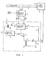
- Figure 1 is a block diagram which shows a load device in a data processing system which receives power from a power supply incorporating load anticipation control for proper regulation thereof.
- Figure 2 is a diagram of circuit for producing the load anticipation control of this invention for controlling the operation of a switching power supply.
- Figure 3 is a diagram of the circuitry of the
timer controller 22 of figure 2. - Referring now to figure 1 a load device is a powered by the output voltage VO on
line 17 from aswitching power supply 7. For the purposes of this illustration the load device is assumed to be a printer, although it will be understood that power supplies delivering power to other load devices can be similarly regulated in accordance. with this invention. The printer denoted asload 1 is a component of a data processing system which receives binary codes representative of alphanumeric characters to be printed along aprinter bus 2. These binary codes representative of alphanumeric codes to be printed are conveyed along theprinter bus 2 from well known printer control logic (not shown) which is not included in this invention. Also connected to theprinter bus 2, is aload anticipation controller 3 for assistance in the regulation ofpower supply 7, as is explained in more detail hereinafter. -
Load 1 may be representative of any load which reacts to particular data or other stimuli applied thereto to present a substantially predictable power requirement. The printer was chosen as an example of the type of device contemplated forload 1 because a data processing system printer presents a variety of predetermined loads in executing various ones of the possible commands that may be applied thereto. The execution of a carrier return command may present a first load. The printing of a comma character "," may present a second load. The printing of an "M" may present a third load, etc.. In practice, the printer may present various loadings on several input DC voltages applied thereto. For the purposes of simplicity in this description, only one DC voltage is shown as being applied to the printer, although those skilled in the art will understand the application of this invention to power supplies having multiple outputs to supply loads having multiple voltage requirements. - The
representative power supply 7 shown in figure 1 generally includes a combination of prior art regulation techniques such as those taugh by the Johari patent US-A-4,301,497, referenced above. An AC voltage is applied to a rectifier andfilter 9 to produce an unregulated DC voltage, V bulk, which is applied to the collector of aswitching transistor 12. The emitter of theswitching transistor 12 is connected to the primary of apower transformer 13. The other end of the primary of thepower transformer 13 is connected to ground. - The secondary circuit of the
power transformer 13 is connected in a flyback configuration including therectification diode 14 andfilter capacitor 15. - The conventional controller circuit 8 receives a feedback voltage, Vfb, along
line 16 from the output of the power supply. The controller 8 also includes a feed forward signal Vff, through thediode rectifier 19 from the output oftransformer 18 which is inputted with the AC voltage. Thus, the controller 8 is presented with signals representative of changes in the unregulated AC input signal in the form Vff, and in the regulated output signal in the form Vfb. From these input signals the base ofswitching transistor 12 is driven on and off, as appropriate, in an attempt to maintain a substantially constant output voltage VO. - The conventional controller 8 may take any of a variety of forms known in the prior art. Thus, the controller 8 may comprise a pulse width modulator operating at a constant frequency to vary the ratio of the on and off times of
transistor 12, although other controllers could also be employed. Some of the other types of controllers available operate with (a) constant on-time/variable frequency, (b) constant off- time/variable frequency, and (c) variable time and variable frequency. -
Line 5 from theload anticipation controller 3 to the conventional controller 8 is operable to override the "normal" command of the controller 8 to cause theswitching transistor 12 to be held in an off state, regardless of the conventional decision of controller 8. Likewise,line 6 from theload anticipation controller 3 to the controller 8 is operable to causeswitching transistor 12 to be held in an on state regardless of the conventional decision of the controller 8. Thus, the function of theload anticipation controller 3 is to monitor the current electrical load being presented byload 1, compare this load to the load requirement for execution of a predetermined command at a predetermined future time, and override the conventional controller 8 to force thepower supply 7, through the proper on-off control oftransistor 12, to make available to load 1, at the proper predetermined time, the amount of power required for execution of the code. - Referring now to figure 2 data byte from the
printer bus 2 are sampled by the load anticipation controller. The data bytes on theprinter bus 2 contain information concerning the future state of the loads. This is, these data bytes include information relative to what loads are to change, whether this change will be an increase or a decrease in loading, and when the load will change. More specifically, in an eight bit byte appearing onprinter bus 2, the lowest order three bits, for example, are referred to as the device selection bits and indicate the type of change in the loading which is to take place. In this example, if the lowest three bits in the byte are 110 this indicates that the character selection motor is the load which is to change, while a 010 indicates that the hammer is the load to change. Continuing this example, the fourth lowest order bit in the eight bit byte on theprinter bus 2 is referred to as the sequence bit and the state of this bit indicates whether the load described by the device selection bits is to be added to the existing load or dropped from the existing load. In this example, a "0" sequence bit denotes a pending load increase (i.e., the load described by the device selection bits will be turned on in the future), while a "1" sequence bit denotes a pending load decrease. - Additionally in this example, another bit (not necessarily a part of the eight bit byte) on the
printer bus 2 is referred to as the synchronize bit, and the state of this bit is pulsed from a low state to a high state for a short duration by the printer control logic at the time that the load described by the device selection bits is to change. The load controlled by the printer control logic will be either increased or decreased coincident with the rising edge of the pulsed synchronize bit. - In figure 2 the sequence is conveyed from the
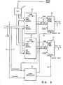
printer bus 2 alongline 20 to thetimer controller circuit 22 which is described in detail relative to figure 3.Line 21 conveys the status of the synchronize bit from theprinter bus 2 to thetimer controller 22. - The four lowest order bits including the three device selection bits and the sequence bit comprise the low order read only memory (hereinafter, ROM) addresses for the tables stored in
ROM 24 andROM 25. The high order addresses for the tables stored inROM converter 23 and conveyed along the highorder address bus 26 toROM 24 andROM 25. The A/D converter 23 is appropriately connected to the output ofpower supply 7, figure I, to sense the amount of power output frompower supply 7 presently being supplied to theload 1. The value of that amount of power is digitized by the A/D converter 23 and the digital representation of that amount of power represents the high order address in both of the read onlymemories - The values stored at the table addresses in
ROM 24 andROM 25 are digital representations of time increments. With a particular combination of device selection bits and sequence bit on theprinter bus 2 and a particular present power output frompower supply 7, a particular storage location in each of the read onlymemories ROM 24 is conveyed along the ontime bus 28 to preset a count downtimer 30. Similarly, the time increment stored at the address location ofROM 25 is conveyed along theoff time bus 29 to preset a count downtimer 31. Thereafter, in accordance with the ENABLE ON signal online 32 and the TRIGGER OFF signal online 33 from thetimer controller 32, and in synchronization with the CLOCK signals (which CLOCK signals may also, for example, be conveyed along bus 2) applied to the count downtimers timers lines transistor 12 in thepower supply 7. - The count down
timers timer controller 22. - Referring now to figure 3 the circuitry of the
timer controller 22 and its connections to the count downtimers gate 44 andINVERT 41 enables one of the ANDgates gate timers memories buses - The pulse from the synchronize bit also presets both storage positions of the 2 bit shift register 54 with binary 11111 values. The output of shift register 54 is conveyed along
line 55 to one input of each of ANDgates - Assuming, for this example, that the sequence bit applied to INVERT 41 is a zero, or low level, AND
gate 42 provides a high output at the time of the pulse from the synchronize bit and this high level is gated throughOR gate 45 and through the previously enabled ANDgate 46 to trigger online 33count dow timer 31 to start counting down to zero in synchronism with the CLOCK pulses applied thereto. During this count down time the HOLD OFF output online 5 of the count downtimer 31 is at a high level. Had the sequence bit been a one, a high level output from ANDgate 44 would have been gated throughOR gate 47 and ANDgate 48 to cause online 32 the count downtimer 30 to have been the first of the two count down timers to begin counting down. - When the output of the first of the two count down timers to count down goes to an up level, the up level is gated through
OR gate 52 to the SHIFT input of shift register 54. This causes a present "0" to be shifted into the lowest order bit position of shift register 54, and the "1" bit which previously occupied the lowest order bit position is shifted to the highest order bit position in the 2 bit shift register 54. - When count down
timer 31 reaches zero the negative going transition of the output signal thereof returning to a low level causes single shot 50 to provide an output pulse which is gated throughOR gate 47 to begin the count down oftimer 30. During the time thattimer 30 is counting down the HOLD ON output thereof online 6 is at a high level. Had count downtimer 30 been the first of the two count down timers to be operated, the negative going transition of its output, at the time that the level on the HOLD ON output returned to a low level, would have caused single shot 49 to provide a pulse which would have been gated throughOR gate 45 to start the count down oftimer 31. - When the output of the second of the two count down timers to count down goes to an up level, the up level is gated through
OR gate 52 to the shift input of shift register 54. This causes another present "0" to be shifted into the lowest order bit position of shift register 54, and the "0" bit which previously occupied the lowest order bit position is shifted to the highest order bit position in the 2 bit shift register 54. At this time, the output of shift register 54 online 55 goes low and the outputs of the count down timers can no longer trigger each other through the paths of the single shots. - Thus, a power supply system has been shown including load anticipation control for use in an environment wherein a power supply is subjected to varying loads which are anticipated before being placed across the power supply output. The "on" and "off" times of the power transformer primary switches are adjusted for optimum power supply response to the varying load.
- While the invention has been particularly shown and described wich reference to a preferred embodiment thereof, it will be understood by those skilled in the art that various other changes by equivalent means may be made such as, for example, selecting other types of memories or timers without departing from the scope of the invention as defined by the claims.
Claims (11)
Applications Claiming Priority (2)
| Application Number | Priority Date | Filing Date | Title |
|---|---|---|---|
| US06/377,531 US4425612A (en) | 1982-05-12 | 1982-05-12 | Power supply with load-transient anticipation |
| US377531 | 1982-05-12 |
Publications (2)
| Publication Number | Publication Date |
|---|---|
| EP0093902A1 true EP0093902A1 (en) | 1983-11-16 |
| EP0093902B1 EP0093902B1 (en) | 1985-12-11 |
Family
ID=23489483
Family Applications (1)
| Application Number | Title | Priority Date | Filing Date |
|---|---|---|---|
| EP83103806A Expired EP0093902B1 (en) | 1982-05-12 | 1983-04-20 | Power supply with load-transient anticipation |
Country Status (4)
| Country | Link |
|---|---|
| US (1) | US4425612A (en) |
| EP (1) | EP0093902B1 (en) |
| JP (1) | JPS58200318A (en) |
| DE (1) | DE3361473D1 (en) |
Cited By (8)
| Publication number | Priority date | Publication date | Assignee | Title |
|---|---|---|---|---|
| GB2157102A (en) * | 1984-03-01 | 1985-10-16 | Ronaldo Aguilar | Method and apparatus for amplitude control of varying parameters |
| EP1546834A2 (en) * | 2002-09-26 | 2005-06-29 | Itt Manufacturing Enterprises, Inc. | Power management system for variable load application |
| WO2007003967A2 (en) * | 2005-07-06 | 2007-01-11 | Cambridge Semiconductor Limited | Switch mode power supply control systems |
| EP1770848A2 (en) * | 2005-09-30 | 2007-04-04 | Hitachi Global Storage Technologies Netherlands B.V. | Voltage regulating systems responsive to feed-forward information from deterministic loads |
| WO2008060850A3 (en) * | 2006-10-31 | 2008-07-17 | Andrew Roman Gizara | Pulse width modulation sequence maintaining maximally flat voltage during current transients |
| USRE41596E1 (en) | 2003-07-31 | 2010-08-31 | Andrew Roman Gizara | System and method for integrating a digital core with a switch mode power supply |
| US7889019B2 (en) | 2006-10-13 | 2011-02-15 | Andrew Roman Gizara | Pulse width modulation sequence generating a near critical damped step response |
| CN101411048B (en) * | 2005-07-06 | 2012-03-07 | 剑桥半导体有限公司 | Switch mode power supply control systems |
Families Citing this family (20)
| Publication number | Priority date | Publication date | Assignee | Title |
|---|---|---|---|---|
| US4674031A (en) * | 1985-10-25 | 1987-06-16 | Cara Corporation | Peripheral power sequencer based on peripheral susceptibility to AC transients |
| US4823070A (en) * | 1986-11-18 | 1989-04-18 | Linear Technology Corporation | Switching voltage regulator circuit |
| FR2642237B1 (en) * | 1989-01-20 | 1996-06-21 | Thomson Csf | CONTROL DEVICE FOR CUT-OUT POWER SUPPLY AND CUT-OUT POWER SUPPLY PROVIDED WITH SUCH A DEVICE |
| US5079498A (en) * | 1991-03-26 | 1992-01-07 | Vickers Systems Limited | Digital pulse-width-modulation generator for current control |
| US5258903A (en) * | 1991-12-16 | 1993-11-02 | Thomson Consumer Electronics | Control circuit and power supply for televisions |
| JPH062607U (en) * | 1992-06-03 | 1994-01-14 | コーア株式会社 | Chip type semi-fixed resistor |
| US5406468A (en) * | 1993-09-02 | 1995-04-11 | Motorola, Inc. | Method for minimizing output transient responses in a power supply |
| US5422562A (en) * | 1994-01-19 | 1995-06-06 | Unitrode Corporation | Switching regulator with improved Dynamic response |
| US5916313A (en) * | 1996-10-31 | 1999-06-29 | Dell U. S. A., L.P. | Low cost power converter for a computer |
| US5859768A (en) | 1997-06-04 | 1999-01-12 | Motorola, Inc. | Power conversion integrated circuit and method for programming |
| US6718474B1 (en) | 2000-09-21 | 2004-04-06 | Stratus Technologies Bermuda Ltd. | Methods and apparatus for clock management based on environmental conditions |
| US6779862B2 (en) | 2002-09-12 | 2004-08-24 | Hewlett-Packard Development, L.P. | System and method of providing power to a print head |
| US6801027B2 (en) * | 2002-09-26 | 2004-10-05 | Itt Manufacturing Enterprises, Inc. | Power conversion in variable load applications |
| US6788038B1 (en) * | 2003-01-29 | 2004-09-07 | National Semiconductor Corporation | Apparatus and method for deactivating an on-switch of a circuit for a variable time interval |
| EP1653597A1 (en) * | 2004-10-28 | 2006-05-03 | Inventio Ag | Circuit arrangement for switched power supply |
| US7019503B1 (en) * | 2005-02-07 | 2006-03-28 | Raytheon Company | Active power filter with input voltage feedforward, output load feedforward, and output voltage feedforward |
| JP5190759B2 (en) * | 2008-01-08 | 2013-04-24 | 富士電機株式会社 | Power system |
| US7906950B2 (en) * | 2008-11-13 | 2011-03-15 | International Business Machines Corporation | Tuning a switching power supply |
| JP5526536B2 (en) * | 2008-12-18 | 2014-06-18 | 富士通株式会社 | Information processing apparatus, information processing system, program, and control apparatus |
| WO2020183024A1 (en) * | 2019-03-13 | 2020-09-17 | Advantest Corporation | Power supply, automated test equipment, method for operating a power supply, method for operating an automated test equipment and computer program using a voltage variation compensation mechanism |
Citations (3)
| Publication number | Priority date | Publication date | Assignee | Title |
|---|---|---|---|---|
| US4084103A (en) * | 1977-06-07 | 1978-04-11 | Burns Iii William Wesley | System-state and operating condition sensitive control method and apparatus for electric power delivery systems |
| GB2030736A (en) * | 1978-10-03 | 1980-04-10 | Palyn Associates Inc | Computer controlled power supply |
| EP0042043A1 (en) * | 1980-06-16 | 1981-12-23 | International Business Machines Corporation | Flyback converter with feedback and feed forward |
Family Cites Families (1)
| Publication number | Priority date | Publication date | Assignee | Title |
|---|---|---|---|---|
| JPS5213649A (en) * | 1975-07-23 | 1977-02-02 | Canon Inc | Device to control the power |
-
1982
- 1982-05-12 US US06/377,531 patent/US4425612A/en not_active Expired - Lifetime
-
1983
- 1983-04-12 JP JP58063118A patent/JPS58200318A/en active Granted
- 1983-04-20 EP EP83103806A patent/EP0093902B1/en not_active Expired
- 1983-04-20 DE DE8383103806T patent/DE3361473D1/en not_active Expired
Patent Citations (3)
| Publication number | Priority date | Publication date | Assignee | Title |
|---|---|---|---|---|
| US4084103A (en) * | 1977-06-07 | 1978-04-11 | Burns Iii William Wesley | System-state and operating condition sensitive control method and apparatus for electric power delivery systems |
| GB2030736A (en) * | 1978-10-03 | 1980-04-10 | Palyn Associates Inc | Computer controlled power supply |
| EP0042043A1 (en) * | 1980-06-16 | 1981-12-23 | International Business Machines Corporation | Flyback converter with feedback and feed forward |
Non-Patent Citations (2)
| Title |
|---|
| IBM TECHNICAL DISCLOSURE BULLETIN, vol. 23, no. 10, March 1981, New York C.L. ASHLEY et al. "Digital voltage regulator for switching power supplies", pages 4413-4414 * |
| Patent Abstracts of Japan vol. 3, no. 67, 9 June 1979 Page 55E116 & JP-A-54-45769 * |
Cited By (15)
| Publication number | Priority date | Publication date | Assignee | Title |
|---|---|---|---|---|
| GB2157102A (en) * | 1984-03-01 | 1985-10-16 | Ronaldo Aguilar | Method and apparatus for amplitude control of varying parameters |
| EP1546834A2 (en) * | 2002-09-26 | 2005-06-29 | Itt Manufacturing Enterprises, Inc. | Power management system for variable load application |
| EP1546834A4 (en) * | 2002-09-26 | 2007-08-08 | Itt Mfg Enterprises Inc | Power management system for variable load application |
| USRE41596E1 (en) | 2003-07-31 | 2010-08-31 | Andrew Roman Gizara | System and method for integrating a digital core with a switch mode power supply |
| US7504815B2 (en) | 2005-07-06 | 2009-03-17 | Cambridge Semiconductor Limited | Switch mode power supply control systems |
| WO2007003967A2 (en) * | 2005-07-06 | 2007-01-11 | Cambridge Semiconductor Limited | Switch mode power supply control systems |
| CN101411048B (en) * | 2005-07-06 | 2012-03-07 | 剑桥半导体有限公司 | Switch mode power supply control systems |
| WO2007003967A3 (en) * | 2005-07-06 | 2007-11-15 | Cambridge Semiconductor Ltd | Switch mode power supply control systems |
| EP1770848A3 (en) * | 2005-09-30 | 2008-04-30 | Hitachi Global Storage Technologies Netherlands B.V. | Voltage regulating systems responsive to feed-forward information from deterministic loads |
| US7957847B2 (en) | 2005-09-30 | 2011-06-07 | Hitachi Global Storage Technologies Netherlands, B.V. | Voltage regulating systems responsive to feed-forward information from deterministic loads |
| EP1770848A2 (en) * | 2005-09-30 | 2007-04-04 | Hitachi Global Storage Technologies Netherlands B.V. | Voltage regulating systems responsive to feed-forward information from deterministic loads |
| US7889019B2 (en) | 2006-10-13 | 2011-02-15 | Andrew Roman Gizara | Pulse width modulation sequence generating a near critical damped step response |
| US7719336B2 (en) | 2006-10-31 | 2010-05-18 | Andrew Roman Gizara | Pulse width modulation sequence maintaining maximally flat voltage during current transients |
| WO2008060850A3 (en) * | 2006-10-31 | 2008-07-17 | Andrew Roman Gizara | Pulse width modulation sequence maintaining maximally flat voltage during current transients |
| US7961023B2 (en) | 2006-10-31 | 2011-06-14 | Ipower Holdings Llc | Pulse width modulation sequence maintaining maximally flat voltage during current transients |
Also Published As
| Publication number | Publication date |
|---|---|
| JPH0217805B2 (en) | 1990-04-23 |
| JPS58200318A (en) | 1983-11-21 |
| US4425612A (en) | 1984-01-10 |
| EP0093902B1 (en) | 1985-12-11 |
| DE3361473D1 (en) | 1986-01-23 |
Similar Documents
| Publication | Publication Date | Title |
|---|---|---|
| EP0093902B1 (en) | Power supply with load-transient anticipation | |
| EP0877468B1 (en) | Programmable step down DC-DC converter controller | |
| EP0893876B1 (en) | Dynamic regulator for a dc-to-dc power converter and related methods | |
| US4714867A (en) | Method and apparatus for controlling a stepper motor with a programmable parabolic velocity profile | |
| US4504898A (en) | Start-up transient control for a DC-to-DC converter powered by a current-limited source | |
| EP0818875B1 (en) | Step-down type DC-DC regulator | |
| US4392103A (en) | Current sensing regulator | |
| US4066941A (en) | Motor drive control arrangements | |
| US3356928A (en) | Regulated rectifier for welding power supplies | |
| WO2001033310A1 (en) | Methods and apparatus to predictably change the output voltage of regulators | |
| US3577176A (en) | Constant current step motor system | |
| US6172885B1 (en) | Switched-mode power supply with mains current consumption regulation | |
| US10948934B1 (en) | Voltage regulator with piecewise linear loadlines | |
| US5594286A (en) | Power control system for electrical power supply modules | |
| US4569009A (en) | Switching regulator having a selectable gain amplifier for providing a selectively alterable output voltage | |
| EP1026689B1 (en) | Voltage down converter with switched hysteresis | |
| US5563498A (en) | Power supply regulator | |
| US8193801B2 (en) | Method and a device for feeding DC power to an amplifier module for a pulsed load | |
| CN113407022A (en) | CPU power supply system, control method and controller | |
| US5254937A (en) | Power supply control device having memory tables for providing a stabilized output | |
| RU2155425C1 (en) | Capacitor bank charging device | |
| EP0662747A2 (en) | A DC/DC converter for outputting multiple signals | |
| US4646218A (en) | Self-adjusting switched mode power supply | |
| US4598354A (en) | Data input and output device for a drive regulation apparatus operated by a digital computer | |
| EP0269214A2 (en) | Power supply and control systems for totem pole switches |
Legal Events
| Date | Code | Title | Description |
|---|---|---|---|
| PUAI | Public reference made under article 153(3) epc to a published international application that has entered the european phase |
Free format text: ORIGINAL CODE: 0009012 |
|
| AK | Designated contracting states |
Designated state(s): DE FR GB IT |
|
| 17P | Request for examination filed |
Effective date: 19840320 |
|
| GRAA | (expected) grant |
Free format text: ORIGINAL CODE: 0009210 |
|
| AK | Designated contracting states |
Designated state(s): DE FR GB IT |
|
| REF | Corresponds to: |
Ref document number: 3361473 Country of ref document: DE Date of ref document: 19860123 |
|
| ITF | It: translation for a ep patent filed | ||
| ET | Fr: translation filed | ||
| PLBE | No opposition filed within time limit |
Free format text: ORIGINAL CODE: 0009261 |
|
| STAA | Information on the status of an ep patent application or granted ep patent |
Free format text: STATUS: NO OPPOSITION FILED WITHIN TIME LIMIT |
|
| 26N | No opposition filed | ||
| ITTA | It: last paid annual fee | ||
| PGFP | Annual fee paid to national office [announced via postgrant information from national office to epo] |
Ref country code: GB Payment date: 19930324 Year of fee payment: 11 |
|
| PGFP | Annual fee paid to national office [announced via postgrant information from national office to epo] |
Ref country code: DE Payment date: 19930428 Year of fee payment: 11 |
|
| PGFP | Annual fee paid to national office [announced via postgrant information from national office to epo] |
Ref country code: FR Payment date: 19940330 Year of fee payment: 12 |
|
| PG25 | Lapsed in a contracting state [announced via postgrant information from national office to epo] |
Ref country code: GB Effective date: 19940420 |
|
| GBPC | Gb: european patent ceased through non-payment of renewal fee |
Effective date: 19940420 |
|
| PG25 | Lapsed in a contracting state [announced via postgrant information from national office to epo] |
Ref country code: DE Effective date: 19950103 |
|
| PG25 | Lapsed in a contracting state [announced via postgrant information from national office to epo] |
Ref country code: FR Effective date: 19951229 |
|
| REG | Reference to a national code |
Ref country code: FR Ref legal event code: ST |