EP0092985A2 - Dynamic memory device - Google Patents
Dynamic memory device Download PDFInfo
- Publication number
- EP0092985A2 EP0092985A2 EP83302285A EP83302285A EP0092985A2 EP 0092985 A2 EP0092985 A2 EP 0092985A2 EP 83302285 A EP83302285 A EP 83302285A EP 83302285 A EP83302285 A EP 83302285A EP 0092985 A2 EP0092985 A2 EP 0092985A2
- Authority
- EP
- European Patent Office
- Prior art keywords
- memory device
- dynamic memory
- charge
- coupled
- potential
- Prior art date
- Legal status (The legal status is an assumption and is not a legal conclusion. Google has not performed a legal analysis and makes no representation as to the accuracy of the status listed.)
- Granted
Links
Images


Classifications
-
- G—PHYSICS
- G11—INFORMATION STORAGE
- G11C—STATIC STORES
- G11C11/00—Digital stores characterised by the use of particular electric or magnetic storage elements; Storage elements therefor
- G11C11/21—Digital stores characterised by the use of particular electric or magnetic storage elements; Storage elements therefor using electric elements
- G11C11/34—Digital stores characterised by the use of particular electric or magnetic storage elements; Storage elements therefor using electric elements using semiconductor devices
- G11C11/40—Digital stores characterised by the use of particular electric or magnetic storage elements; Storage elements therefor using electric elements using semiconductor devices using transistors
- G11C11/401—Digital stores characterised by the use of particular electric or magnetic storage elements; Storage elements therefor using electric elements using semiconductor devices using transistors forming cells needing refreshing or charge regeneration, i.e. dynamic cells
- G11C11/403—Digital stores characterised by the use of particular electric or magnetic storage elements; Storage elements therefor using electric elements using semiconductor devices using transistors forming cells needing refreshing or charge regeneration, i.e. dynamic cells with charge regeneration common to a multiplicity of memory cells, i.e. external refresh
- G11C11/404—Digital stores characterised by the use of particular electric or magnetic storage elements; Storage elements therefor using electric elements using semiconductor devices using transistors forming cells needing refreshing or charge regeneration, i.e. dynamic cells with charge regeneration common to a multiplicity of memory cells, i.e. external refresh with one charge-transfer gate, e.g. MOS transistor, per cell
-
- H—ELECTRICITY
- H10—SEMICONDUCTOR DEVICES; ELECTRIC SOLID-STATE DEVICES NOT OTHERWISE PROVIDED FOR
- H10B—ELECTRONIC MEMORY DEVICES
- H10B12/00—Dynamic random access memory [DRAM] devices
- H10B12/30—DRAM devices comprising one-transistor - one-capacitor [1T-1C] memory cells
Definitions
- This invention relates to semiconductor memory devices and in particular to a dynamic memory device which substantially prevents soft errors caused by alpha particle radiation.
- each memory circuit comprises two elements including a single switching transistor and a charge storage capacitor.
- static memories incorporate six elements including two switching transistors having opposite states. Consequently, the additional charage created by the radiation may be drained off by the on transistor.
- static memory can also be adversely effected by radiation due to its higher density of components.
- the prior art has attempted to mitigate soft error problems by various techniques.
- One technique increases the storage density of the charge storage memory capacitor by either making the gate oxide thinner or changing the composition of gate oxide to increase its dielectric constant. Making the grate oxide thinner, however, increases the electric field thereby producing breakdown and associated reliability problems.
- changing the composition of the gate oxide is likewise ineffective since other compositions are not as reliable as Si0 2 and, at best, can only produce a small change in storage density. In any event, the purity of other compositions are still unknown and require further investigation and development.
- Another prior art technique utilizes a sensor amplifier coupled to the memory device and having improved sensitivity. By increasing the signal-to-noise ratio of the amplifier it can detect signal changes produced by the radiation. Such an amplifier, however, is impractical to construct since the S/N ratio is limited as the integration level increases. Furthermore, at larger integration levels the noise level increases.
- a further prior art technique utilizes chip coating.
- the memory chip is coated with a contamination-free organic material such as a polyimide resin.
- This technique does not prevent radiation which is generated by the chip composition itself and impurities within the chip package.
- the process of chip coating is costly and time consuming. While the industry has attempted to improve the purity of the chip itself and its packaging these attempts have been impractical.
- dynamic type memory devices have been designed by arranging unit memory cells in the form of a matrix as shown in Figure 1. That is, a switching MOS transistor Q 1 and a capacitor C are connected in series between a bit line BL and a power supply P O ; the gate electrode of transistor Q 1 is connected to a word line WL.
- the particular switching transistor of the unit memory cell which is selected by the word and bit line turns ON, so that a charge is stored in the capacitor which performs the memory operation. The stored charge is subsequently read out on the bit line via the switching transistor.
- Figure 2 shows a plane view of the pattern layout of the circuit of Figure 1, wherein one unit cell is surrounded by a dot-dashed line 11.
- WL 1 and WL 2 are word lines formed by a low resistance wiring layer.
- BL 1 and BL 2 are bit lines formed by, for example, an aluminum wiring layer, and
- C G is a low resistance layer for forming an opposite electrode of the capacitor.
- Switching MOS transistor. and MOS capacitor are represented by broken lines 12 and 13, respectively.
- the memory node N comprises a n-type diffused region wherein an opposite electrode P is connected to a power supply potential and the MOS capacitor is formed between the opposite electrode P and the node N.
- the dynamic memory device described above stores information by storing a charge in the capacitor, an erroneous reading can occur if the stored charge is lost by undesired leakage. Particularly, as discussed above, such erroneous readings are termed soft errors and are caused by alpha-radiation.
- the quantity of the charge stored in the capacitor is decreased as the circuit is constructed at higher integration densities. Therefore, the memory content is easily destroyed when alpha-particles impinge the semiconductor substrate.
- the alpha-rays applied to the semiconductor substrate 14 through its package generate a large number of electron-hole pairs along the trajectory of the radiation.
- femto-coulomb 10- 15 C.
- the carriers generated by alpha-rays are collected during an extremely short time period.
- the current waveform of the generated electrons flowing into region 15 is represented by a pulse current having a narrow pulse width as shown in Figure 4.
- the continuous time t d i.e., 0.2 to 0.3 n sec
- the electrical conductivity increases near the trajectory and the carriers are collected at the n-type region 15 along the trajectory. This is called funnelling effect. Since the electron-hole pairs are freely diffused into the semiconductor substrate 14, the high conductivity zone disappears after the time t d (hereinafter referred to as the funnelling time constant). Therefore, it is difficult to collect the carriers.
- the memory node N is a n-type region, and if a "1" is stored, the electrons flow easily into the n-type region because the potential is low. Consequently, a malfunction occurs whereby a stored "1" becomes a "O".
- the memory node capacitance is in the order of 40 fF, and the quantity of charge to be store is 200 fC (40 fF x 5 V) assuming the power supply voltage is 5 V. Since the total quantity of charge generated by the incident radiation is in the order of 100 fC, in the generated charge reaches 1/2 of the memory node capacitance. Accordingly, the likelihood that the memory content will be destroyed by carriers due to alpha-radiation is increased.
- this invention seeks to provide a dynamic memory device adapted to provide improved immunity to soft-errors due to alpha-particles, and the like, which permits high component density, and is superior in reliability and design flexibility.
- the improved device structure of the invention may also provide a simple method for eliminating soft errors without the time consuming and costly procedures employed in the prior art, without requiring a special gate oxide composition or thickness and avoiding the problems associated therewith, and despite the presence of radiation generating impurities in the chip itself and its packaging. ,
- an integrated semiconductor dynamic memory device adapted to provide improved immunity to particle radiation and comprising:
- a transistor Q l is a switch for transferring data between a bit line BL and a memory cell.
- the transistor gate potential is controlled by a control signal from a word line WL.
- the memory cell consists of a resistance element R and capacitive elements C 1 and C 2 .
- One end of the resistance element R and one end of the capacitive element C 1 are connected to a memory node N 31 , and the capacitive element C 2 is connected to the other end of the resistance element.
- the other ends of capacitive elements C 1 and C 2 are connected, respectively, to a reference potential, for example, ground potential.
- the memory cell is storing the memory condition "1" (i.e., the nodes N 31 and N 32 are maintained at a high potential). If alpha-particles irradiate N 31 , carriers will be generated resulting in the discharge of the charges stored by the capacitive element C 1 for a very short time period (i.e., within 0.2 to 0.3 ns as seen from Figure 4) due to the current Id. Since in a memory device having a high integration level, the charges stored in capacitive element C 1 are equal to or lower than the charges due to the current Id, all charges of capacitive element C 1 will be discharged in the worst case.
- the memory condition "1" i.e., the nodes N 31 and N 32 are maintained at a high potential.
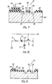
- isolation regions 16 and 18 having a thickness of 0.7 to 1 ⁇ m and composed of Si0 2 are provided on a p-type semiconductor substrate 20, for example, a Si substrate.
- N-type diffused regions 22, 24 and 26 are formed by introducing arsenic or phosphorus into the p-type semiconductor substrate.
- a gate electrode 28 composed of a polycrystalline silicon or metal silicide layer is provided on a gate insulating film 30 of Si0 2 having a thickness of about 350 ⁇ .
- one electrode 32 of the capacitive element, an electrode 34 contacting region 24 and a region 36 serving as the resistance element can all be produced at the same time and to a thickness of about 3000 A.
- an impurity is added to regions 32 and 34, but not to region 36 of the resistance element, for the purpose of lower the resistance value.
- MOS transistor Q 1 is provided by source and drain regions 24 and 26, and gate electrode 28.
- Capacitive element C 2 is provided by both electrode 32 and an inversion layer just under the electrode 32.
- Capacitive element C 1 is constituted by a stray capacitance of the source region 24. Preferably, this stray capacitance should be sufficiently low.
- the resistance element R may be locally provided in region 36, it is possible to distribute it within electrodes 32 and 34, and region 36.
- an impurity having an opposite conductivity to that of the semiconductor substrate may be introduced into the semiconductor substrate just under electrode 32 so as to increase the capacitance of capacitive element C 2 .
- Figure 7 shows isolation regions 38 and 40, composed of SI0 2 , having a thickness of 0.7 to 1 ⁇ m and provided on p-type semiconductor substrate 42.
- N-type diffused regions 44 and 46 are produced by introducing arsenic or phosphorus into the semiconductor substrate.
- a distributed resistance element region 48 composed of a polycrystalline silicon layer having a thickness, for example, of approximately 3000 R, is formed on the isolation region 38.
- Capacitor C 2 consists of region 48, a wiring layer 50 and an insulating film 52.
- Wiring layer 50 is deposited to a thickness of about 3000 X on insulating film 52 consisting of, for example, Si0 2 , Si 3 N 4 , or Ta0 2 and having a thickness of approximately 500 K.
- MOS transistor Q 1 consists of a gate electrode 54 formed on a gate insulating film 56, having a thickness of approximately 350 A, with source and drain regions 44 and 46.
- the structure of Figure 7 operates in a similar manner. Furthermore, the dynamic memory cell of Figure 7 is suitable for high packing density because the resistance element R and the capacitive element C 2 can be produced in the form of a multilayered structure.
- the earth potential is connected to region 22 as a reference potential.
- various electric potentials can be applied to wiring layer 50, such as a threshold voltage from a MOS transistor, a power supply voltage (e.g., 5 V), or an earth potential.
- a memory cell consists of a transistor Q 1 , capacitive elemnts C l and C 2 , and a resistance element R. One end of element R is connected to capacitive element C 2 .
- a signal charge is controlled by a word line WL, and the input and output of data are carried out through a bit line BL.
- Reference potentials for example, ground potential or power supply voltage are respectively connected to the capacitive element C 1 and the other end of the resistance element.
- This embodiment is different from the first embodiment in that resistance element R is connected to memory node N 31 through capacitive element C 2 . The operation of this memory cell is the same as that described with respect to the first embodiment.
- Figures 9 and 10 are structural modifications of the equivalent circuit shown in Figure 8.
- the portions of a transistor Q 1 are identical to those of the transistor shown in Figures 6 and 7.
- the capacitive element C 2 is provided by an Si0 2 insulating film 58 having a thickness of about 350 ⁇ , and an opposite facing electrode 60 consisting of a low resistivity polycrystalline silicon layer having a thickness of approximately 3000 A.
- a resistance element 62 is positioned adjacent one end of opposite electrode 60 and comprises, for example, a high resistivity polyerystalline silicon layer having a thickness of about 3000 ⁇ .
- a reference potential V R is supplied to an electrode 64 which has one end contiguous to the other end of resistance element 62.
- capacitive element C 2 consists of an Si0 2 insulating film 66 having a thickness of about 350 X, and an opposite facing electrode 68 consisting of a high resistivity polycrystalline silicon layer having a thickness of approximately 3000 X.
- An electrode 70 to which a reference voltage V R is applied is positioned so that one end is con- tinguous to one end of opposite electrode 68.
- the resistance element 68 is distributed over the insulating film 66.
- reference potential V R can be supplied from a power supply (e.g., 5 V), an earth potential, a substrate potential, or a threshold voltage from a MOS transistor.
- Figs. 11 and 12 show a structure wherein the electrode P opposite to memory node N in the circuit of Figure 1 consists of a high resistance wiring layer R and is connected to the word WL 1 of an adjacent line or power supply node P o , respectively.
- the time constant CR given by high resistance wiring layer R and memory node capacitance C is set so as to satisfy the relationship CR> t d (i.e., the funnelling time constant).
- Figures 13 and 14 show the pattern layouts of the third embodiment illustrated in Figure 11; Figure 13 is a plane view and Figure 14 is a cross-sectional view taken along the line A-A' of Figure 13.
- impurity ions are implanted into a capacitor portion 76 to provide an n + region.
- Capacitor portion 76 corresponds to memory node N of Figure 11.
- a high resistance polysilicon layer 78 is deposited thereon and is patterned to provide both a transfer gate 78' and a capacitor gate 78".
- capacitive element C consists of portions 72, 76 and 78".
- Portion 78" corresponds to electrode P of Figure 11 and also includes resistance layer R of Figure 11.
- impurity ions are selectively implanted into the substrate to form source and drain regions 80 and 82 of a switching MOS transistor.
- a contact junction 86 is made near the transfer gate, and a low resistance polysilicon layer 88 is deposited and patterned on film layer 84 and layer 78 of the transfer gate thereby forming parallel spaced word lines WL 1 and WL 2 .
- Contact junction 86 corresponds to CJ in Fig. 11.
- a layer insulation film 90 is formed on the second polysilicon layer 88 and the bit line BL 1 is formed by applying an aluminum interconnection layer 92.
- Bit line BL 1 has a contact junction with region 80.
- Figure 15 shows a pattern layout of Figure 12.
- WL 1 and WL 2 are adjacent word lines
- BL 1 and BL 2 are adjacent bit lines
- 94 is an opposite electrode of the cell (i.e., a high resistance layer)
- 96 is a low resistance wiring layer
- 98 is a contact junction between opposite electrode 94 and low resistance wiring layer 96.
- the resistor R of Figure 12 is distributed along the first high resistance layer. Portions 99 correspond to the memory node N of Figure 12
- electrode 94 corresponds to electrode P and resistance R of Figure 12
- layer 96 is coupled to a power supply and corresponds to the portion of Figure 12 between P o and R.
- Figure 16 shows a plane view of another pattern layout of the circuit of of Figure 12; however, this layout has the contact junction CJ between R and P of Figure 12.
- Separate memory cells are formed along a power supply line P o on either side.
- An opposite electrode 101 of capacitor C is formed which is separated from a high resistance layer 102 forming the other electrode of the capacitor for each of the cells, and power supply line P o is formed using a polysilicon layer to create a low resistance layer.
- Impurity ions for forming the high resistance portions are implanted into the polysilicon layer by using the broken line portions 100 as masks.
- the low resistance lines P o include a low resistance portion 103 which is connected to high resistance portion 102 and 100 via contact junction 98. According to this structure, since the broken line portions 100 and 102 have a high resistivity, an effect similar to the above-described embodiments can be obtained.
- the reference power supply lines P o are formed entirely by the low resistance wiring layers; if desired, the contact resistance of the junctions 98 between capacitor C and the power supply lines may be made high to achieve the same effect.
- layer 101 corresponds to memory node N of Figure 12, and portions 100 and 102 correspond to electrode P.
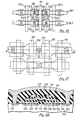
- Figures 17 and 18 shows the pattern layouts of a further modification of the circuit of Figure 12, wherein Figure 17 is a plane view and Figure 18 is a cross-sectional view taken along the line A-A' of Figure 12.
- Figure 17 has a contact junction between R and P of Figure 12.
- An isolation region 104 is formed on a semiconductor substrate 104, and impurity ions are implanted into a capacitor portion 106 to provide an n+ region.
- a high resistance polysilicon layer 108 is deposited on the substrate surface, and a layer insulation film 110 is provided after patterning the polysilicon layer. After a contact junction 112 is formed in the layer insulation film 110, a low resistance polysilicon layer 114 is deposited and patterned.
- first and second polysilicon layers 108 and 114 are shown to have the same pattern, this is not always necessary.
- a layer insulation film 116 is then formed on polysilicon layer 114, and a further low resistance polysilicon layer 118 is deposited on insulation film layer 116. Thereafter, impurity ions are selectively implanted into source and drain portions 120 and 122 of switching MOS transistor Q 1 .
- An insulation film layer 124 is formed on polysilicon layer 118, and a contact junction is formed with portions 120 by applying an aluminum wiring layer 126.
- Capacitor portion 106 corresponds to memory node N of Figure 12
- high resistance layer 108 corresponds to electrode P
- low resistance layer 114 corresponds to the lead portion including resistance R and power supply node P o .
- Contact junction 112 corresponds to junction CJ of Figure 12.
- FIG. 19 shows a cross-sectional view of another modification of the circuit illustrated in Figure 12, wherein the order of polysilicon layer 114 and polysilicon layer 118 are reversed. As shown, the same components as those of Figure 18 are represented by the same numberals and, therefore, further explanation is omitted. Similar operation and effect to the previously described embodiment is obtained by the structure of Figure 19.
- the memory cell If the memory cell is at a "1" state (i.e., the node N is at a high level) and alpha radiation is applied to node N, it collects electrons during an extremely short time period and node N changes its level to a low level. At that time, the potential of the opposite electrode P is reduced, due to capacitive coupling with node N, and then begins to recover slowly, during time constant CR, to level of the word line WV. The charge of the memory node is lost by this relaxation process. During an extremely short time period as compared with time constant CR, the opposite electrode may be regarded as in a floating condition, and the stored charge of capacitor C decreases as current flows through resistor R.
- node P begins to recover according to time constant CR
- the switch S is opened after the time t d and the transfer of charge does not occur.
- the final potential at the node N is lowered by V N [ 1 - exp(-t d /CR) ] wherein the intial potential is given by V N .
- the final potential is not sufficiently lowered if the relation of CR>t d is maintained. Accordingly, soft errors due to the incidence of alpha radiation can be substantially prevented.
- the malfunction caused by alpha radiation can be prevented because the resistance element and the capacitive element are connected in cascade with the data memory node and the charges stored in the capacitive element are not instantaneously discharged. Rather, the time constant of the discharge is determined by the resistance element and the capacitive element. Further, it is possible to accomplish high packing density for desirable high level integration since the capacitive and resistive elements can be provided in the form of a multilayered structure.
Landscapes
- Engineering & Computer Science (AREA)
- Microelectronics & Electronic Packaging (AREA)
- Computer Hardware Design (AREA)
- Semiconductor Memories (AREA)
Abstract
Description
- This invention relates to semiconductor memory devices and in particular to a dynamic memory device which substantially prevents soft errors caused by alpha particle radiation.
- As the semiconductor industry is continuing the trend toward higher levels of integration in memory circuits the presence of soft errors have become prevalent due to the passage of heavily-ionized radiation through the memory array area and resulting in the loss of stored data. When an alpha particle penetrates the surface of the memory substrate, it can create enough electron hole pairs near a storage node to cause a random, single bit error (i.e., soft error). These errors are caused by a substantial loss of stored charge in the memory storage capacitor of the semiconductor device. At smaller levels of integration (.e.g., 16K bit memories and smaller) the effect of alpha particle radiation on the stored charge is negligible since each capacitor maintains a relatively large capacitance and, thereby, a large charge. At higher levels of integration, however, the area of the storage capacitor is smaller which thereby reduces its capacitance; thus, the effect of radiation can appreciable effect the smaller stored charge and result in a change in the binary state of the memory.
- This problem is particularly acute in dynamic memories since each memory circuit comprises two elements including a single switching transistor and a charge storage capacitor. As a result, there is no means available to draw off the excess charge created by the radiation. Generally, static memories, on the other hand, incorporate six elements including two switching transistors having opposite states. Consequently, the additional charage created by the radiation may be drained off by the on transistor. At higher integration levels, however, static memory can also be adversely effected by radiation due to its higher density of components.
- The prior art has attempted to mitigate soft error problems by various techniques. One technique increases the storage density of the charge storage memory capacitor by either making the gate oxide thinner or changing the composition of gate oxide to increase its dielectric constant. Making the grate oxide thinner, however, increases the electric field thereby producing breakdown and associated reliability problems. Moreover, changing the composition of the gate oxide is likewise ineffective since other compositions are not as reliable as Si02 and, at best, can only produce a small change in storage density. In any event, the purity of other compositions are still unknown and require further investigation and development.
- Another prior art technique utilizes a sensor amplifier coupled to the memory device and having improved sensitivity. By increasing the signal-to-noise ratio of the amplifier it can detect signal changes produced by the radiation. Such an amplifier, however, is impractical to construct since the S/N ratio is limited as the integration level increases. Furthermore, at larger integration levels the noise level increases.
- A further prior art technique utilizes chip coating. With this method, the memory chip is coated with a contamination-free organic material such as a polyimide resin. This technique, however, does not prevent radiation which is generated by the chip composition itself and impurities within the chip package. Moreover, the process of chip coating is costly and time consuming. While the industry has attempted to improve the purity of the chip itself and its packaging these attempts have been impractical.
- The problems of the prior art memory devices discussed above will be explained with reference to Figures 1-3.
- Conventionally, dynamic type memory devices have been designed by arranging unit memory cells in the form of a matrix as shown in Figure 1. That is, a switching MOS transistor Q1 and a capacitor C are connected in series between a bit line BL and a power supply PO; the gate electrode of transistor Q1 is connected to a word line WL. The particular switching transistor of the unit memory cell which is selected by the word and bit line turns ON, so that a charge is stored in the capacitor which performs the memory operation. The stored charge is subsequently read out on the bit line via the switching transistor.
- Figure 2 shows a plane view of the pattern layout of the circuit of Figure 1, wherein one unit cell is surrounded by a dot-
dashed line 11. In the drawing WL1 and WL2 are word lines formed by a low resistance wiring layer. BL1 and BL2 are bit lines formed by, for example, an aluminum wiring layer, and CG is a low resistance layer for forming an opposite electrode of the capacitor. Switching MOS transistor. and MOS capacitor are represented bybroken lines - In an n-channel dynamic memory device formed on p-type semiconductor substrate, it is important to determine whether many elee- trons are present at a memory node N or whether a few electrons are present at node N; the first condition corresponds to a "0" (low level) and the second condition corresponds to a "1" (high level). The evaluation of the stored information ("1", "0") is accomplished by comparing the charge read out on the bit line with a reference charge of a dummy cell by utilizing a sensor amplifier. Usually, the memory node N comprises a n-type diffused region wherein an opposite electrode P is connected to a power supply potential and the MOS capacitor is formed between the opposite electrode P and the node N.
- Since the dynamic memory device described above stores information by storing a charge in the capacitor, an erroneous reading can occur if the stored charge is lost by undesired leakage. Particularly, as discussed above, such erroneous readings are termed soft errors and are caused by alpha-radiation. In the circuit configuration shown in Figures 1 and 2, the quantity of the charge stored in the capacitor is decreased as the circuit is constructed at higher integration densities. Therefore, the memory content is easily destroyed when alpha-particles impinge the semiconductor substrate. As shown in Figure 3, the alpha-rays applied to the
semiconductor substrate 14 through its package generate a large number of electron-hole pairs along the trajectory of the radiation. As a result, the total quantity of the change caused by the radiation is in the order of 100 fC (femto-coulomb = 10-15 C). Within the generated carriers, electrons with high mobility are likely to be collected if an n-type region 15 formed insubstrate 14 is positioned along the trajectory of the radiation. - On the one hand, it is known that the carriers generated by alpha-rays are collected during an extremely short time period. When alpha-rays wi- impinge an n-
type region 15, formed in a p-type substrate 14, the current waveform of the generated electrons flowing intoregion 15 is represented by a pulse current having a narrow pulse width as shown in Figure 4. The continuous time td (i.e., 0.2 to 0.3 n sec) of the pulse current is sufficiently short as compared with the internal node time constant of the LSI. During this time, since a large number of electron-hole pairs are produced along the trajectory of the radiation, the electrical conductivity increases near the trajectory and the carriers are collected at the n-type region 15 along the trajectory. This is called funnelling effect. Since the electron-hole pairs are freely diffused into thesemiconductor substrate 14, the high conductivity zone disappears after the time td (hereinafter referred to as the funnelling time constant). Therefore, it is difficult to collect the carriers. - With respect to the memory cell, the memory node N is a n-type region, and if a "1" is stored, the electrons flow easily into the n-type region because the potential is low. Consequently, a malfunction occurs whereby a stored "1" becomes a "O". In conventional devices, the memory node capacitance is in the order of 40 fF, and the quantity of charge to be store is 200 fC (40 fF x 5 V) assuming the power supply voltage is 5 V. Since the total quantity of charge generated by the incident radiation is in the order of 100 fC, in the generated charge reaches 1/2 of the memory node capacitance. Accordingly, the likelihood that the memory content will be destroyed by carriers due to alpha-radiation is increased. In order to reduce the soft error rate, it has become necessary, for example, to increase the memory node capacitance to a sufficiently large value to neglect the influence of carriers caused by alpha-rays. However, as discussed above, increasing the capacitance produces serious problems if high integration density is desired.
- Accordingly this invention seeks to provide a dynamic memory device adapted to provide improved immunity to soft-errors due to alpha-particles, and the like, which permits high component density, and is superior in reliability and design flexibility.
- The improved device structure of the invention may also provide a simple method for eliminating soft errors without the time consuming and costly procedures employed in the prior art, without requiring a special gate oxide composition or thickness and avoiding the problems associated therewith, and despite the presence of radiation generating impurities in the chip itself and its packaging. ,
- Accordingly the present invention provides an integrated semiconductor dynamic memory device adapted to provide improved immunity to particle radiation and comprising:
- a switching transistor (Ql) having a switching terminal, an input-output terminal and a memory terminal, a bit line (BL) coupled to said input-output terminal for supplying a charge to said transistor, a word line (WL) coupled to said switching terminal for controlling the switching of said transistor and charge storage means coupled to said memory terminal, characterised in that said charge storage means comprises R-C circuit means including a resistor (R) and a charge storage capacitor, for storing the charge supplied from said bit line in such a way as to substantially prevent loss of the stored charge due to particle radiation; and a potential reference coupled to said R-C circuit means.
- Some embodiments of the invention will now be described by way of example with reference to the accompanying drawings, in which:
- Figure 1 is an equivalent circuit of a conventional dynamic memory device;
- Figure 2 is a plan view of a pattern layout of the circuit shown in Figure 1;
- Figures 3 and 4 are a fragmentary sectional view and a graph respectively, for explaining the funnelling effect caused by particle radiation;
- Figure 5 is an equivalent circuit illustrating a first embodiment of the dynamic memory device in accordance with the invention;
- Figure 6 is a fragmentary sectional view illustrating the first embodiment of the present invention;
- Figure 7 is a fragmentary sectional view of a modification of the embodiment shown in Figure 6;
- Figure 8 is an equivalent circuit illustrating a second embodiment of the dynamic memory device in accordance with the invention;
- Figure 9 is a fragmentary sectional view illustrating the second embodiment of the present invention;
- Figure 10 is a fragmentary sectional view of a modification of the embodiment shown in Figure 9;
- Figure 11 is an equivalent circuit illustrating a third embodiment of the dynamic memory device in accordance with the invention;
- Figure 12 is an equivalent circuit illustrating a fourth embodiment of the present invention;
- Figure 13 is a fragmentary plan view of the third embodiment of the present invention;
- Figure 14 is a fragmentary sectional view of the third embodiment of the invention shown in Figure 13;
- Figures 15 to 17 are respective plan views illustrating separate modifications of the fourth embodiment of the present invention;
- Figure 18 is a fragmentary sectional view taken along line A-A' of Figure 17;
- Figure 19 is a fragmentary sectional view of a modification of the invention taken along line A-A' of Figure 17;
- Figure 20 is an equivalent circuit for explaining the operation of the third embodiment;
- Figure 21 is an equivalent circuit for explaining the operation of the fourth embodiment; and
- Figure 22 shows operating waveforms for explaining the operation of the present invention when alpha-radiation is applied.
- An equivalent circuit of a first embodiment of the dynamic memory device according to the present invention is shown in Figure 5. As shown, a transistor Ql is a switch for transferring data between a bit line BL and a memory cell. The transistor gate potential is controlled by a control signal from a word line WL. The memory cell consists of a resistance element R and capacitive elements C1 and C2. One end of the resistance element R and one end of the capacitive element C1 are connected to a memory node N31, and the capacitive element C2 is connected to the other end of the resistance element. The other ends of capacitive elements C1 and C2 are connected, respectively, to a reference potential, for example, ground potential.
- The operation of the dynamic memory device according to the present invention will now be described. Suppose that the memory cell is storing the memory condition "1" (i.e., the nodes N31 and N32 are maintained at a high potential). If alpha-particles irradiate N31, carriers will be generated resulting in the discharge of the charges stored by the capacitive element C1 for a very short time period (i.e., within 0.2 to 0.3 ns as seen from Figure 4) due to the current Id. Since in a memory device having a high integration level, the charges stored in capacitive element C1 are equal to or lower than the charges due to the current Id, all charges of capacitive element C1 will be discharged in the worst case. However, even if the capacitive element C1 is completely discharged, only a portion of the charges stored in capacitive element C2 will be discharged since its discharge rate depends upon the time constant of C2R. For example, if node N31 was completely discharged during td, the charges lost by node N32 are given by V0C2 [1- exp(-td/C2R)] . If the initial potential at node N32 is V0, the charges Q0, which are stored in capacitive elements C1 and C2 before the application of alpha-radiation become Q0 = V0 (C1 + C2). The total charges Qf remaining after the application of the radiation is given by:

- After the current Id caused by the radiation disappears, residual charges Qf are distributed to capacitive elements C1 and C2 through resistance element R. Accordingly, all of the stored charges are changed from QO to Qf. That is, all of the stored charges are reduced from 1 to C2 exp(-td/C2R)/(C1 + CZ). A sensing amplifier circuit will normally not detect a 10% or less change in the charge quantity. Therefore, if the values for resistance element R and capacitive elements C1 and C2 are selected so as to satisfy the expression
- C2 exp(-td/C2R)/(C1 + C2) ≥ 0.9, malfunction due to alpha radiation will not occur. For example, if during the time td wherein the pulse current Id is generated by alpha radiation and td = 0.3 ns, the capacitance values of elements Cl and C2 should be selected as C1 = 4 fF and C2 = 50 fF and the resistance value of element R should be selected as R = 210 K . In this case, however, it is necessary to position node N32 at a location electrically isolated from the substrate because a malfunction will not be prevented if alpha radiation is applied to node N32. Further, it is preferable to increase the value of resistance element R. In order to operate the memory cell at high speeds, however, it is necessary not to substantially increase this resistance as compared with the time constant determined by the conductance of transistor Q1 and capacitive elements Cl and C2.
- Two structural modifications of the first embodiment will now be described with reference to Figures 6 and 7. As shown in Figure 6,
isolation regions type semiconductor substrate 20, for example, a Si substrate. N-type diffusedregions gate electrode 28 composed of a polycrystalline silicon or metal silicide layer is provided on agate insulating film 30 of Si02 having a thickness of about 350 Å. When the electrodes are made of polycrystaline silicon, oneelectrode 32 of the capacitive element, anelectrode 34 contactingregion 24 and aregion 36 serving as the resistance element can all be produced at the same time and to a thickness of about 3000 A. In this case, an impurity is added toregions region 36 of the resistance element, for the purpose of lower the resistance value. - MOS transistor Q1 is provided by source and drain
regions gate electrode 28. Capacitive element C2 is provided by bothelectrode 32 and an inversion layer just under theelectrode 32. Capacitive element C1 is constituted by a stray capacitance of thesource region 24. Preferably, this stray capacitance should be sufficiently low. - Although the resistance element R may be locally provided in
region 36, it is possible to distribute it withinelectrodes region 36. In addition, an impurity having an opposite conductivity to that of the semiconductor substrate may be introduced into the semiconductor substrate just underelectrode 32 so as to increase the capacitance of capacitive element C2. - Figure 7 shows
isolation regions type semiconductor substrate 42. N-type diffusedregions resistance element region 48, composed of a polycrystalline silicon layer having a thickness, for example, of approximately 3000 R, is formed on theisolation region 38. Capacitor C2 consists ofregion 48, awiring layer 50 and an insulatingfilm 52.Wiring layer 50 is deposited to a thickness of about 3000 X on insulatingfilm 52 consisting of, for example, Si02, Si3N4, or Ta02 and having a thickness of approximately 500 K. MOS transistor Q1 consists of agate electrode 54 formed on agate insulating film 56, having a thickness of approximately 350 A, with source and drainregions - The operation of the structures shown in Figures 6 and 7 will now be explained. The transfer of data is carried out through the word line WL by using MOS transistor Q1. The input and output of data are accomplished by the bit line BL. In the structure of Figure 6, the entering signal charge is supplied to the capacitive element formed by
electrode 32 from the stray capacitance of thesource region 24 viaresistance element 36 and the inversion layer produced just under theelectrode 32. When alpha radiation is applied near thesource region 24, the charges stored in the stray capacitance are lost since the incident radiation generates charges mainly within the semiconductor substrate. However, the charges formed by the radiation does not effect the charges stored in the capacitance formed by the inversion layer. Accordinly, a malfunction will not occur in the memory cell. The structure of Figure 7 operates in a similar manner. Furthermore, the dynamic memory cell of Figure 7 is suitable for high packing density because the resistance element R and the capacitive element C2 can be produced in the form of a multilayered structure. In Figure 6, the earth potential is connected toregion 22 as a reference potential. In Figure 7, however, various electric potentials can be applied towiring layer 50, such as a threshold voltage from a MOS transistor, a power supply voltage (e.g., 5 V), or an earth potential. - A second embodiment of a dynamic memory device according to the present invention will be described with reference to Figs. 8-10. A memory cell consists of a transistor Q1, capacitive elemnts Cl and C2, and a resistance element R. One end of element R is connected to capacitive element C2. A signal charge is controlled by a word line WL, and the input and output of data are carried out through a bit line BL. Reference potentials, for example, ground potential or power supply voltage are respectively connected to the capacitive element C1 and the other end of the resistance element. This embodiment is different from the first embodiment in that resistance element R is connected to memory node N31 through capacitive element C2. The operation of this memory cell is the same as that described with respect to the first embodiment.
- Figures 9 and 10 are structural modifications of the equivalent circuit shown in Figure 8. In Figures 9 and 10, the portions of a transistor Q1 are identical to those of the transistor shown in Figures 6 and 7. In Figure 9, the capacitive element C2 is provided by an Si02 insulating film 58 having a thickness of about 350 Å, and an
opposite facing electrode 60 consisting of a low resistivity polycrystalline silicon layer having a thickness of approximately 3000 A. Aresistance element 62 is positioned adjacent one end ofopposite electrode 60 and comprises, for example, a high resistivity polyerystalline silicon layer having a thickness of about 3000 Å. Further, a reference potential VR is supplied to anelectrode 64 which has one end contiguous to the other end ofresistance element 62. In Figure 10, capacitive element C2 consists of an Si02 insulating film 66 having a thickness of about 350 X, and anopposite facing electrode 68 consisting of a high resistivity polycrystalline silicon layer having a thickness of approximately 3000 X. Anelectrode 70 to which a reference voltage VR is applied is positioned so that one end is con- tinguous to one end ofopposite electrode 68. As shown in Figure 10 theresistance element 68 is distributed over the insulatingfilm 66. As discussed regarding the first embodiment, reference potential VR can be supplied from a power supply (e.g., 5 V), an earth potential, a substrate potential, or a threshold voltage from a MOS transistor. - The third and fourth embodiments of the present invention will now be described with reference to Figures 11-15. Figs. 11 and 12 show a structure wherein the electrode P opposite to memory node N in the circuit of Figure 1 consists of a high resistance wiring layer R and is connected to the word WL1 of an adjacent line or power supply node Po, respectively. The time constant CR, given by high resistance wiring layer R and memory node capacitance C is set so as to satisfy the relationship CR> td (i.e., the funnelling time constant).
- Figures 13 and 14 show the pattern layouts of the third embodiment illustrated in Figure 11; Figure 13 is a plane view and Figure 14 is a cross-sectional view taken along the line A-A' of Figure 13. After forming an
isolation region 72 on asemiconductor substrate 74, impurity ions are implanted into acapacitor portion 76 to provide an n+ region.Capacitor portion 76 corresponds to memory node N of Figure 11. After a gate insulating film is formed on the substrate surface, a highresistance polysilicon layer 78 is deposited thereon and is patterned to provide both a transfer gate 78' and acapacitor gate 78". Thus, capacitive element C consists ofportions Portion 78" corresponds to electrode P of Figure 11 and also includes resistance layer R of Figure 11. Using thepolysilicon layer 78 as a mask, impurity ions are selectively implanted into the substrate to form source and drainregions insulation film layer 84, acontact junction 86 is made near the transfer gate, and a lowresistance polysilicon layer 88 is deposited and patterned onfilm layer 84 andlayer 78 of the transfer gate thereby forming parallel spaced word lines WL1 and WL2.Contact junction 86 corresponds to CJ in Fig. 11. Thereafter, alayer insulation film 90 is formed on thesecond polysilicon layer 88 and the bit line BL1 is formed by applying analuminum interconnection layer 92. Bit line BL1 has a contact junction withregion 80. - Figure 15 shows a pattern layout of Figure 12. As shown, WL1 and WL2 are adjacent word lines, BL1 and BL2 are adjacent bit lines, 94 is an opposite electrode of the cell (i.e., a high resistance layer), 96 is a low resistance wiring layer, and 98 is a contact junction between
opposite electrode 94 and lowresistance wiring layer 96. In this structure, the resistor R of Figure 12 is distributed along the first high resistance layer.Portions 99 correspond to the memory node N of Figure 12,electrode 94 corresponds to electrode P and resistance R of Figure 12, andlayer 96 is coupled to a power supply and corresponds to the portion of Figure 12 between Po and R. - The present invention will not be limited to the described embodiments, it is clearly possible to embody the invention by other modifications. For example, the present invention may be employed in the structure of Figure 16. Figure 16 shows a plane view of another pattern layout of the circuit of of Figure 12; however, this layout has the contact junction CJ between R and P of Figure 12. Separate memory cells are formed along a power supply line Po on either side. An
opposite electrode 101 of capacitor C is formed which is separated from ahigh resistance layer 102 forming the other electrode of the capacitor for each of the cells, and power supply line Po is formed using a polysilicon layer to create a low resistance layer. Impurity ions for forming the high resistance portions are implanted into the polysilicon layer by using thebroken line portions 100 as masks. The low resistance lines Po include alow resistance portion 103 which is connected tohigh resistance portion contact junction 98. According to this structure, since thebroken line portions junctions 98 between capacitor C and the power supply lines may be made high to achieve the same effect. Thus,layer 101 corresponds to memory node N of Figure 12, andportions - Figures 17 and 18 shows the pattern layouts of a further modification of the circuit of Figure 12, wherein Figure 17 is a plane view and Figure 18 is a cross-sectional view taken along the line A-A' of Figure 12. Like Figure 16, Figure 17 has a contact junction between R and P of Figure 12. An
isolation region 104 is formed on asemiconductor substrate 104, and impurity ions are implanted into acapacitor portion 106 to provide an n+ region. A highresistance polysilicon layer 108 is deposited on the substrate surface, and alayer insulation film 110 is provided after patterning the polysilicon layer. After acontact junction 112 is formed in thelayer insulation film 110, a lowresistance polysilicon layer 114 is deposited and patterned. Although the first and second polysilicon layers 108 and 114 are shown to have the same pattern, this is not always necessary. Alayer insulation film 116 is then formed onpolysilicon layer 114, and a further lowresistance polysilicon layer 118 is deposited oninsulation film layer 116. Thereafter, impurity ions are selectively implanted into source and drainportions insulation film layer 124 is formed onpolysilicon layer 118, and a contact junction is formed withportions 120 by applying analuminum wiring layer 126.Capacitor portion 106 corresponds to memory node N of Figure 12,high resistance layer 108 corresponds to electrode P, whilelow resistance layer 114 corresponds to the lead portion including resistance R and power supply node Po. Contact junction 112 corresponds to junction CJ of Figure 12. - The present invention is not limited to the above described embodiments, it is also possible to incorporate other various modifications. For example, the present invention may be constructed as shown in Figure 19. Figure 19 shows a cross-sectional view of another modification of the circuit illustrated in Figure 12, wherein the order of
polysilicon layer 114 andpolysilicon layer 118 are reversed. As shown, the same components as those of Figure 18 are represented by the same numberals and, therefore, further explanation is omitted. Similar operation and effect to the previously described embodiment is obtained by the structure of Figure 19. - The operation of the above-described structures will now be explained. If the memory cell is at a "1" state (i.e., the node N is at a high level) and alpha radiation is applied to node N, it collects electrons during an extremely short time period and node N changes its level to a low level. At that time, the potential of the opposite electrode P is reduced, due to capacitive coupling with node N, and then begins to recover slowly, during time constant CR, to level of the word line WV. The charge of the memory node is lost by this relaxation process. During an extremely short time period as compared with time constant CR, the opposite electrode may be regarded as in a floating condition, and the stored charge of capacitor C decreases as current flows through resistor R. On the one hand, after the short time period td (i.e., 0.2 to 0.3 n see) electrons caused by the radiation are no longer collected. Accordingly, since alpha radiation generated current does not flow into node N, further loss of charge does not occur. Consequently, the stored charge is lost only in accordance with the CR time constant during the time period td. Consequently, the loss of stored charges can be greatly reduced by properly selecting the value for resistor R.
- This operation is more clearly described by reference to the circuits of Figures 20 and 21. As shown, generation of carriers due to alpha radiation and the effect of their collection are represented by a capacitor C and a switch S. Capacitor C corresponds to the charge generated by alpha radiation and the switch S is closed only during the time period td and opened thereafter. The operating waveforms are shown in Figure 22: If alpha-rays are applied to node N, carriers are produced so that a charge in order of 100 fC is stored in capacitor C and switch S is closed. At this time, although both nodes N and P are immediately reduced to a low level, the charge stored in the cell is not yet lost. Although node P begins to recover according to time constant CR, the switch S is opened after the time td and the transfer of charge does not occur. In the process described above, the final potential at the node N is lowered by VN [ 1 - exp(-td/CR) ] wherein the intial potential is given by VN. Thus, the final potential is not sufficiently lowered if the relation of CR>td is maintained. Accordingly, soft errors due to the incidence of alpha radiation can be substantially prevented.
- According to this present invention, even if alpha-rays are applied to the memory device, the malfunction caused by alpha radiation can be prevented because the resistance element and the capacitive element are connected in cascade with the data memory node and the charges stored in the capacitive element are not instantaneously discharged. Rather, the time constant of the discharge is determined by the resistance element and the capacitive element. Further, it is possible to accomplish high packing density for desirable high level integration since the capacitive and resistive elements can be provided in the form of a multilayered structure.
Claims (10)
Applications Claiming Priority (8)
| Application Number | Priority Date | Filing Date | Title |
|---|---|---|---|
| JP57070403A JPS5948549B2 (en) | 1982-04-28 | 1982-04-28 | dynamic storage device |
| JP70403/82 | 1982-04-28 | ||
| JP57085742A JPS5948550B2 (en) | 1982-05-21 | 1982-05-21 | Dynamic storage device |
| JP57085744A JPS5948552B2 (en) | 1982-05-21 | 1982-05-21 | Dynamic storage device |
| JP57085743A JPS5948551B2 (en) | 1982-05-21 | 1982-05-21 | Dynamic storage device |
| JP85744/82 | 1982-05-21 | ||
| JP85743/82 | 1982-05-21 | ||
| JP86742/82 | 1982-05-21 |
Publications (3)
| Publication Number | Publication Date |
|---|---|
| EP0092985A2 true EP0092985A2 (en) | 1983-11-02 |
| EP0092985A3 EP0092985A3 (en) | 1985-09-18 |
| EP0092985B1 EP0092985B1 (en) | 1989-04-19 |
Family
ID=27465240
Family Applications (1)
| Application Number | Title | Priority Date | Filing Date |
|---|---|---|---|
| EP83302285A Expired EP0092985B1 (en) | 1982-04-28 | 1983-04-21 | Dynamic memory device |
Country Status (3)
| Country | Link |
|---|---|
| US (1) | US4641165A (en) |
| EP (1) | EP0092985B1 (en) |
| CA (1) | CA1199725A (en) |
Families Citing this family (16)
| Publication number | Priority date | Publication date | Assignee | Title |
|---|---|---|---|---|
| JPH0685431B2 (en) * | 1985-06-10 | 1994-10-26 | 株式会社日立製作所 | Semiconductor device |
| US4805138A (en) * | 1985-08-23 | 1989-02-14 | Texas Instruments Incorporated | An unerasable eprom cell |
| JPS62145859A (en) * | 1985-12-20 | 1987-06-29 | Mitsubishi Electric Corp | Semiconductor memory |
| JPH0713871B2 (en) * | 1987-06-11 | 1995-02-15 | 三菱電機株式会社 | Dynamic RAM |
| US5003361A (en) * | 1987-08-31 | 1991-03-26 | At&T Bell Laboratories | Active dynamic memory cell |
| US5075570A (en) * | 1987-11-25 | 1991-12-24 | Honeywell Inc. | Switching state retention circuit having a feedback loop stabilizing capacitance |
| CA1293570C (en) * | 1988-05-27 | 1991-12-24 | Ian Thomson | Radon detector |
| US5048023A (en) * | 1989-02-16 | 1991-09-10 | The United States Of America As Represented By The Administrator, National Aeronautics And Space Administration | Asymmetric soft-error resistant memory |
| JPH05136363A (en) * | 1991-11-15 | 1993-06-01 | Sharp Corp | Semiconductor memory device |
| JP3615285B2 (en) * | 1995-09-29 | 2005-02-02 | 日本バーブラウン株式会社 | Differential filter circuit and integrated circuit structure thereof |
| US6888187B2 (en) * | 2002-08-26 | 2005-05-03 | International Business Machines Corporation | DRAM cell with enhanced SER immunity |
| US7078306B1 (en) | 2003-03-24 | 2006-07-18 | Integrated Device Technology, Inc. | Method for forming a thin film resistor structure |
| US7921400B1 (en) | 2005-07-20 | 2011-04-05 | Integrated Device Technology, Inc. | Method for forming integrated circuit device using cell library with soft error resistant logic cells |
| US8999764B2 (en) * | 2007-08-10 | 2015-04-07 | International Business Machines Corporation | Ionizing radiation blocking in IC chip to reduce soft errors |
| US10396082B2 (en) | 2017-07-05 | 2019-08-27 | Micron Technology, Inc. | Memory cells having a controlled-conductivity region |
| JP7182930B2 (en) * | 2018-07-24 | 2022-12-05 | キヤノン株式会社 | radiation detector |
Citations (5)
| Publication number | Priority date | Publication date | Assignee | Title |
|---|---|---|---|---|
| US4115871A (en) * | 1977-04-19 | 1978-09-19 | National Semiconductor Corporation | MOS random memory array |
| EP0013173A2 (en) * | 1978-12-26 | 1980-07-09 | The Board Of Trustees Of The Leland Stanford Junior University | Monolithic distributed resistor-capacitor device utilizing polycrystalline semiconductor material |
| JPS561559A (en) * | 1979-06-19 | 1981-01-09 | Fujitsu Ltd | One-transistor type dynamic memory cell |
| EP0025325A2 (en) * | 1979-08-30 | 1981-03-18 | Fujitsu Limited | Semiconductor memory device and the process for producing the same |
| JPS56107390A (en) * | 1980-01-29 | 1981-08-26 | Nec Corp | Semiconductor memory device |
Family Cites Families (8)
| Publication number | Priority date | Publication date | Assignee | Title |
|---|---|---|---|---|
| US4060796A (en) * | 1975-04-11 | 1977-11-29 | Fujitsu Limited | Semiconductor memory device |
| US4164751A (en) * | 1976-11-10 | 1979-08-14 | Texas Instruments Incorporated | High capacity dynamic ram cell |
| US4112575A (en) * | 1976-12-20 | 1978-09-12 | Texas Instruments Incorporated | Fabrication methods for the high capacity ram cell |
| JPS5950102B2 (en) * | 1977-01-12 | 1984-12-06 | 日本電気株式会社 | semiconductor memory device |
| JPS544086A (en) * | 1977-06-10 | 1979-01-12 | Fujitsu Ltd | Memory circuit unit |
| US4240195A (en) * | 1978-09-15 | 1980-12-23 | Bell Telephone Laboratories, Incorporated | Dynamic random access memory |
| JPS5846070B2 (en) * | 1979-02-13 | 1983-10-14 | 松下電器産業株式会社 | solid-state imaging device |
| JPS5832789B2 (en) * | 1980-07-18 | 1983-07-15 | 富士通株式会社 | semiconductor memory |
-
1983
- 1983-03-15 US US06/475,554 patent/US4641165A/en not_active Expired - Lifetime
- 1983-04-21 EP EP83302285A patent/EP0092985B1/en not_active Expired
- 1983-04-27 CA CA000426852A patent/CA1199725A/en not_active Expired
Patent Citations (5)
| Publication number | Priority date | Publication date | Assignee | Title |
|---|---|---|---|---|
| US4115871A (en) * | 1977-04-19 | 1978-09-19 | National Semiconductor Corporation | MOS random memory array |
| EP0013173A2 (en) * | 1978-12-26 | 1980-07-09 | The Board Of Trustees Of The Leland Stanford Junior University | Monolithic distributed resistor-capacitor device utilizing polycrystalline semiconductor material |
| JPS561559A (en) * | 1979-06-19 | 1981-01-09 | Fujitsu Ltd | One-transistor type dynamic memory cell |
| EP0025325A2 (en) * | 1979-08-30 | 1981-03-18 | Fujitsu Limited | Semiconductor memory device and the process for producing the same |
| JPS56107390A (en) * | 1980-01-29 | 1981-08-26 | Nec Corp | Semiconductor memory device |
Non-Patent Citations (2)
| Title |
|---|
| PATENTS ABSTRACTS OF JAPAN, vol. 5, no. 177(P-89)(849), 13th November 1981; & JP-A-56 107 390 (NIPPON DENKI K.K.) 26-08-1981 * |
| PATENTS ABSTRACTS OF JAPAN, vol. 5, no. 51(E-51)(723), 10th April 1981; & JP-A-56 001 559 (FUJITSU K.K.) 09-01-1981 * |
Also Published As
| Publication number | Publication date |
|---|---|
| CA1199725A (en) | 1986-01-21 |
| EP0092985A3 (en) | 1985-09-18 |
| US4641165A (en) | 1987-02-03 |
| EP0092985B1 (en) | 1989-04-19 |
Similar Documents
| Publication | Publication Date | Title |
|---|---|---|
| US4641165A (en) | Dynamic memory device with an RC circuit for inhibiting the effects of alpha particle radiation | |
| US3819959A (en) | Two phase charge-coupled semiconductor device | |
| US6323536B1 (en) | Method and apparatus for forming a junctionless antifuse | |
| KR900003908B1 (en) | Dynamic random access memory cell having double floor structure | |
| US4146902A (en) | Irreversible semiconductor switching element and semiconductor memory device utilizing the same | |
| US4158239A (en) | Resistive gate FET flip-flop storage cell | |
| US4070653A (en) | Random access memory cell with ion implanted resistor element | |
| US7489164B2 (en) | Multi-port memory devices | |
| US6975041B2 (en) | Semiconductor storage device having high soft-error immunity | |
| US4849801A (en) | Semiconductor memory device having increased capacitance for the storing nodes of the memory cells | |
| US6271568B1 (en) | Voltage controlled resistance modulation for single event upset immunity | |
| US4282446A (en) | High density floating gate EPROM programmable by charge storage | |
| EP0238549B1 (en) | Nonvolatile memory cell | |
| JPH09508240A (en) | Ferroelectric memory | |
| US5053848A (en) | Apparatus for providing single event upset resistance for semiconductor devices | |
| US5310694A (en) | Method for forming a transistor device with resistive coupling | |
| US4695864A (en) | Dynamic storage device with extended information holding time | |
| KR830001767B1 (en) | Non-Destructive Stop Isostatic Memory | |
| GB1563479A (en) | Semiconductor memory cell circuits | |
| US4330849A (en) | Complementary semiconductor memory device | |
| US4432073A (en) | Semiconductor memory device | |
| US4797725A (en) | Memory cell for SRAM with a dielectric layer over a gate electrode to provide a parallel resistive and capacitive element | |
| JPS6062153A (en) | Resistive gate type field effect transistor logic circuit | |
| KR19980069994A (en) | Semiconductor device and manufacturing method thereof | |
| JPS6150372A (en) | Method of producing semiconductor device |
Legal Events
| Date | Code | Title | Description |
|---|---|---|---|
| PUAI | Public reference made under article 153(3) epc to a published international application that has entered the european phase |
Free format text: ORIGINAL CODE: 0009012 |
|
| AK | Designated contracting states |
Designated state(s): DE FR GB IT |
|
| RAP1 | Party data changed (applicant data changed or rights of an application transferred) |
Owner name: KABUSHIKI KAISHA TOSHIBA |
|
| PUAL | Search report despatched |
Free format text: ORIGINAL CODE: 0009013 |
|
| AK | Designated contracting states |
Designated state(s): DE FR GB IT |
|
| 17P | Request for examination filed |
Effective date: 19860221 |
|
| 17Q | First examination report despatched |
Effective date: 19870911 |
|
| GRAA | (expected) grant |
Free format text: ORIGINAL CODE: 0009210 |
|
| AK | Designated contracting states |
Kind code of ref document: B1 Designated state(s): DE FR GB IT |
|
| ITF | It: translation for a ep patent filed |
Owner name: STUDIO CONS. BREVETTUALE S.R.L. |
|
| REF | Corresponds to: |
Ref document number: 3379702 Country of ref document: DE Date of ref document: 19890524 |
|
| ET | Fr: translation filed | ||
| PLBE | No opposition filed within time limit |
Free format text: ORIGINAL CODE: 0009261 |
|
| STAA | Information on the status of an ep patent application or granted ep patent |
Free format text: STATUS: NO OPPOSITION FILED WITHIN TIME LIMIT |
|
| 26N | No opposition filed | ||
| ITTA | It: last paid annual fee | ||
| PGFP | Annual fee paid to national office [announced via postgrant information from national office to epo] |
Ref country code: FR Payment date: 19970409 Year of fee payment: 15 |
|
| PGFP | Annual fee paid to national office [announced via postgrant information from national office to epo] |
Ref country code: GB Payment date: 19970414 Year of fee payment: 15 |
|
| PGFP | Annual fee paid to national office [announced via postgrant information from national office to epo] |
Ref country code: DE Payment date: 19970428 Year of fee payment: 15 |
|
| PG25 | Lapsed in a contracting state [announced via postgrant information from national office to epo] |
Ref country code: GB Free format text: LAPSE BECAUSE OF NON-PAYMENT OF DUE FEES Effective date: 19980421 |
|
| PG25 | Lapsed in a contracting state [announced via postgrant information from national office to epo] |
Ref country code: FR Free format text: THE PATENT HAS BEEN ANNULLED BY A DECISION OF A NATIONAL AUTHORITY Effective date: 19980430 |
|
| GBPC | Gb: european patent ceased through non-payment of renewal fee |
Effective date: 19980421 |
|
| PG25 | Lapsed in a contracting state [announced via postgrant information from national office to epo] |
Ref country code: DE Free format text: LAPSE BECAUSE OF NON-PAYMENT OF DUE FEES Effective date: 19990202 |
|
| REG | Reference to a national code |
Ref country code: FR Ref legal event code: ST |