EP0092902A2 - D.C. controlled adjustable ramp signal generator and method - Google Patents
D.C. controlled adjustable ramp signal generator and method Download PDFInfo
- Publication number
- EP0092902A2 EP0092902A2 EP83301249A EP83301249A EP0092902A2 EP 0092902 A2 EP0092902 A2 EP 0092902A2 EP 83301249 A EP83301249 A EP 83301249A EP 83301249 A EP83301249 A EP 83301249A EP 0092902 A2 EP0092902 A2 EP 0092902A2
- Authority
- EP
- European Patent Office
- Prior art keywords
- coupled
- reference voltage
- output
- adjustable
- voltage
- Prior art date
- Legal status (The legal status is an assumption and is not a legal conclusion. Google has not performed a legal analysis and makes no representation as to the accuracy of the status listed.)
- Granted
Links
Images

Classifications
-
- H—ELECTRICITY
- H03—ELECTRONIC CIRCUITRY
- H03K—PULSE TECHNIQUE
- H03K4/00—Generating pulses having essentially a finite slope or stepped portions
- H03K4/94—Generating pulses having essentially a finite slope or stepped portions having trapezoidal shape
-
- G—PHYSICS
- G11—INFORMATION STORAGE
- G11B—INFORMATION STORAGE BASED ON RELATIVE MOVEMENT BETWEEN RECORD CARRIER AND TRANSDUCER
- G11B5/00—Recording by magnetisation or demagnetisation of a record carrier; Reproducing by magnetic means; Record carriers therefor
- G11B5/02—Recording, reproducing, or erasing methods; Read, write or erase circuits therefor
Definitions
- the present invention relates to a circuit and method for generating a ramp signal having a D.C. controlled adjustable level and it is particularly useful for generation and automatic control of bias recording or erase signals in magnetic recording devices.
- a desired high frequency audio bias recording or erase signal envelope level has to be switched on and off gradually, that is ramped-up or ramped-down, respectively, to avoid the recording of an undesirable audible "pop" on the magnetic medium.
- an optimum bias or erase level of an audio signal to be recorded has to be reached in a relatively short time for editing purposes, preferably within one video field or frame interval, that is within 30 milliseconds or less. Therefore, it is desirable to maintain a predetermined ramping period for respectively selected optimum signal levels within the operating range.
- a prior art video tape recorder type VPR-2, manufactured by Ampex Corporation, the present applicant, utilizes for recording audio signals a ramped bias and erase signal generator circuit described in VPR-2 Video Production Recorder, Catalog No. 1809384-02, Page 10-7, issued in May 1980.
- that prior art circuit (not shown) has an integrating operational amplifier for providing a desired ramped output voltage in reponse to an input voltage step.
- a voltage limiter connected to the integrator limits the output voltage therefrom to a value determined by a master bias level commonly applied as a D.C. reference voltage to all the recording channels.
- the limited ramped output signal from the integrator is then chopped by a solid state switch at a desired bias or erase signal frequency, and thereafter filtered to obtain a ramped high frequency sine wave signal.
- the thereby obtained signal is then attenuated by a potentiometer attenuator connected in the high frequency signal path in each respective channel to obtain respective desired optimum levels and thereafter the resulting attenuated signal is applied to a respective bias or erase current amplifier of that particular channel as it is well known in the art.
- the above-described prior art circuit has the following disadvantages. Every time when the master bias level is changed the duration of the ramp also changes. Consequently during edits on tape when the "ramp-down" or “ramp-up” portion of a previously recorded information overlaps with a ramp portion of a newly recorded information going in the opposite direction, "holes” or “thumps” may be formed in the recorded signal envelope which in turn cause sudden disturbing changes in the edited audio signal volume.
- Another disadvantage is that the prior art circuit is not suitable for automatic control since the attenuator is located in the high frequency signal path, that is, at a remote location from the D.C. control circuit.
- the prior art circuit configuration cannot be readily adapted for use with printed wire boards.
- potentiometers are exposed to signal level losses for example due to the temperature changes, or when utilized in multichannel recorders, to losses induced by interchannel crosstalk.
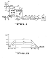
- FIG. 1 shows a block diagram of a preferred. embodiment of the invention which is described below.
- An adjustable D.C. voltage source and control circuit 10 provides at its output 9 a selected D.C. reference voltage value Vref which is applied via line 11 to a voltage limiter 12.
- Circuit 10 may be implemented for example by a suitable D.C. voltage source and an adjustable voltage divider such as a potentiometer 5 connected to a D.C. power supply to obtain a desired adjustable Vref value as is known in the art.
- the circuit 10 may also comprise a suitable digital control circuit such as comprising an analog-to-digital converter, a microcomputer with memory which may be programmed to provide desired optimum Vref values and a digital-to-analog converter for converting the digital value obtained from the computer into an analog voltage, as will be described later in more detail with reference to FIG. 3.
- a suitable digital control circuit such as comprising an analog-to-digital converter, a microcomputer with memory which may be programmed to provide desired optimum Vref values and a digital-to-analog converter for converting the digital value obtained from the computer into an analog voltage, as will be described later in more detail with reference to FIG. 3.
- the above-indicated D.C. reference voltage Vref on line 11 is also applied to one terminal 13 of a voltage divider 14 comprising series resistors 15, 16 having respective resistance values Rl, R2, while an opposite terminal 17 of the divider 14 is grounded.
- An output terminal 18 of the voltage divider 14 providing an output voltage Vdiv is connected via line 19 to a non-inverting input 20 of an integrating operational amplifier 21 whose inverting input 22 is connected via a series resistor 23 having a value R' and via line 24 to a switch 7.
- An input terminal 6 connected to the switch 7 receives a control signal in the form of a positive or negative D.C. voltage step.
- Switch 7 is driven via resistor 4 by the reference voltage Vref at output 9 from circuit 10.
- Switch 7 is preferably implemented by a suitable solid state switch such as a field-effect transistor.
- a feedback capacitor 26 having a value C is connected between an output 25 and the inverting input 22 of integrator 21. -In parallel with capacitor 26 there is connected the previously mentioned voltage limiter 12.
- the output 25 of integrator 21 is coupled via line 27 to an input of a chopper 28 whose output is coupled via line 29 to an input of a filter circuit 30.
- An output of the filter circuit 30 is in turn connected via line 31 to an input of a drive amplifier 32 whose output is coupled to an input of an erase or bias recording magnetic head circuit 34.
- Chopper 28 is utilized to provide a high frequency square wave signal whose envelope corresponds to the output signal from integrator 21 and its frequency corresponds to a desired erase or bias signal frequency to be recorded.
- Filter 30 is utilized to provide a high frequency sine wave signal from the above-indicated square wave signal and drive amplifier 32 is utilized as a power amplifier to amplify the high frequency sine wave signal and to apply the same to a magnetic recording or erase head 34, as is well known.
- the circuit 10 is adjusted by potentiometer 5 to provide a desired D.C. voltage level at its output 9 corresponding to an optimum bias or erase signal envelope level Vref as it is known in the art.
- voltage characteristics a, b, c, having respective optimum levels Va, Vb, Vc are shown in FIG. 2.
- a control signal in the form of a positive or negative voltage step (not shown) received at input terminal 6 effects a voltage step of opposite direction from switch 7 on line 24.
- the switch 7 serves to couple the inverting input 22 of the amplifier 25 via the input resistor 23 either to the datum (i.e. ground) for Vref, when the switch 7 is conductive or substantially to Vref, when the switch is non-conductive.
- a negative voltage step produced when the switch 7 is made conductive is applied via series resistor 23 to the inverting input 22 of integrator 21.
- a positive going linear voltage ramp is provided at output 25 of the integrator as shown during time period Tl of FIG. 2.
- the limiter 12 limits the excursion of the positive going ramp voltage to a selected value such as shown by any of the previously mentioned values Va to Vc and thereafter maintains that value constant until a negative goingramp is initiated by a positive step voltage produced at input 22 of integrator 21 by the switch 7.
- the non-inverting input 20 of integrator 21 receives via line 19 a voltage Vdiv which is equal to a predetermined ratio of the selected reference voltage Vref obtained at output 9 of control circuit 10. Consequently, when Vref is changed, the voltage Vdiv at non-inverting input 20 of integrator 21 changes in linear proportion therewith while maintaining a constant ratio between the reference voltage Vref on line 11 and the output voltage Vdiv from divider 14 on line 19.
- Equation (1) may be easily derived from the well known theory of integrating circuits.
- FIG. 3 showing a circuit diagram of another preferred embodiment of the invention which in part corresponds to the above-described circuit of FIG. 1. It is noted that corresponding circuit elements in all the respective drawing figures are designated by similar reference numerals to facilitate comparison.
- FIG. 3 shows a preferred embodiment of the invention which provides automatic control taking into consideration the above-indicated parameters.
- a desired reference voltage level common to all the channels such as the previously mentioned master signal level Vmst may be set by an operator utilizing a potentiometer 5 described before with reference to FIG.I.
- the signal Vmst is applied via line 50 to an analog-to-digital converter.51, for example type AD7574 manufactured by Analog Devices Corp.
- the corresponding digital signal from A/ D converter 51 is applied via an address and data bus 55 to a digital control circuit with memory 53, in a manner well known in the art.
- circuit 53 may be implemented by a microcomputer. Type 8048 manufactured by Intel Corporation.
- the microcomputer stores in its memory data pertaining to the above-indicated respective characteristic parameters of each channel.
- the stored data may indicate respective desired percentages of different master voltage levels Vmst necessary to obtain an optimuim reference voltage Vref for each channel.
- the microcomputer 53 is connected via bus 55 to respective latching digital-to-analog converters 56, 57, etc., each pertaining to one recording channel.
- circuits 56, 57 may be selected as type AM6080 manufactured by Advanced Micro Devices Corporation.
- the microcomputer 53 sequentialy addresses the respective latching D/A converters 56, 57, etc., and applies a digital signal thereto corresponding to an optimum value Vrefl, Vref2, etc., as required by each channel.
- each converter 56, 57, etc. digital values are converted into corresponding analog values by each converter 56, 57, etc., and applied to the analog portion of the circuit of FIG. 3 in a manner corresponding to that previously described with reference to FIG. 1.
- the latching D/A circuit 56 of channel 1 applies a reference voltage Vrefl on line 11 to the voltage divider 14 and limiter 12, respectively, as it is shown in FIG. 3 and as it has been described above.
- latches 60, 61, etc. for example type 74LS74 are utilized to apply the previously described positive or negative control voltage step Vconl, Vcon2, etc., to a respective switch of each channel, such as switch 7 of channel 1.
- the respective latches 60, 61, etc. are controlled via the address and data bus 55 from the microcomputer 53 in response to a control signal received thereby for example from a control panel 54.
- the control panel 54 may comprise control switches for selecting an individual recording channel and a desired operation mode as is well known in the art and as illustrated by switches designated CH1 to CHn within the control panel 54.
- switch CHl on control panel 54 when a particular channel, such as channel 1 is selected for recording, switch CHl on control panel 54 is set by the operator in a corresponding position, while control panel 54 applies a corresponding signal via bus 55 to microcomputer 53.
- the microcomputer 53 addresses latch 60 and applies a corresponding control signal thereto.
- Latch 60 in turn applies a positive control voltage step Vcon on line 6 to switch 7, thus initiating an increasing ramp signal on line 27, as it has been described previously.
- switch CH1 when it is desired to interrupt the recording mode in channel 1, switch CH1 is turned to a corresponding position thus effecting the latch 60 to be controlled via bus 55 to apply an opposite voltage step Vcon which in turn effects a decreasing ramp signal on line 27.
- the limiter 12 of FIG. 1 is implemented by a transistor having its emitter connected to the output 25 of integrator 21, while its collector is coupled to the inverting input 22 of the integrator.
- the base of transistor 12 is connected via line 11 to the output 9 of the adjustable D.C. voltage source and control circuit 10, wherefrom it obtains the previously described optimum reference voltage Vref. Consequently, when Vref is applied to the base 8 of transistor 21, the output voltage therefrom is limited to the maximum emitter-to-collector voltage as determined by Vref.
- a clamping diode 41 is coupled between the respective inputs 20, 22 of amplifier 21 to maintain a predetermined voltage difference therebetween.
- FIG. 4 shows an alternative embodiment of a portion of the above-described circuit of FIG. 3 as follows.
- the integrating operational amplifier is implemeted by a CMOS type amplifier 40.
- the reference voltage Vref on line 11 is applied directly into Vcc source voltage input of amplifier 40 which voltage sets the limit for a maximum output signal value on line 27 from the operational amplifier 40.
- the voltage limiter 12 of FIGS. 1 and 3 is omitted while the operation of the integrator 40 remains substantially the same as previously described with reference to FIG. 1 and 3.
- the remaining portions of the circuits of FIGS. 1, 3 and 4 are similar and are designated by like reference numerals to facilitate comparison and consequently their description will not be repeated herein with respect to FIG. 4.
Landscapes
- Analogue/Digital Conversion (AREA)
Abstract
Description
- The present invention relates to a circuit and method for generating a ramp signal having a D.C. controlled adjustable level and it is particularly useful for generation and automatic control of bias recording or erase signals in magnetic recording devices.
- As it is well known in the art of magnetic recording a desired high frequency audio bias recording or erase signal envelope level has to be switched on and off gradually, that is ramped-up or ramped-down, respectively, to avoid the recording of an undesirable audible "pop" on the magnetic medium. When utilized for example in video tape recorders, an optimum bias or erase level of an audio signal to be recorded has to be reached in a relatively short time for editing purposes, preferably within one video field or frame interval, that is within 30 milliseconds or less. Therefore, it is desirable to maintain a predetermined ramping period for respectively selected optimum signal levels within the operating range.
- As an example, a prior art video tape recorder, type VPR-2, manufactured by Ampex Corporation, the present applicant, utilizes for recording audio signals a ramped bias and erase signal generator circuit described in VPR-2 Video Production Recorder, Catalog No. 1809384-02, Page 10-7, issued in May 1980. Briefly, that prior art circuit (not shown) has an integrating operational amplifier for providing a desired ramped output voltage in reponse to an input voltage step. A voltage limiter connected to the integrator limits the output voltage therefrom to a value determined by a master bias level commonly applied as a D.C. reference voltage to all the recording channels. The limited ramped output signal from the integrator is then chopped by a solid state switch at a desired bias or erase signal frequency, and thereafter filtered to obtain a ramped high frequency sine wave signal. The thereby obtained signal is then attenuated by a potentiometer attenuator connected in the high frequency signal path in each respective channel to obtain respective desired optimum levels and thereafter the resulting attenuated signal is applied to a respective bias or erase current amplifier of that particular channel as it is well known in the art.
- The above-described prior art circuit has the following disadvantages. Every time when the master bias level is changed the duration of the ramp also changes. Consequently during edits on tape when the "ramp-down" or "ramp-up" portion of a previously recorded information overlaps with a ramp portion of a newly recorded information going in the opposite direction, "holes" or "thumps" may be formed in the recorded signal envelope which in turn cause sudden disturbing changes in the edited audio signal volume. Another disadvantage is that the prior art circuit is not suitable for automatic control since the attenuator is located in the high frequency signal path, that is, at a remote location from the D.C. control circuit. The prior art circuit configuration cannot be readily adapted for use with printed wire boards. Moreover, as it is well known such potentiometers are exposed to signal level losses for example due to the temperature changes, or when utilized in multichannel recorders, to losses induced by interchannel crosstalk.
- Consequently, it is an object of the invention to provide a circuit and method for generating a ramp signal which has a D.C. controlled adjustable level.
- It is a preferred object to provide a circuit and method for generating a ramp signal having a predetermined ramping period which is maintained constant within a range of operating optimum signal levels.
- It is another preferred object or advantage to provide an , automatically controlled erase or bias ramp signal generator circuit and method suitable for use in single channel or multi- channel magnetic recorders.
- It is a further preferred object or advantage to provide a circuit and method having the above-indicated features while being suitable for economical production.
-
- FIG. 1 is a circuit diagram of a preferred embodiment of the invention.
- FIG. 2 shows respective ramp signal characteristics having different optimum D.C. levels as provided by the preferred embodiment .
- FIG. 3 is a circuit diagram of another preferred embodiment of the invention.
- . FIG. 4. is an alternative embodiment of a portion of the circuit of FIGS. 1 or 3.
- FIG. 1 shows a block diagram of a preferred. embodiment of the invention which is described below. An adjustable D.C. voltage source and
control circuit 10 provides at its output 9 a selected D.C. reference voltage value Vref which is applied via line 11 to avoltage limiter 12.Circuit 10 may be implemented for example by a suitable D.C. voltage source and an adjustable voltage divider such as apotentiometer 5 connected to a D.C. power supply to obtain a desired adjustable Vref value as is known in the art. Alternatively, thecircuit 10 may also comprise a suitable digital control circuit such as comprising an analog-to-digital converter, a microcomputer with memory which may be programmed to provide desired optimum Vref values and a digital-to-analog converter for converting the digital value obtained from the computer into an analog voltage, as will be described later in more detail with reference to FIG. 3. The above-indicated D.C. reference voltage Vref on line 11 is also applied to oneterminal 13 of a voltage divider 14 comprisingseries resistors opposite terminal 17 of the divider 14 is grounded. Anoutput terminal 18 of the voltage divider 14 providing an output voltage Vdiv is connected vialine 19 to anon-inverting input 20 of an integrating operational amplifier 21 whoseinverting input 22 is connected via aseries resistor 23 having a value R' and vialine 24 to aswitch 7. Aninput terminal 6 connected to theswitch 7 receives a control signal in the form of a positive or negative D.C. voltage step.Switch 7 is driven via resistor 4 by the reference voltage Vref atoutput 9 fromcircuit 10. Switch 7 is preferably implemented by a suitable solid state switch such as a field-effect transistor. - A
feedback capacitor 26 having a value C is connected between anoutput 25 and the invertinginput 22 of integrator 21. -In parallel withcapacitor 26 there is connected the previously mentionedvoltage limiter 12. - The
output 25 of integrator 21 is coupled vialine 27 to an input of achopper 28 whose output is coupled vialine 29 to an input of afilter circuit 30. An output of thefilter circuit 30 is in turn connected vialine 31 to an input of adrive amplifier 32 whose output is coupled to an input of an erase or bias recordingmagnetic head circuit 34. - The
respective circuits output 25 of integrator 21 of FIG. 1 are well known in the art, for example, from the above-indicated Catalog and therefore they will be described only briefly herein.Chopper 28 is utilized to provide a high frequency square wave signal whose envelope corresponds to the output signal from integrator 21 and its frequency corresponds to a desired erase or bias signal frequency to be recorded.Filter 30 is utilized to provide a high frequency sine wave signal from the above-indicated square wave signal anddrive amplifier 32 is utilized as a power amplifier to amplify the high frequency sine wave signal and to apply the same to a magnetic recording orerase head 34, as is well known. - Now the operation of the circuit of FIG. 1 will be described with reference to the characteristics of FIG. 2.
- The
circuit 10 is adjusted bypotentiometer 5 to provide a desired D.C. voltage level at itsoutput 9 corresponding to an optimum bias or erase signal envelope level Vref as it is known in the art. As an example, voltage characteristics a, b, c, having respective optimum levels Va, Vb, Vc are shown in FIG. 2. A control signal in the form of a positive or negative voltage step (not shown) received atinput terminal 6 effects a voltage step of opposite direction fromswitch 7 online 24. Theswitch 7 serves to couple the invertinginput 22 of theamplifier 25 via theinput resistor 23 either to the datum (i.e. ground) for Vref, when theswitch 7 is conductive or substantially to Vref, when the switch is non-conductive. - A negative voltage step produced when the
switch 7 is made conductive is applied viaseries resistor 23 to the invertinginput 22 of integrator 21. Thus a positive going linear voltage ramp is provided atoutput 25 of the integrator as shown during time period Tl of FIG. 2. Thelimiter 12 limits the excursion of the positive going ramp voltage to a selected value such as shown by any of the previously mentioned values Va to Vc and thereafter maintains that value constant until a negative goingramp is initiated by a positive step voltage produced atinput 22 of integrator 21 by theswitch 7. - There is an important difference and advantage in the operation of the circuit of FIG. 1 over the prior art circuits as follows. The
non-inverting input 20 of integrator 21 receives via line 19 a voltage Vdiv which is equal to a predetermined ratio of the selected reference voltage Vref obtained atoutput 9 ofcontrol circuit 10. Consequently, when Vref is changed, the voltage Vdiv atnon-inverting input 20 of integrator 21 changes in linear proportion therewith while maintaining a constant ratio between the reference voltage Vref on line 11 and the output voltage Vdiv from divider 14 online 19. In the preferred embodiment the respective resistor values of the voltage divider 14 are selected equal, that is Rl = R2. Accordingly, the above-indicated voltage ratio is Vref: Vdiv = 2:1. As a result, the "ramp-up" and "ramp-down" periods shown in FIG. 2 are equal, that is
series resistor 23 and C is a selected capacitance value ofcapacitor 26. Equation (1) may be easily derived from the well known theory of integrating circuits. - It will be understood by those skilled in the art that while the above-indicated ratio 1:1 of the resistor values Rl, R2 is particularly useful in audio bias signal recording or erase of the preferred embodiment, in other applications it may become desirable to select different resistance ratios such as 1:2, 2:3, etc., to obtain different time periods Tl, T2 and thus to provide different ramp-up and ramp-down slopes of the voltage envelope, respectively.
- It is seen from the foregoing description that while the voltage Vdiv at
input 20 of the integrator 21 is derived from the reference voltage Vref on line 11 as a selected portion thereof, the same voltage Vref also determines the voltage limit provided by the integrator 21 at itsoutput 25. Thus the voltage Vdiv atinput 20 changes in a known linear proportion with a change of the selected voltage limit on line 11. However, whenever the voltage Vref from the control circuit is changed to provide a new optimum voltage level on line 11, as is shown for example in FIG., 2 by the characteristics a to c, the above-described time intervals of the preferred embodiment remain the same, that is Tl = T2 as previously indicated by equation (1) while the slope of the ramp changes within that interval to obtain the changed optimum voltage level Va to Vc. - It is also seen that a desired ramp as well as a desired optimum level of the high frequency signal envelope are respectively obtained by utilizing D.C. voltage control means, while use of a conventional potentiometer attenuator in the high frequency signal path is eliminated in the circuit of the invention. Consequently, the circuit in accordance with the invention does not suffer from signal level losses due to temperature changes or, when utilized in multi-channel recorder, from interchannel crosstalk induced in potentiometers which are utilized for high frequency signal attenuation in the prior art circuits.
- Now FIG. 3 will be described, showing a circuit diagram of another preferred embodiment of the invention which in part corresponds to the above-described circuit of FIG. 1. It is noted that corresponding circuit elements in all the respective drawing figures are designated by similar reference numerals to facilitate comparison.
- As it follows from the foregoing description, it is a significant advantage of the present invention that it may be utilized as an automatically controlled ramp signal generating circuit, such as for generation of bias or erase signals. An example of s.uch a circuit is shown in FIG. 3 and will be described below. In certain applications, for example in high quality multichannel audio recorders it is of great importance to obtain flexibility in generation of desired optimum bias and erase signal levels for each channel, to maintain stability of these levels, as well as accurate ramping and timing of these signals such as for editing purposes. As it is well known, in multichannel devices each channel may require a slightly different optimum signal level due to the differences in the characteristics of these channels. FIG. 3 shows a preferred embodiment of the invention which provides automatic control taking into consideration the above-indicated parameters. For example, a desired reference voltage level common to all the channels, such as the previously mentioned master signal level Vmst may be set by an operator utilizing a
potentiometer 5 described before with reference to FIG.I. The signal Vmst is applied vialine 50 to an analog-to-digital converter.51, for example type AD7574 manufactured by Analog Devices Corp. The corresponding digital signal from A/Dconverter 51 is applied via an address anddata bus 55 to a digital control circuit withmemory 53, in a manner well known in the art. For example,circuit 53 may be implemented by a microcomputer. Type 8048 manufactured by Intel Corporation. The microcomputer stores in its memory data pertaining to the above-indicated respective characteristic parameters of each channel. For example, the stored data may indicate respective desired percentages of different master voltage levels Vmst necessary to obtain an optimuim reference voltage Vref for each channel. Themicrocomputer 53 is connected viabus 55 to respective latching digital-to-analog converters example circuits microcomputer 53 sequentialy addresses the respective latching D/A converters converter A circuit 56 of channel 1 applies a reference voltage Vrefl on line 11 to the voltage divider 14 andlimiter 12, respectively, as it is shown in FIG. 3 and as it has been described above. - In the circuit of FIG. 3 latches 60, 61, etc., for example type 74LS74 are utilized to apply the previously described positive or negative control voltage step Vconl, Vcon2, etc., to a respective switch of each channel, such as
switch 7 of channel 1. The respective latches 60, 61, etc., are controlled via the address anddata bus 55 from themicrocomputer 53 in response to a control signal received thereby for example from acontrol panel 54. Thecontrol panel 54 may comprise control switches for selecting an individual recording channel and a desired operation mode as is well known in the art and as illustrated by switches designated CH1 to CHn within thecontrol panel 54. - Thus, when a particular channel, such as channel 1 is selected for recording, switch CHl on
control panel 54 is set by the operator in a corresponding position, whilecontrol panel 54 applies a corresponding signal viabus 55 tomicrocomputer 53. Themicrocomputer 53 in turn addresses latch 60 and applies a corresponding control signal thereto.Latch 60 in turn applies a positive control voltage step Vcon online 6 to switch 7, thus initiating an increasing ramp signal online 27, as it has been described previously. Analogously, when it is desired to interrupt the recording mode in channel 1, switch CH1 is turned to a corresponding position thus effecting thelatch 60 to be controlled viabus 55 to apply an opposite voltage step Vcon which in turn effects a decreasing ramp signal online 27. - It will be understood from the foregoing description that while only one recording channel is shown in detail in FIG. 3, any desired number of similar channels may be controlled by the
control circuit 10 of FIG. 3 in a manner described above. - In the embodiment of FIG. 3 the
limiter 12 of FIG. 1 is implemented by a transistor having its emitter connected to theoutput 25 of integrator 21, while its collector is coupled to the invertinginput 22 of the integrator. The base oftransistor 12 is connected via line 11 to theoutput 9 of the adjustable D.C. voltage source andcontrol circuit 10, wherefrom it obtains the previously described optimum reference voltage Vref. Consequently, when Vref is applied to thebase 8 of transistor 21, the output voltage therefrom is limited to the maximum emitter-to-collector voltage as determined by Vref. A clampingdiode 41 is coupled between therespective inputs - FIG. 4 shows an alternative embodiment of a portion of the above-described circuit of FIG. 3 as follows. Instead of a bipolar transistor type amplifier shown at 21 in FIG. 1 the integrating operational amplifier is implemeted by a
CMOS type amplifier 40. In the embodiment of FIG. 4 the reference voltage Vref on line 11 is applied directly into Vcc source voltage input ofamplifier 40 which voltage sets the limit for a maximum output signal value online 27 from theoperational amplifier 40. It is seen that in the embodiment of FIG. 4 thevoltage limiter 12 of FIGS. 1 and 3 is omitted while the operation of theintegrator 40 remains substantially the same as previously described with reference to FIG. 1 and 3. It is noted that the remaining portions of the circuits of FIGS. 1, 3 and 4 are similar and are designated by like reference numerals to facilitate comparison and consequently their description will not be repeated herein with respect to FIG. 4. - While the invention has been shown and described with particular reference to preferred and alternative embodiments thereof, it will be understood that variations and modifications in form and details may be made therein without departing from the spirit and scope of the invention.
Claims (13)
Applications Claiming Priority (2)
| Application Number | Priority Date | Filing Date | Title |
|---|---|---|---|
| US364735 | 1982-04-02 | ||
| US06/364,735 US4438466A (en) | 1982-04-02 | 1982-04-02 | D.C. Controlled adjustable ramp signal generator and method |
Publications (3)
| Publication Number | Publication Date |
|---|---|
| EP0092902A2 true EP0092902A2 (en) | 1983-11-02 |
| EP0092902A3 EP0092902A3 (en) | 1985-03-27 |
| EP0092902B1 EP0092902B1 (en) | 1988-05-25 |
Family
ID=23435842
Family Applications (1)
| Application Number | Title | Priority Date | Filing Date |
|---|---|---|---|
| EP83301249A Expired EP0092902B1 (en) | 1982-04-02 | 1983-03-08 | D.c. controlled adjustable ramp signal generator and method |
Country Status (4)
| Country | Link |
|---|---|
| US (1) | US4438466A (en) |
| EP (1) | EP0092902B1 (en) |
| JP (1) | JPS58182108A (en) |
| DE (1) | DE3376787D1 (en) |
Cited By (1)
| Publication number | Priority date | Publication date | Assignee | Title |
|---|---|---|---|---|
| EP0202033A1 (en) * | 1985-05-13 | 1986-11-20 | Magnetic Peripherals Inc. | A degaussing apparatus |
Families Citing this family (11)
| Publication number | Priority date | Publication date | Assignee | Title |
|---|---|---|---|---|
| US4546424A (en) * | 1983-09-14 | 1985-10-08 | Allen-Bradley Company | Compensated ramp generating circuit for controlling SCR firing |
| US4717975A (en) * | 1984-02-14 | 1988-01-05 | Canon Kabushiki Kaisha | Erasing device |
| US4989219A (en) * | 1984-03-16 | 1991-01-29 | Gerdes Richard C | Midlevel carrier modulation and demodulation techniques |
| US4613974A (en) * | 1984-03-16 | 1986-09-23 | Vokac Peter R | Method and system for modulating a carrier signal |
| US4591796A (en) * | 1984-03-26 | 1986-05-27 | Transmation, Inc. | Performance predictable linearizing or function modifying circuit |
| JPS60223008A (en) * | 1984-04-18 | 1985-11-07 | Nec Corp | Bias controller |
| CA1231441A (en) * | 1984-07-10 | 1988-01-12 | Kazuyoshi Kuwahara | Recording circuit having means to automatically set the recording current of a magnetic recording head |
| EP0181126B1 (en) * | 1984-11-07 | 1988-12-14 | National Nuclear Corporation Limited | Signal synthesiser |
| EP0419450A1 (en) * | 1986-09-22 | 1991-04-03 | VOKAC, Peter R. | Method and system for modulating a carrier signal |
| JP2701272B2 (en) * | 1987-11-12 | 1998-01-21 | キヤノン株式会社 | Amplifier |
| US7615978B2 (en) * | 2005-07-22 | 2009-11-10 | Fairchild Semiconductor Corporation | Current mode control with feed-forward for power devices |
Family Cites Families (4)
| Publication number | Priority date | Publication date | Assignee | Title |
|---|---|---|---|---|
| JPS498446B1 (en) | 1970-05-07 | 1974-02-26 | ||
| US3772533A (en) * | 1972-06-09 | 1973-11-13 | Ncr | Trapezoidal waveform generator circuit |
| DE2804145A1 (en) | 1978-01-31 | 1979-08-02 | Moog Gmbh | RAMP GENERATOR FOR GENERATING A TIME CONTROL SIGNAL FOR OPERATING AN ELECTRICAL CONTROL DEVICE OF AN EXTRUDER |
| US4355332A (en) * | 1978-07-31 | 1982-10-19 | Convergence Corporation | Video tape editing control system |
-
1982
- 1982-04-02 US US06/364,735 patent/US4438466A/en not_active Expired - Lifetime
-
1983
- 1983-03-08 EP EP83301249A patent/EP0092902B1/en not_active Expired
- 1983-03-08 DE DE8383301249T patent/DE3376787D1/en not_active Expired
- 1983-03-24 JP JP58048047A patent/JPS58182108A/en active Granted
Cited By (1)
| Publication number | Priority date | Publication date | Assignee | Title |
|---|---|---|---|---|
| EP0202033A1 (en) * | 1985-05-13 | 1986-11-20 | Magnetic Peripherals Inc. | A degaussing apparatus |
Also Published As
| Publication number | Publication date |
|---|---|
| EP0092902B1 (en) | 1988-05-25 |
| EP0092902A3 (en) | 1985-03-27 |
| US4438466A (en) | 1984-03-20 |
| DE3376787D1 (en) | 1988-06-30 |
| JPS58182108A (en) | 1983-10-25 |
| JPH0447883B2 (en) | 1992-08-05 |
Similar Documents
| Publication | Publication Date | Title |
|---|---|---|
| EP0092902B1 (en) | D.c. controlled adjustable ramp signal generator and method | |
| US5416645A (en) | Reproducing circuit having common base amplifier, low-pass filter and peak detector for use with magnetoresistive head | |
| US4616271A (en) | Digital audio system with automatic fade in and fade out operations | |
| GB2052926A (en) | Information signal processing companding | |
| EP0091206B1 (en) | Circuit and method for generating a ramp signal | |
| US5483390A (en) | Device for switching a video tape recorder head to write/read mode | |
| CA1172710A (en) | Level detecting circuit | |
| US4434325A (en) | Volume control for an audio apparatus | |
| US4500932A (en) | Signal processing circuit | |
| US5426537A (en) | Method and apparatus for automatically adjusting the overshoot of a record head in response to the record head gap depth | |
| US4376292A (en) | Apparatus for erasing and reproducing audio signals | |
| CA1150397A (en) | Digitally controlled automatic bias circuit for magnetic recording | |
| US5959876A (en) | Single or dual message multilevel analog signal recording and playback system containing independently controlled signal storage segments with externally selectable duration capability | |
| US4667167A (en) | Circuit for automatic gain control | |
| EP0201982A2 (en) | A delta modulation decoder | |
| US3944754A (en) | Record disc recording system with signal amplitude controlled by stylus arm position | |
| KR890005007B1 (en) | Magnetic recording and playback device | |
| JPS6131374Y2 (en) | ||
| US5019921A (en) | Pop noise removing circuit for a double deck cassette tape recorder | |
| US4428009A (en) | Superminiature tape recorder | |
| US4424537A (en) | Magnetic recording device | |
| JPH0617436Y2 (en) | Audio playback device | |
| HK183996A (en) | Signal level adjustment circuit arrangement | |
| JP3322555B2 (en) | Electronic volume circuit | |
| JPS6224325Y2 (en) |
Legal Events
| Date | Code | Title | Description |
|---|---|---|---|
| PUAI | Public reference made under article 153(3) epc to a published international application that has entered the european phase |
Free format text: ORIGINAL CODE: 0009012 |
|
| AK | Designated contracting states |
Designated state(s): CH DE FR GB LI NL |
|
| PUAL | Search report despatched |
Free format text: ORIGINAL CODE: 0009013 |
|
| AK | Designated contracting states |
Designated state(s): CH DE FR GB LI NL |
|
| 17P | Request for examination filed |
Effective date: 19850712 |
|
| 17Q | First examination report despatched |
Effective date: 19860605 |
|
| GRAA | (expected) grant |
Free format text: ORIGINAL CODE: 0009210 |
|
| AK | Designated contracting states |
Kind code of ref document: B1 Designated state(s): CH DE FR GB LI NL |
|
| REF | Corresponds to: |
Ref document number: 3376787 Country of ref document: DE Date of ref document: 19880630 |
|
| ET | Fr: translation filed | ||
| PLBE | No opposition filed within time limit |
Free format text: ORIGINAL CODE: 0009261 |
|
| STAA | Information on the status of an ep patent application or granted ep patent |
Free format text: STATUS: NO OPPOSITION FILED WITHIN TIME LIMIT |
|
| 26N | No opposition filed | ||
| REG | Reference to a national code |
Ref country code: GB Ref legal event code: 732E |
|
| PGFP | Annual fee paid to national office [announced via postgrant information from national office to epo] |
Ref country code: NL Payment date: 19940331 Year of fee payment: 12 |
|
| NLS | Nl: assignments of ep-patents |
Owner name: AMPEX SYSTEMS CORPORATION TE REDWOOD CITY, CALIFOR |
|
| PG25 | Lapsed in a contracting state [announced via postgrant information from national office to epo] |
Ref country code: NL Effective date: 19951001 |
|
| NLV4 | Nl: lapsed or anulled due to non-payment of the annual fee |
Effective date: 19951001 |
|
| REG | Reference to a national code |
Ref country code: GB Ref legal event code: 732E |
|
| PGFP | Annual fee paid to national office [announced via postgrant information from national office to epo] |
Ref country code: DE Payment date: 20010228 Year of fee payment: 19 |
|
| PGFP | Annual fee paid to national office [announced via postgrant information from national office to epo] |
Ref country code: GB Payment date: 20010307 Year of fee payment: 19 |
|
| PGFP | Annual fee paid to national office [announced via postgrant information from national office to epo] |
Ref country code: FR Payment date: 20010313 Year of fee payment: 19 |
|
| PGFP | Annual fee paid to national office [announced via postgrant information from national office to epo] |
Ref country code: CH Payment date: 20010315 Year of fee payment: 19 |
|
| REG | Reference to a national code |
Ref country code: GB Ref legal event code: IF02 |
|
| PG25 | Lapsed in a contracting state [announced via postgrant information from national office to epo] |
Ref country code: GB Free format text: LAPSE BECAUSE OF NON-PAYMENT OF DUE FEES Effective date: 20020308 |
|
| PG25 | Lapsed in a contracting state [announced via postgrant information from national office to epo] |
Ref country code: LI Free format text: LAPSE BECAUSE OF NON-PAYMENT OF DUE FEES Effective date: 20020331 Ref country code: CH Free format text: LAPSE BECAUSE OF NON-PAYMENT OF DUE FEES Effective date: 20020331 |
|
| PG25 | Lapsed in a contracting state [announced via postgrant information from national office to epo] |
Ref country code: DE Free format text: LAPSE BECAUSE OF NON-PAYMENT OF DUE FEES Effective date: 20021001 |
|
| GBPC | Gb: european patent ceased through non-payment of renewal fee |
Effective date: 20020308 |
|
| REG | Reference to a national code |
Ref country code: CH Ref legal event code: PL |
|
| PG25 | Lapsed in a contracting state [announced via postgrant information from national office to epo] |
Ref country code: FR Free format text: LAPSE BECAUSE OF NON-PAYMENT OF DUE FEES Effective date: 20021129 |
|
| REG | Reference to a national code |
Ref country code: FR Ref legal event code: ST |