EP0092676A2 - Time measuring method and device for carrying it out - Google Patents
Time measuring method and device for carrying it out Download PDFInfo
- Publication number
- EP0092676A2 EP0092676A2 EP83102782A EP83102782A EP0092676A2 EP 0092676 A2 EP0092676 A2 EP 0092676A2 EP 83102782 A EP83102782 A EP 83102782A EP 83102782 A EP83102782 A EP 83102782A EP 0092676 A2 EP0092676 A2 EP 0092676A2
- Authority
- EP
- European Patent Office
- Prior art keywords
- signal
- time
- converter circuit
- delay
- amplitude converter
- Prior art date
- Legal status (The legal status is an assumption and is not a legal conclusion. Google has not performed a legal analysis and makes no representation as to the accuracy of the status listed.)
- Granted
Links
Images


Classifications
-
- G—PHYSICS
- G01—MEASURING; TESTING
- G01R—MEASURING ELECTRIC VARIABLES; MEASURING MAGNETIC VARIABLES
- G01R25/00—Arrangements for measuring phase angle between a voltage and a current or between voltages or currents
-
- G—PHYSICS
- G04—HOROLOGY
- G04F—TIME-INTERVAL MEASURING
- G04F10/00—Apparatus for measuring unknown time intervals by electric means
Definitions
- the invention relates to a time measurement method according to the preamble of claim 1.
- the two time measuring repeatable individual signals two time marker signals whose temporal b A-stand is to be determined as precisely as possible.
- the measured value in question is not obtained directly, but arithmetically from three individual measured values, a so-called rough measurement value and two so-called fine measurement values.
- the coarse measurement value is obtained by counting the periods of a time base signal that occurred between the two time mark signals, which is supplied by a free-running, ie crystal-controlled oscillator that is in no way correlated or synchronized with the two time mark signals.
- the two fine measurement values which each indicate the time interval between the earlier or later time mark signal to a subsequent, e.g.
- a typical application example for this known time measurement method is represented, for example, by distance measurement methods based on the principle of time-of-flight measurement of a light pulse, in which the light pulse emitted by a transmitter light source is divided within the measuring device into a measurement light pulse and a reference light pulse, the former emitting to the target object via the transmitter optics, from there it is reflected to the measuring device and is passed in the measuring device to a light receiver which has previously received the reference light pulse via a short, internal reference light path of known length. Both light pulses trigger two signals in the evaluation circuit following the light receiver, which represent the time stamp signals of the time measurement method described above and whose time interval is a measure of the distance of the target object.
- each of these two individual signals initially generated at the same time is subject to its own delay, which differs from that of the other signal.
- the delays of these two signals also remain unchanged when the light pulse is generated again.
- Another application for a time measuring method the measurement of phase shift between two periodic signals of the same frequency.
- this is periodic square-wave signals, so two consecutive within a period length stei- f end Flanks of one and the other periodic signal, the repeatable individual signals and the phase shift between the two periodic signals can be measured by the time intervals of these repeatable individual signals from a subsequent defined, for example the next rising edge of a time base signal having the same frequency measures, the difference between these two time intervals then being included in the measurement result of interest.
- the main difference from the time measurement method known from DE-OS 30 12 186.9 here is that only the two so-called fine measurement values, but not a coarse measurement value, are determined.
- the sum of the different delays to which the two repeatable individual signals are subjected before the time measurement results in the phase shift to be measured.
- These two delays do not have to be caused by the fact that the two signals resulting from the periodic repetition of the individual signals were generated simultaneously, ie without phase shift, and then traveled through paths of different lengths. Instead, the different delays can also be imprinted on the two periodic signals right from the start, that is, when they are generated.
- the time intervals are measured with one and the same time / amplitude converter circuit, and if the measured values to be subtracted are obtained quickly enough in succession, not only long- and medium-term drift phenomena, but also short-term fluctuations due to the difference are eliminated.
- this circuit is to be continuously verified using a calibration standard, for which purpose the period length of the time base signal is well suited, for example, if the time base signal is generated with the aid of a quartz-controlled oscillator.
- only individual points of the time / amplitude converter circuit characteristic curve can be detected in this way, which are each exactly spaced from one another by a period length of the time base signal.
- the characteristic curve areas located between these points which are of particular importance because the time intervals to be measured generally do not represent an integral multiple of the period length of the time base signal, are shown bridged by a simple linear interpolation between the calibration measuring points.
- the characteristic of the time / amplitude converter circuit between the calibration measuring points can have such strong nonlinearities that when measuring the time intervals of two individual signals with subsequent difference formation, at least when very high accuracy is required, Unauthorized errors can occur, since the two measured values generally lie at different points on the points / time / amplitude converter circuit, so that they contain different parts of the error that are no longer mutually exclusive due to the non-linearity of the characteristic .
- the invention has for its object to develop a method of the type mentioned so that despite the presence of unknown non-linearities of the characteristic of the time / amplitude converter circuit, measurement results can be obtained with very high accuracy within very short periods of time.
- the invention provides the features set out in claim 1.
- the intolerably large measurement errors caused by the nonlinearities of the characteristic of the time / amplitude converter circuit and occurring in individual measurements are reduced in the required manner in that several, namely n measurements for each of the two individual signals are carried out and averages are formed from the measurement results.
- the statistical error reduction which is only effective if the time base signal is in no way correlated with the individual signals, so that each measurement results in different measured values, which are statistically distributed in their size and therefore also contain errors of different sizes. is in the method according to the invention for a coupling between the generation of the individual signals and the time base signal concerned.
- a suitable choice of the individual n-1 delay values ensures, according to the invention, that n measured values are obtained for a single signal, which are distributed evenly, ie approximately equidistantly over the / calibrated characteristic range of the time / amplitude converter circuit, so that all of them Non-linearity of the time / amplitude converter circuit characteristic possible error contributions can be detected approximately uniformly. Since the same then also occurs with the n individual signals of the other signal group, each of the n-1 different delay values used in the first signal group being used a second time, the non-linearity errors in the two measured value groups to be subtracted from one another are in the same way with very good approximation included so that they largely fall out in the subsequent subtraction and averaging.
- the calibration of the characteristic curve of the time / amplitude converter circuit is carried out with the aid of a periodic signal emitted by a quartz-controlled oscillator, for example the frequency specified above, an accuracy of 10 and better can be achieved overall, the measurement error being less than 10 ps.
- a particular advantage of the method according to the invention can be seen in the fact that it works with the accuracy just described even if the characteristic of the time / amplitude converter circuit in the calibrated area deviates from the ideal linear course only on one side, i.e. systematically delivers only too large or too small values.
- a further increase in measurement accuracy is possible according to the invention in that the individual signals of the two signal groups are generated in such a way that the time / amplitude converter circuit is operated periodically as precisely as possible.
- the characteristic curve of the time / amplitude converter circuit can then be reproduced to a particularly good degree, so that the errors in the averaging and difference formation present in the individual measurements stand out even better than is the case with aperiodic operation of the time / amplitude converter circuit is.
- these calibration measurements are also advantageously controlled in such a way that periodic operation of the time / amplitude converter circuit results at least over one signal group, which is then also carried out with the other signal group at the same frequency.
- a particularly simple construction and a particularly simple control of the delay arrangement for the individual signals used to generate the different delay values are obtained when the n-1 selected delay values each form an integer multiple of a unit delay ⁇ o, and the delays to which the n- 1
- Signals are subjected to a signal group, arranged in ascending or descending order, so that, for example, the first of n signals without delay, the second with a delay ⁇ O , the third with a delay 2x ⁇ o , etc., or in reverse order of Time / amplitude converter circuit is supplied.
- the equality of the delay values ⁇ o achievable per delay stage of the controllable delay arrangement is advantageous, but not particularly critical. Deviations in the order of magnitude of + 30% can be tolerated without further ado in order to achieve the accuracy specified above.
- the time / amplitude converter circuit being started with each calibration measurement by an edge serving as a start signal or sine zero crossing) of the time base signal and a subsequent edge serving as a stop signal (or Sine zero crossing) of the time base signal is stopped again.
- the two types of calibration measurements differ in that the start and stop signals actually supplied to the time / amplitude converter circuit differ in length, for example three period lengths of the time base signal in one type of calibration measurement and four period lengths in the other type of calibration measurement Time base signal are spaced apart.
- the two "endpoints" obtained in this way span the calibrated area of the
- the time / amplitude converter circuit works in all time interval measurements for a period of time whose length corresponds to at least three and at most slightly more than four period lengths of the time base signal.
- the calibrated range of the characteristic curve of the time / amplitude converter circuit is selected such that its temporal length is equal to a period length of the time base signal, and that it lies approximately between the points of the characteristic curve that a work Period of the time / amplitude converter circuit between three and four period lengths correspond.
- the calibrated characteristic curve range is shifted slightly towards these two points in the direction of longer working hours, which is done with the aid of a delay element which is between the stop signal output of the second.
- Edge enable circuit which is connected downstream of the start / stop control which controls the two types of calibration measurements and which is connected to the stop input of the time / amplitude converter circuit.
- the value of the delay provided by this delay element is dimensioned such that it is equal to the response delay of the input stage of the first edge enable circuit. This has the following purpose: Each individual signal is applied to the time / amplitude converter circuit and to the first edge enable circuit at the same time.
- time / amplitude converter circuit While the time / amplitude converter circuit then immediately begins measuring operation, if the individual signal is very close to the next rising (or falling) edge of the time base signal, it can happen that the first edge enable circuit due to the response delay of its input stage this edge is no longer detected and thus only releases the fifth rising (or falling) edge of the time base signal as a stop signal for the time / amplitude converter circuit. Since in these cases the time / amplitude converter circuit operates somewhat longer than four period lengths of the time base signal, it could be "backward", i.e., without the above-mentioned shift of the calibrated characteristic range. towards the longer times, the measured value falls out of the calibrated area to the rear and thus deteriorates the accuracy of the final measurement result.
- the method according to the invention can also be used with great advantage wherever the desired measured value formation includes the difference in transit times which require a first or a second repeatable individual signal from its generation to its entry in the time measurement circuit.
- the time / amplitude converter circuit and the entire measurement channel cannot be operated at a constant frequency, because the transit times to be measured contain the measurement result of interest and are therefore variable, and the time / amplitude converter circuit a three-part time measurement is generally operated at shorter intervals than from a three-part time measurement to the next.
- this aperiodic operation of the measuring channel results in a deterioration in the accuracy of the measurement results obtained in this way.
- the method according to the invention offers the possibility of determining such transit time differences as set out in claim 19.
- the trigger signal for each individual signal is correlated in a phase-locked manner with the time base signal, it suffices to eliminate only the rough measurement values described above for at least one individual signal of one signal group and one individual signal of the other signal group, and according to claim 1, without the respective first fine measurement formation described above to determine the fine measurement values of all individual signals of both signal groups in order to obtain the desired transit time difference with the accuracy with which the period of the time base signal is constant and known.
- By eliminating the "front" fine measurement value formation it is possible to obtain the individual signals at the input of the time measurement circuit in strict periodicity by selecting the times at which the trigger signals are generated, even if the individual signals of the different signal groups have very different transit times and generated alternately.
- the delay between the time of generation of the at least two individual signals for which a coarse measurement value is determined and the subsequent (or preceding) edge of the time base signal with which the period counting is started has no effect on the measurement result is that, in the short period of time within which these individual signals can be generated, it can with certainty be regarded as constant and thus stands out in the subsequent difference formation.
- this carry is preferably controlled in such a way that it or its end signal, which holds the instantaneous output voltage of the time / amplitude converter circuit in the sample-and-hold circuit, is strictly synchronized with the time base signal.
- the time base signal everywhere, and thus also on the line connecting the output of the time / amplitude converter circuit to the input of the sample-and-hold circuit, is very small the output voltage of the time / amplitude converter circuit there is a noticeable interference signal.
- the amplitude profile of this interference signal is exactly synchronized with the time base signal, so that the synchronous control of the transfer of the analog measurement voltage from the time / amplitude converter circuit to the sample-and-hold circuit results in an error component that is always the same, which in the case of later subtraction of the measured values falls out again.
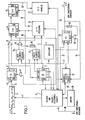
- a time measuring device has a quartz-controlled oscillator 1, which supplies the time base signal with a frequency of, for example, 15 MHz.
- This time base signal is fed via lines 2 to all those circuit parts which are to generate or pass on signals which are synchronized with the time base signal in some way.
- the entire circuit arrangement is from a central computing and sequence control unit 3 according to the requirements of the respective controlled gene measuring task, in the context of which the time measuring device is used.
- the individual signals are fed into the time measuring device according to FIG. 1 via input E. From there they arrive directly at a controllable delay arrangement 5, on whose output line 6 these individual signals with a delay 0 depending on a signal given by the computing and sequence control unit 3 via line 7 to the controllable delay arrangement 5.
- ⁇ O , ie appear without delay or with a delay that is an integer multiple of the unit delay X ".
- An individual signal thus delayed arrives via line 6 at the clock input of a flip-flop 8, which has previously been sent via OR gate 9 either with the aid of a master reset pulse emitted by computing and sequence control unit 3 or with the aid of one from a buffer store Control 10 output reset pulse has been brought into the reset state.
- the Q output of the flip-flop 8 which was previously at logic 0, opens with the rising edge of the individual signal supplied on line 6 logical 1 set.
- the resulting rising edge on the one hand reaches via the OR gate 12 to the start input of a time / amplitude converter circuit 14, which then begins the measurement process, and to a trigger input of the buffer control 10, and on the other hand to the trigger input of a first one Edge enable circuit 15, which receives the time base signal at its second input via line 2 and after triggering by the Q output Signal of the flip-flop 8 counts the rising edges of the time base signal and supplies the fourth edge via the OR gate 16 to the stop input of the time / amplitude converter circuit 14, which thereby stops its measuring operation and maintains the output voltage reached until under the direction of the buffer control 10, this is taken over into a sample-and-hold circuit 17 serving as an analog buffer.
- the sample-and-hold circuit 17 is supplied with a corresponding control signal
- the buffer controller 10 emits a reset signal via the line 19, by means of which the time / amplitude converter circuit 14 and, as already mentioned above, the D flip-flop 8 are reset to their respective initial state, in which they are ready for the processing of the next individual signal coming in via input E.
- the analog measurement result present at the output of the sample-and-hold circuit 17 reaches an analog / digital converter 22 via the line 20, which converts it into a digital form under the direction of the computing and sequence control unit 3 and this digital value to the computing and sequence control unit 3 for further processing via the bidirectional line 923, on which it also receives its control commands.
- the computing and sequence control unit 3 processes the measurement results obtained in this way and the calibration measurement values obtained in a similar manner and calculates the measurement result that is actually of interest, which can be displayed on a display unit 25.
- a D flip-flop 26 is shown, the D input of which is connected to the central computing and sequence control unit 3 via a line 27 given times can be supplied with a logical 1.
- This D flip-flop 26 represents the simplest form of a synchronization circuit, which is provided according to the invention, so that whenever the corresponding preparatory signal has been emitted via the line 27 from the computing and sequence control unit 3, an exact to the time base signal To deliver a defined phase position trigger signal for a generator (not shown in FIG. 1), which thus generates the individual signals that appear later at input E in a strictly phase-locked correlation to the time base signal.
- the time base signal of the oscillator 1 is fed to the clock input of the D flip-flop 26 via the corresponding line 2.
- the preparation signals emitted by the arithmetic and sequence control unit 3 for triggering a synchronized trigger signal are generated at the required time intervals so that the individual signal generator first generates n, ie for example eight individual signals of the first and then n, that is again eight individual signals of the second type .
- the information required for this can again be obtained from the computing and process Control unit 3 are supplied, as indicated by line 30.
- each of these individual signals on the way from the signal generator to the input E of the time measuring circuit is subject to a certain delay, the size of which is unknown, the same for the individual signals of a signal group and generally different from signal group to signal group.
- the corresponding measured values can be obtained with the aid of a counter 32, which transmits this via line 2 Receives time base signal of the oscillator 1 and counts its relevant (ie either the rising or the falling) edges.
- the start of counting of counter 32 is triggered by synchronization flip-flop 26 via line 34.
- the count result can be via the bidirectional lines 33 can be transferred from the counter 32 into the computing and sequence control unit 3.
- the counting operation of the counter 32 for each individual signal is ended by the output signal of the OR gate 16, which also stops the time / amplitude converter circuit.
- this output signal of the OR gate 16 is fed to the arithmetic and sequence control unit 3 in order to indicate that the counting result can now be taken over by the counter 32 on the lines 33.
- a start-stop control 35 is provided, which, depending on whether it is from the computing and sequence control unit 3 at its input E1 or at its input Input E2 a trigger receives signal, can carry out two different calibration measurements.
- the time / amplitude converter circuit 14 Due to this triggering via the input E1 of the start-stop control 35, the time / amplitude converter circuit 14 thus operates for a period that is somewhat longer than three periods of the time base signal and thus provides a first measured value suitable for establishing a calibration line, since yes the period length of the time base signal supplied by the quartz-controlled oscillator 1 is known with very high accuracy and is constant.
- the arithmetic and sequence control unit 3 applies a trigger signal to the input E2 of the start-stop control 35, it generates a start and a stop signal again at its two outputs, but this time this time by exactly one period length of the time base signal are offset from each other. They are supplied in the same way as described above to the time / amplitude converter circuit 14, which in this second type of calibration measurement is for a time space works that is slightly longer than four period lengths of the time base signal.
- a controllable delay arrangement 5 is used in the method according to the invention, of which an embodiment in Fig. 2 is shown in more detail.
- the individual signals appearing at input E are fed to a chain of seven series-connected delay elements 40 to 46, each of which consists of three series-connected AND gates, the two inputs of which are short-circuited to one another.
- the type and the number of delay elements that are selected to form the delay elements 40 to 46 are of minor importance.
- each of the delay elements 40 to 46 delivers approximately the same delay G 0, although deviations of + 30% are entirely tolerable, and that eight times this delay ⁇ O is equal to the time length of the calibrated characteristic range of time / amplitude.
- Converter circuit 14, ie in the present case is approximately equal to a period length of the time base signal.
- controllable delay arrangement 5 comprises eight AND gates 47 to 54, of which the first 47 is connected with its one input to the input of the first delay element 40, the second 48 to the input of the second delay element 41, etc., during the one input of the last AND gate 54 is connected to the output of the last delay element 46.
- the respective second inputs of the AND gates 47 to 54 are connected to the outputs Q 0 to Q 7 of a Johnson counter 56, which always outputs a logical 1 at only one of its Q outputs, while all other Q outputs are at a logical O lie.
- the clock input of the Johnson counter 56 is connected via the line 7 to the central computing and sequence control unit 3, so that the latter can determine which of the Q outputs of the Johnson counter 56 is a logical one by emitting a corresponding number of clock signals 1 to the associated AND gate. This ensures that only one of the AND gates 47 to 54 is open while all the others are blocked.
- this individual signal in the controllable delay arrangement 5 can run through the same signal path as the immediately preceding individual signal from the other signal group, with the Johnson counter 56 in the same position .
- the central computing and sequence control unit 3 Before the next individual signal of the first signal group is then generated on the basis of a trigger signal emitted by the synchronization circuit 26 to the individual signal generator, the central computing and sequence control unit 3 outputs a clock pulse to the Johnson counter 56 via line 7, which then has its Q. 1 output outputs a logic 1, while all other Q outputs are at logic 0 . Then appears the single signal at input E, so. it cannot reach the OR gate 57 via the output of the now blocked AND gate 47. Rather, it must pass through the first delay element 40, whereupon it is passed on from the now open AND gate 48 to the OR gate 57 and from there to the D flip-flop 8. Thus, this individual signal has been delayed by the controllable delay arrangement 5 by a time ⁇ O.
- each subsequent individual signal / delay can then be subjected to a delay that is greater by ⁇ O than the delay of the previous individual signal.
- the maximum delay value that can be achieved in this way is 7. ⁇ O , which is reached when the Johnson counter has a logic 1 at its output Q 7 .
- n / signal groups comprising eight individual signals which are nested within one another can be generated.
- the Johnson counter 56 is clocked further by a further clock signal appearing on line 7, so that a logic 1 appears at its output Q 8 , through which it resets itself to its initial state, in which at the output Q a logical 1 is available.
- the Johnson counter 56 is now ready for the next signal group.
- FIG 3 shows the first and second edge enable circuits 15 and 37, the start / stop control 35 providing the calibration start / stop signals and the delay element 38 connected downstream of the second edge enable circuit 37 in greater detail.
- FIG. 3 shows the D flip-flop 8, which receives the individual signals on line 6 after they have passed through the controllable delay arrangement 5. If such an individual signal arrives at the clock input of the D flip-flop 8, then this is set by the rising edge of the individual signal, as a result of which a logic 1 appears at its Q output, which, as already mentioned, via the OR gate 12 as Start signal is passed to the time / amplitude converter circuit.
- this logic 1 is fed to the data input of a D flip-flop 58, which forms the input stage of a first edge enable circuit 15, which consists of a flip-flop chain comprising a total of four D flip-flops 58 to 61, where the Q output of a preceding flip-flop is connected to the D input of a subsequent flip-flop.
- the clock inputs of all of these flip-flops 58 to 61 are supplied with the 15 MHz time base signal via line 2.
- the D flip-flop 58 forming the input stage of this first edge enable circuit 15 has a certain response delay, i.e. a certain minimum period of time must elapse between the application of logic 1 to the D input of this flip-flop and the appearance of the next clock signal edge, so that logic 1 is actually transferred to the Q output by this edge.
- the individual signals triggering the D flip-flop 8 have been generated in such a way that they have a fixed temporal correlation to the time base signal. Between their generation and their entry into the time measuring device, however, they experience a delay of unknown size, which is to be measured by the time measuring method according to the invention.
- This unknown delay can easily assume such a value that either the undelayed passing through the delay arrangement 5 or one of the additionally delayed individual signals triggers the D flip-flop 8 so shortly before the occurrence of the next rising edge of the time base signal that the flip-flop Flop 58 no longer responds to this rising edge due to its response delay described above, so that the flip-flop 61 only outputs a stop signal to the time / amplitude converter circuit 14 when the fifth signal edge occurs.
- the time / amplitude converter circuit then operates somewhat longer than four periods of the time base signal.
- start-stop control 35 is reproduced in detail, which the central computer and sequence control unit 3 receives a trigger signal either at its input E1 or at its input E2 and then initiates either a calibration measurement of the first type or a calibration measurement of the second type.
- an OR gate 63 connected to these two inputs also outputs a logic 0 at its output, which corresponds to the D input Flip-flops 64 is supplied. Since the clock input of this flip-flop 64 is connected to the time base signal, this logic O is also maintained at this status of the inputs E1 and E2 at the Q output of the flip-flop 64, from where it on the one hand to the data input of another flip-flop 65 and to the one input of an AND gate 66.
- the Q output of flip-flop 64 which is simultaneously at logic 1, is connected to the reset input of flip-flop 65, which is kept in its reset state by this logic level, so that a logic 0 also appears at its Q output , which is led to the one input of a further AND gate 67 and the D input of a third flip-flop 68, the reset input of which is also connected to the Q output of flip-flop 64, so that the Q output of the flip-flop 68, which is also the start output of the start-stop controller 35, has a logic 0 which is led to the second input of the OR gate 12.
- the two AND gates 66 and 67 each receive a logical 0 at both inputs in this state, in which no trigger signal has yet been applied to the inputs E1 or E2, they also output a logical 0 at their respective outputs, so that the OR gate connected downstream of them also shows a logic 0 at its output, which is fed to the D input of a fourth flip-flop 70, the reset input of which is also connected to the Q output of flip-flop 64 is bound, so that the flip-flop 70 is held in its reset state, inaem at its Q output a logic 0 appears, which is passed on to the D input of a fifth flip-flop 71, the reset input of which is also connected to the Q output of flip-flop 64 is connected, so that this flip-flop 71 is also reset.
- the Q output of the flip-flop 71 which is at logic O at this stage, is the stop output of the start-stop controller 35.
- the clock inputs of the flip-flops 65, 68, 70 and 71 are also on the line carrying the time base signal 2 connected.
- the central computing and sequence control unit 3 now applies a positive trigger signal to the input E1 of the start-stop control 35 to carry out a calibration operation of the first type, the logical 1 level associated therewith on the one hand reaches the OR gate 63 to the D input of the flip-flop 64 and on the other hand to the one of the two inputs of the AND gate 66.
- This logic 1 level is maintained by the central computing and sequence control unit 3 for a longer period of time.
- the logic 1 present at the data input of the flip-flop 64 can first be transmitted to the Q output by the first rising edge of the time base signal following the application of the trigger signal. From there it arrives on the one hand at the data input of the flip-flop 65 and on the other hand via the AND gate 66, which now has a logic 1 at its two inputs, and the OR gate 69 at the data input of the flip-flop 70.
- the third rising edge of the time base signal following the application of the trigger signal then also sets the two flip-flops 68 and 71 at the same time, so that the Q-outputs connected to the start or stop output of the start-stop Control 35 are identical, two rising edges appear at the same time, one of which reaches the time / amplitude converter circuit 14 as a start signal via the OR gate 12, while the logical 1- appearing at the stop output of the start-stop controller 35 Level is applied to the input of a second edge enable circuit 37, which, like the first edge enable circuit 15, is constructed from a chain of D flip-flops 75, 76 and 77, each of which has the Q output a preceding flip-flop is connected to the D input of a subsequent flip-flop and in which all clock inputs are connected to line 2 carrying the time base signal.
- a second edge enable circuit 37 which, like the first edge enable circuit 15, is constructed from a chain of D flip-flops 75, 76 and 77, each of which has the Q output a preceding flip-flop is connected
- this second edge enable circuit comprises only three flip-flops, the third rising edge of the time base signal of the Q-, which occurs after the simultaneous appearance of the start and stop signals at the relevant outputs of the start-stop controller 35, Output of the last flip-flop 77 of this chain is set to logic 1.
- the rising edge that occurs is caused by the delay element 38 connected downstream of this output, which in the present case consists of three series-connected elements and their inputs short-circuited gates is delayed by a time equal to the response delay of the input flip-flop 58 of the first edge enable circuit 15 and then supplied via the OR gate 16 to the time / amplitude converter circuit 14 as a stop signal. So thus operates the time / amplitude converter circuit 14 in this calibration - process the first type for a period of time to the slight delay of the delay element 38 for more than three period lengths of the time base signal.
- the computing and sequence control unit 3 If this calibration measurement of the first type is completed, the computing and sequence control unit 3 generates a master reset signal, by means of which the flip-flop 64 is reset. Since logic 1 is no longer present at input E1, flip-flop 64 remains reset. As a result of the logic 1 occurring at its Q output when reset, the other flip-flops 65, 68, 70 and 71 are also forcibly reset, provided that this has not already been done by shifting logic 0 levels. The start and the stop output of the start-stop control 35 are thus logic 0 again.
- the computing and sequence control unit 3 supplies a corresponding trigger signal to the input E2.
- the processes then taking place as a function of the rising edges of the time base signal largely correspond to the processes described above for the first type of calibration measurement.
- the data input of the flip-flop 70 receives its logic 1 not at the same time as the data input of the flip-flop 65, but only at the same time as the data input of the flip-flop 68, since in the present case the AND gate 66 is blocked via the input E1 and the AND gate 67 opened via the input E2 is connected with its second input to the Q output of the flip-flop 65.
- This has the effect that the start signal for the time / amplitude converter circuit 14 at the Q output of the flip-flop 68 appears earlier than the stop signal at the Q output of the flip-flop 71 by a period length of the time base signal.
- this stop signal is then also shifted again by the edge enable circuit 37 by three period lengths and delayed by the delay element 38 in the same way as the stop signal in the calibration measurement of the first type, the time / Amplitude converter circuit for a period that is slightly greater than four period lengths of the time base signal.
- the time / amplitude converter circuit when performing the time interval measurements for the individual signals also works for a period of time that is at least equal to three and at most equal to slightly more than four period lengths of the time base signal, it is thus ensured that the Measured values obtained thereby always fall within the calibrated characteristic curve range of the time / amplitude converter circuit lying between the two calibration measuring points.
- the time base signal generated by the oscillator 1 is shown in the top line as a square-wave signal, the period length of which is denoted by T.
- T the period length of which is denoted by T.
- a single signal appearing at input E not the entire pulse reproduced in this second line, but only its rising edge 80 representing the single signal whose time interval from a defined subsequent edge, in the present case to edge 81 of the time base signal, is measured should.
- the flip-flop 8 is set by the edge 80, so that its Q output, as shown in the third line from the top of FIG. 4, jumps to a logic 1 level.
- the rising edge 82 ′ which occurs in this case starts the time / amplitude converter circuit via the OR gate 12, while the logic 1 level which follows the edge 82 prepares the edge enable circuit 15 for counting the subsequent rising edges of the time base signal.
- This is indicated in the fourth line from the top of FIG. 4 with the Q output signal of flip-flop 58, which goes to logic 1 when the first rising edge 83 of the time base signal follows the individual signal edge 80.
- This logic 1 is then pushed on by the flip-flop chain 59, 60, 61 with each rising edge of the time base signal, so that when the fourth edge 81 of the time base signal occurs, the Q output of the last flip-flop 61 of this chain is logic 1 goes.
- the rising edge 84 which occurs in this case is supplied via the OR gate 16 to the time / amplitude converter circuit as a stop signal.
- a typical output characteristic of a time / amplitude converter circuit 14 is shown below these pulse diagrams.
- Such a circuit essentially consists of a charging capacitor which is discharged via a switch which is parallel to it and is closed in the idle state, so that in the idle state the two capacitor plates are at the same voltage, namely at the supply voltage U 0 of the time / amplitude converter circuit 14.
- a constant current source that can be switched on and off, which consists of a sufficiently fast switchable GHz transistor and an emitter resistor designed according to the desired size of the current impression.
- the time / amplitude converter circuit 14 occurs after a start
- the calibrated range of the characteristic is designated in FIG. 4 by the points 9 and 91 0.
- the front point 90 obtained by a calibration measurement of the first type has a distance of 3 from the switch-on time t O of the time / amplitude converter circuit 14.
- T + ⁇ t where A t means the delay introduced by the delay element 38.
- point 91 obtained by a second type of calibration measurement is at a distance of 4 from time t 0 .
- T + ⁇ t A calibration line 92 is placed between these two calibration points 90 and 91, and it can clearly be seen that the actual characteristic curve deviates considerably from the ideal curve 92 due to the non-linearities present.
- the associated switch-off edge 84 ' will generally be located at a different point in the calibrated characteristic curve area, at which a another F volun- t2'- t1 'results, so that the error t2-t1 and t2 during the subsequent subtraction of these two measured time' ler - t1 'not lift sufficiently with each other.
- the method according to the invention ensures that the repetition of the respective individual signals and the shifting of the switch-off flank 84 with the aid of the different delays of the individual signals over the entire calibrated characteristic curve range ensures that all errors possible due to the nonlinear functionality in the / mean value of a signal group about the same amount. Since this applies to both signal groups, the mean values of which are subsequently subtracted from one another, these error sums cancel each other out almost or completely.
- a preferred buffer control 10 comprises a frequency divider arrangement which consists of a flip-flop 80, a 10: 1 divider 81 connected with its counting input to the Q output of the flip-flop 80 and consists of a 4-bit binary counter 82 connected with its counting input to the counting output of the 10: 1 divider 81, the 15 MHz time base signal of the oscillator 1 being supplied to the clock input of the flip-flop 80.
- the Q output of this flip-flop 80 is connected to the D input of this flip-flop, so that the flip-flop 80 permanently outputs square-wave signals with a repetition frequency of 7.5 MHz at its Q output.
- the output signals of the frequency divider arrangement are decoded with the aid of AND gates in order to generate a track-hold signal of suitable length for the sample-and-hold circuit 17 at suitable times, as will be explained below.
- a "hold" signal i.e. in the present case there is a logical zero.
- this logic zero is output by an AND gate 85, the input of which is supplied with a logic zero by the Q output of a flip-flop 86, since the flip-flop 86 via the OR gate 87 has been reset by a previous master reset pulse emitted by the central computing and sequence control unit 3 or by a reset pulse generated by the buffer controller 10 itself.
- the other input of the AND gate 85 is connected to the output of an inverter 88 which supplies a logic one in the considered idle state, since the AND gate 89 which drives the input of the inverter 88 receives a logic zero at its two inputs and thus on outputs a logical zero at its output.
- AND gate 89 One input of AND gate 89 is connected to the Q D output of 4-bit binary counter 82, while the other input of AND gate 89 is connected to the output of a further AND gate 90, the inputs of which are connected to the Q B - or Q A output of the 4-bit binary counter 82 are connected. Since this counter 82 is kept in the reset state in the considered idle state via its reset input. its outputs Q A to Q D each have a logic zero, which leads via AND gates 90 and 89 to the drive state for inverter 88 described above.
- the 10: 1 divider 81 is also forced in the idle state of the buffer control 10 via its reset input. held in the reset state so that a logical zero is also present at its outputs Q to Q D.
- the outputs Q A and Q D of the 10: 1 divider 81 are connected to the two inputs of an AND gate 91, the output of which is connected to the clock input of the flip-flop 86. Since a logic zero is supplied to the two inputs of the AND gate 91 in the period under consideration, its output is also at a logic zero, so that the flip-flop 86 is not activated.
- the 1 level holding the 10: 1 divider 81 and the 4-bit binary counter 82 in the reset state is supplied by an OR gate 92, one input of which is connected via a delay element 93 to the output of an AND gate 94, which supplies a logic zero because its one input is connected to the logic zero-providing Q C output of the 10: 1 divider 81 and its other input is connected to the logic-zero output of the AND gate 89.
- the second input of the OR gate 92 is connected to the Q output of a flip-flop 95 which, via an OR gate 96 which drives its reset input, either with the aid of a previous master reset pulse or via one of the latch control 10 self-generated reset pulse has been reset so that its Q output provides the logic 1 which is passed from the OR gate 92 to the reset inputs of the 10: 1 divider 81 and the 4-bit binary counter 82.
- the clock input of the flip-flop 95 is connected to the output of the OR gate 12, which is also connected to the start input of the time / amplitude converter circuit 14.
- the flip-flop 95 is also set by this rising edge, since its D input is always at logic 1. This setting of the flip-flop 95 causes the buffer control 10 to start, since after the time / amplitude converter circuit 14 has started, a new measured value is to be expected at its output, with a certain delay, which is in the sample-and-hold Circuit 17 must be taken over.
- This delay is generated with the aid of the frequency divider arrangement 80, 81 and 82, which is initiated in that the reset inputs of the 10: 1 divider 81 and the 4-bit binary counter 82 are enabled by the application of a logic 0.
- This logic 0 arises from the fact that when the flip-flop 95 is reset, its Q output switches to logic 0 and thus a logic 0 is present at both inputs of the OR gate 92.
- the 10: 1 divider 81 is enabled to react to the 7.5 MHz pulses present at its counting input and output by the flip-flop 80.
- a logical 1 appears simultaneously on the Q A and Q D outputs of the 10: 1 divider 81, so that also the AND gate 91 switches from logic O to logic 1 at its output.
- the resulting positive edge sets the flip-flop 86, whose D input is always at logic 1.
- a logic 1 appears at the Q output of the flip-flop 86 and is applied to the control input of the sample-and-hold circuit 17 via the AND gate 85, at the other input of which the logic 1 output by the inverter 88 is present "Track" signal is emitted so that it begins to take over the measured value present at the output of the time / amplitude converter circuit 14.
- "Track" signal is emitted so that it begins to take over the measured value present at the output of the time / amplitude converter circuit 14.
- There is a certain minimum period of time for this transfer which essentially takes place in that a capacitor contained in the sample-and-hold circuit 17 is charged via a finite resistor to the same voltage that is present at the output of the time / amplitude converter circuit 14 required, which is determined by the time constant of the charging capacitor in question and the associated charging resistance.
- a track signal of sufficient length is generated in that the 4-bit binary counter 82 only at its Q A - ' Q B at the eleventh output pulse of the 10: 1 divider 81, ie only after 220 periods of the 15 MHz time base signal - and Q D output produces a logic 1, which is passed via the AND gates 90 and 89 to the input of the inverter 88, which then applies a logic 0 to the corresponding input of the AND gate 85, so that the output of the AND -Gatters 85 appearing control signal for the Sam p le-and-hold circuit 17 drops to the "hold" level.
- the timing of the falling edge which lays down the cached by the sample-and-H old-circuit inherited and for the subsequent digitization voltage value is about the frequency divider arrangement 80, 81, 82 and the AND gates 90, 89, the inverter 88 and the AND gate 85 correlates exactly with the 15 MHz time base signal. Although there is a certain time delay between the mentioned falling edge and the associated rising edge of the 15 MHz time base signal, this delay can, with very good approximation, be regarded as constant, at least in the short period of time required to separate them to subtract measured values of two individual signal groups.
- This time synchronization of the falling edge appearing at the output of the AND gate 85 with the time base signal ensures that interference voltages originating from this time base signal are superimposed on the output signal of the time / amplitude converter circuit 14 and therefore by the sample and hold Circuit 17 are taken over, go into each measured value with the same amplitude and are therefore eliminated in the subsequent subtraction.
- the logic 1 appearing at the output of the AND gate 89 is also connected via the OR gate 87 to the reset input of the flip-flop 86, which is thereby reset.
- the logical 0 that appears at its Q output initially has no effect, since the AND gate 85 also receives a logical 0 at its other input.
- the logic 1 present at the output of the AND gate 89 is initially suppressed by the AND gate 94 until the Q C output of the 10: 1 divider 81 outputs a logic 1 for the first time after the processes just described. This is the case after a further eight periods of the 15 MHz time base signal and since it is ensured by the reset flip-flop 86 that the logic 0 present at the output of the AND gate 85 is held, can now be achieved by the AND gate 94 Output logic 1 of the 10: 1 divider 81 and the 4-bit binary counter 82 are reset via the OR gate 92.
- the delay element 93 ensures that this reset signal, which also brings the flip-flop 95 into the idle state via the OR gate 96, has a sufficient length.
- controllable switches of the controllable delay arrangement 5 formed by AND gates 47 to 54 in the exemplary embodiment according to FIG. 2 can advantageously also be implemented with relays. Relays with a guaranteed number of operating cycles of 10 9 are available, which guarantees a sufficient service life.
- a major advantage of this arrangement is that there is complete potential isolation, so that no reflections on in principle switched off but not completely separated Circuit parts can occur.
- AND gates are used as controllable switches, these reflections have the consequence that the individual delay elements deliver different delay values, depending on their position within the delay chain, with signal propagation times that are basically the same per se.
Abstract
Bekannte Zeitmeßverfahren verwenden zur Berechnung eines Meßwertes die Differenz von Zeitabständen, die zwei zwischen ihrer Erzeugung und der Zeitmessung unterschiedliche Verzögerungen erleidende, wiederholbare Einzelsignale von einer jeweils zugehörigen Zeitbasissignalflanke aufweisen. Diese Zeitabstände werden mit derselben Zeit/Amplituden-Wandlerschaltung gemessen, deren Kennlinie einen geeichten, wenigstens einer Periodenlänge des Zeitbasissignals entsprechenden, durch lineare Interpolation zwischen zwei Eichmeßpunkten gebildeten Bereich umfaßt. Zur Vermeidung von Meßfehlern, die aufgrund von Nichtlinearitäten der tatsächlichen Kennlinie im geeichten Bereich entstehen können, wird erfindungsgemäß jedes der beiden Einzelsignale n-mal phasenstarr zum Zeitbasissignal erzeugt und der Zeit/Amplituden-Wandlerschaltung jeweils einmal unmittelbar und n-1-mal mit jeweils einer anderen zusätzlichen Verzögerung zugeführt, wobei die Verzögerungswerte so gewählt werden, daß sie in etwa jeweils ein ganzzahliges Vielfaches einer Einheitsverzögerung τ0 sind und n . τ0 gleich der Periodenlänge der Zeitbasissignals ist. Zur Meßwertbildung wird dann die gemittelte Differenz der für die beiden Signalgruppen gewonnenen Ausgangssignalwerte der Zeit/Amplituden-Wandlerschaltung verwendet.Known time measurement methods use the difference of time intervals for calculating a measured value, which have two repeatable individual signals which suffer different delays between their generation and the time measurement from a respectively associated time base signal edge. These time intervals are measured with the same time / amplitude converter circuit, the characteristic curve of which comprises a calibrated area which is formed by linear interpolation between two calibration measuring points and corresponds to at least one period length of the time base signal. In order to avoid measurement errors that may arise in the calibrated range due to non-linearities of the actual characteristic curve, each of the two individual signals is generated n times phase-locked to the time base signal according to the invention and the time / amplitude converter circuit each once and n-1 times with one each fed to another additional delay, the delay values being chosen such that they are approximately an integer multiple of a unit delay τ0 and n. τ0 is equal to the period length of the time base signal. The averaged difference between the output signal values of the time / amplitude converter circuit obtained for the two signal groups is then used to form the measured value.
Description
Die Erfindung betrifft ein Zeitmeßverfahren gemäß dem Oberbegriff von Anspruch 1.The invention relates to a time measurement method according to the preamble of
Bei einem derartigen, beispielsweise aus der DE-OS 30 12 186 bekannten Zeitmeßverfahren sind die beiden wiederholbaren Einzelsignale zwei Zeitmarkensignale, deren zeitlicher Ab-stand möglichst genau bestimmt werden soll. Der betreffende Meßwert wird nicht unmittelbar, sondern rechnerisch aus drei Einzelmeßwerten, einem sogenannten Grobmeßwert und zwei sogenannten Feinmeßwerten gewonnen. Dabei ergibt sich der Grobmeßwert durch Abzählung der zwischen den beiden Zeitmarkensignalen aufgetretenen Perioden eines Zeitbasissignals, das von einem freilaufenden, d.h. mit den beiden Zeitmarkensignalen in keiner Weise korrelierten oder synchronisierten quarzgesteuerten Oszillator geliefert wird. Die beiden Feinmeßwerte, die jeweils den zeitlichen Abstand des früheren bzw. späteren Zeitmarkensiqnals zu einer nachfolgenden, z.B. zur nächsten steigenden Flanke des Zeitbasissignals angeben, werden mit Hilfe ein und derselben Zeit/Amplituden-Wandlerschaltung auf analogem Wege gemessen und nach einer erfolgten Analog/Digital-Wandlung mit dem Grobmeßwert zur Berechnung des interessierenden Gesamtmeßwertes vorzeichenrichtig. kombiniert. Im Normalfall bedeutet dies, daß der eine der beiden Feinmeßwerte zum Grobmeßwert addiert und der andere vom Grobmeßwert subtrahiert wird, so daß insgesamt die Differenz der .beiden Feinmeßwerte, d.h. also der Zeitabstände, die das erste und das zweite wiederholbare Einzelsignal von einer definierten Flanke des periodischen Zeitbasissignals aufweisen, in das eigentlich interessierende Meßergebnis eingeht. Dabei können statt der steigenden auch die fallenden Flanken des rechteckförmigen Zeitbasissignals oder entsprechende Nulldurchgänge eines sinusförmigen Zeitbasissignals als Bezugspunkte dienen.In such, for example, from DE-OS 30 12 186 are known, the two time measuring repeatable individual signals two time marker signals whose temporal b A-stand is to be determined as precisely as possible. The measured value in question is not obtained directly, but arithmetically from three individual measured values, a so-called rough measurement value and two so-called fine measurement values. The coarse measurement value is obtained by counting the periods of a time base signal that occurred between the two time mark signals, which is supplied by a free-running, ie crystal-controlled oscillator that is in no way correlated or synchronized with the two time mark signals. The two fine measurement values, which each indicate the time interval between the earlier or later time mark signal to a subsequent, e.g. to the next rising edge of the time base signal, are measured using the same time / amplitude converter circuit in an analog way and after an analog / digital has taken place - Conversion with the rough measurement value to calculate the total measurement value of interest with correct sign. combined. Normally this means that one of the two fine measurement values is added to the coarse measurement value and the other is subtracted from the coarse measurement value, so that the difference between the two fine measurement values, i.e. the time intervals between the first and the second repeatable individual signal from a defined edge of the have periodic time base signal, into the actually interesting measurement result. Instead of the rising edges, the falling edges of the rectangular time base signal or corresponding zero crossings of a sinusoidal time base signal can also serve as reference points.
Ein typisches Anwendungsbeispiel für dieses bekannte Zeitmeßverfahren stellen beispielsweise Entfernungsmeßverfahren nach dem Prinzip der Laufzeitmessung eines Lichtimpulses dar, bei denen der von einer Sende-Lichtquelle emittierte Lichtimpuls innerhalb des Meßgerätes in einen Meßlichtimpuls und einen Referenzlichtimpuls aufgeteilt wird, wobei ersterer über die Sendeoptik zum Zielgegenstand emittiert, von dort zum Meßgerät reflektiert und im Meßgerät auf einen Lichtempfänger geleitet wird, der zuvor über einen kurzen, geräteinternen Referenzlichtweg bekannter Länge den Referenzlichtimpuls erhalten hat. Beide Lichtimpulse lösen in der dem Lichtempfänger folgenden Auswerteschaltung zwei Signale aus, die die Zeitmarkensignale des oben beschriebenen Zeitmeßverfahrens darstellen und deren zeitlicher Abstand ein Maß für die Entfernung des Zielgegenstandes ist. Wegen der normalerweise unterschiedlichen Länge des Referenzlichtweges und des Meßlichtweges unterliegt jedes dieser beiden zunächst gleichzeitig erzeugten Einzelsignale einer eigenen Verzögerung, die sich von der des anderen Signals unterscheidet. Solange sich jedoch die Entfernung zwischen dem Zielgegenstand und dem Entfernungsmeßgerät nicht ändert, bleiben auch die Verzögerungen dieser beiden Signale bei einer wiederholten Lichtimpuls-Erzeugung unverändert.A typical application example for this known time measurement method is represented, for example, by distance measurement methods based on the principle of time-of-flight measurement of a light pulse, in which the light pulse emitted by a transmitter light source is divided within the measuring device into a measurement light pulse and a reference light pulse, the former emitting to the target object via the transmitter optics, from there it is reflected to the measuring device and is passed in the measuring device to a light receiver which has previously received the reference light pulse via a short, internal reference light path of known length. Both light pulses trigger two signals in the evaluation circuit following the light receiver, which represent the time stamp signals of the time measurement method described above and whose time interval is a measure of the distance of the target object. Because of the normally different lengths of the reference light path and the measurement light path, each of these two individual signals initially generated at the same time is subject to its own delay, which differs from that of the other signal. However, as long as the distance between the target object and the distance measuring device does not change, the delays of these two signals also remain unchanged when the light pulse is generated again.
Eine andere Anwendungsmöglichkeit für ein Zeitmeßverfahren gemäß dem Oberbegriff des Anspruchs 1 stellt die Messung der Phasenverschiebung zwischen zwei periodischen Signalen derselben Frequenz dar. Nimmt man beispielsweise an, daß es sich dabei um periodische Rechtecksignale handelt, so sind zwei innerhalb einer Periodenlänge aufeinanderfolgende stei- fende Flanken des einen und des anderen periodischen Signals die wiederholbaren Einzelsignale und die Phasenverschiebung zwischen den beiden periodischen Signalen kann dadurch gemessen werden, daß man die Zeitabstände dieser wiederholbaren Einzelsignale zu einer nachfolgenden definierten, beispielsweise der nächsten steigenden Flanke eines dieselbe Frequenz besitzenden Zeitbasissignals mißt, wobei dann wieder die Differenz dieser beiden Zeitabstände in das interessierende Meßergebnis eingeht. Der wesentliche Unterschied zu dem aus der DE-OS 30 12 186.9 bekannten Zeitmeßverfahren besteht hier darin, daß nur die beiden sogenannten Feinmeßwerte, nicht aber ein Grobmeßwert ermittelt werden. Die Summe der unterschiedlichen Verzögerungen, denen die beiden wiederholbaren Einzelsignale vor der Zeitmessung unterworfen sind, ergibt die zu messende Phasenverschiebung. Dabei müssen diese beiden Verzögerungen nicht dadurch entstanden sein, daß die beiden durch die periodische Wiederholung der Einzelsignale entstehenden Signale gleichzeitig, d.h. ohne Phasenverschiebung erzeugt worden sind und dann Wege unterschiedlicher'Länge durchlaufen haben. Stattdessen können die unterschiedlichen Verzögerungen den beiden periodischen Signalen auch von Anfang an, d.h. bereits bei ihrer Erzeugung aufgeprägt sein.Another application for a time measuring method according to the preamble of
Darüber hinaus sind noch weitere Anwendungsfälle für Zeitmeßverfahren gemäß dem Oberbegriff des Anspruches 1 denkbar, denen jedoch allen gemeinsam ist, daß zwei im allgemeinen unterschiedliche Zeitabstände; die ein erstes und ein zweites wiederholbares Einzelsiqnal von einer definierten nach- steigenden(oder fallenden) folgenden oder vorausgehenden/Flanke eines rechteckförmigen Zeitbasissignals oder einem nachfolgenden oder vorausgehenden definierten Nulldurchgang eines sinusförmigen Zeitbasis- signals aufweisen, gemessen und ihre Differenz zur Gewinnung eines weiteren Meßwertes verarbeitet werden soll. Dabei wird vorausgesetzt, daß die Differenz zwischen dem Zeitabstand des ersten und dem /Zeitabstand des zweiten Einzelsignals zu dem entsprechenden Punkt des Zeitbasissignals bei den Wiederholungen dieser Einzelsignale unverändert bleibt. Gemessen werden die Zeitabstände mit ein und derselben Zeit/Amplituden-Wandlerschaltung, wobei dann, wenn die voneinander zu subtrahierenden Meßwerte genügend rasch hintereinander gewonnen werden, nicht nur lang- und mittelfristige Drifterscheinungen, sondern auch kurzfristige Schwankungen durch die Differenzbildung herausfallen. Dabei ist es allerdings erforderlich, zur Beseitigung von Schwankungs- und Drifterscheinungen des Kennlinienverlaufs der Zeit/Amplituden-Wandlerschaltung diese Schaltung ständig mit Hilfe eines Eichnormals nachzueichen, wozu sich beispielsweise dann, wenn das Zeitbasissignal mit Hilfe eines quarzgesteuerten Oszillators erzeugt wird, die Periodenlänge des Zeitbasissignals gut eignet. Allerdings können damit nur einzelne Punkte der Zeit/Amplituden-Wandlerschaltungs-Kennlinie erfaßt werden, die jeweils genau um eine Periodenlänge des Zeitbasissignals voneinander beabstandet liegen. Die zwischen diesen Punkten befindlichen Kennlinienbereiche, die deswegen von besonderer Bedeutung sind, weil die auszumessenden Zeitabstände im Regelfall kein ganzzahliges Vielfaches der Periodenlänge des Zeitbasissignals darstellen, werden dabei
durch eine einfache lineare Interpolation zwischen den Eichmeßpunkten überbrückt.In addition, other applications for time measurement methods are conceivable according to the preamble of
bridged by a simple linear interpolation between the calibration measuring points.
Dabei ergibt sich das Problem, daß die Kennlinie der Zeit/ Amplituden-Wandlerschaltung zwischen den Eich-Meßpunkten so starke Nichtlinearitäten aufweisen kann, daß es bei der Messung der Zeitabstände von zwei Einzelsignalen mit nachfolgender Differenzbildung zumindest dann, wenn eine sehr hohe Genauigkeit verlangt wird, zu unerlaubt großen Fehlern kommen kann, da die beiden Meßwerte im allgemeinen an verschieder Kennlinie denen Stellen/der Zeit/Amplituden-Wandlerschaltung liegen, so daß sie unterschiedliche und sich damit bei der Subtraktion nicht mehr gegenseitig aufhebende, durch die Nichtlinearität der Kennlinie bedingte Fehleranteile enthalten.The problem arises here that the characteristic of the time / amplitude converter circuit between the calibration measuring points can have such strong nonlinearities that when measuring the time intervals of two individual signals with subsequent difference formation, at least when very high accuracy is required, Unauthorized errors can occur, since the two measured values generally lie at different points on the points / time / amplitude converter circuit, so that they contain different parts of the error that are no longer mutually exclusive due to the non-linearity of the characteristic .
Eine Möglichkeit zur Verringerung dieser Fehler besteht darin, die beiden Einzelsignale in mit dem Zeitbasissignal völlig unkorrelierter Weise so häufig zu wiederholen, daß der sich bei einer nachfolgenden Mittelwertbildung ergebende Fehler des Mittelwertes nach dem Wurzelgesetz der Fehlertheorie unter die geforderte Genauigkeitsgrenze absinkt. Bei sehr starken Nichtlinearitäten der Kennlinie der Zeit/Amplituden-Wandlerschaltung bzw. bei einer sehr hohen geforderten Meßgenauigkeit kann hierfür allerdings eine außerordentlich große Anzahl von Wiederholungen der Einzelsignale erforderlich sein, was dazu führt, daß der Zeitraum, der zur Gewin- nung eines entsprechend genauen End-Meßergebnisses erforderlich ist, sehr lang wird. Insbesondere bei Entfernungsmeßverfahren, bei denen die Entfernung von sich schnell bewegenden Gegenständen gemessen werden soll, steht ein solcher langer Meßzeitraum nicht zur Verfügung, da sich ja während die Differenz dieses Zeitraumes/ der Abstände der Einzelsignale von den definierten Punkten des Zeitbasissignals nicht verändern darf.One way of reducing these errors is to repeat the two individual signals so often in a way that is completely uncorrelated with the time base signal that the error of the mean value that results from a subsequent averaging falls below the required accuracy limit according to the root law of error theory. In the case of very strong non-linearities in the characteristic of the time / amplitude converter circuit or in the case of a very high required measuring accuracy, however, this can be an extraordinary its large number of repetitions of the individual signals required, which results in the period of planning for G ewin- is a correspondingly accurate final measurement result required is very long. Such a long measuring period is not available, in particular in distance measuring methods in which the distance of rapidly moving objects is to be measured, since the difference between this period / the distances of the individual signals from the defined points of the time base signal must not change.
Demgegenüber liegt der Erfindung die Aufgabe zugrunde, ein Verfahren der eingangs genannten Art so weiterzubilden, daß trotz des Vorhandenseins unbekannter Nichtlinearitäten der Kennlinie der Zeit/Amplituden-Wandlerschaltung Meßergebnisse mit sehr hoher Genauigkeit innerhalb sehr kurzer Zeiträume gewonnen werden können.In contrast, the invention has for its object to develop a method of the type mentioned so that despite the presence of unknown non-linearities of the characteristic of the time / amplitude converter circuit, measurement results can be obtained with very high accuracy within very short periods of time.
Zur Lösung dieser Aufgabe sieht die Erfindung die im Anspruch 1 niedergelegten Merkmale vor.To achieve this object, the invention provides the features set out in
Durch die erfindungsgemäßen Maßnahmen werden ähnlich wie bei der oben erwähnten statistischen Lösungsmöglichkeit die durch die Nichtlinearitäten der Kennlinie der Zeit/Amplituden-Wandlerschaltung bedingten, bei Einzelmessungen auftretenden, untolerierbar großen Meßfehler dadurch in der erforderlichen Weise verkleinert, daß mehrere, nämlich n Messungen für jedes der beiden Einzelsignale durchgeführt und aus den Meßergebnissen Mittelwerte gebildet werden. Anders als bei der statistischen Fehlerverringerung, die ja nur dann wirksam wird, wenn das Zeitbasissignal mit den Einzelsignalen in keiner Weise korreliert ist, so daß sich bei jeder Einzelmessung andere, in ihrer Größe statistisch verteilte und somit auch mit Fehlern unterschiedlicher Größe behaftete Meßwerte ergeben, wird bei dem erfindungsgemäßen Verfahren für eine Kopplung zwischen der Erzeugung der Einzelsignale und dem Zeitbasissignal gesorgt. Ohne weitere Maßnahmen würde dies zur Folge haben, daß bei jeder Wiederholung eines Einzelsignals derselbe Zeitabstandswert gemessen würde, der auch immer mit demselben Nichtlinearitätsfehler behaftet wäre, so daß sich hierdurch noch keine Steigerung der Meßgenauigkeit ergeben könnte. Dadurch aber, daß gemäß der Erfindung das jeweilige Einzelsignal der Zeit/Amplituden-Wandlerschaltung nur einmal "unverzögert", d.h. ohne zu der "natürlicherweise", z.B. aufgrund einer Signallaufzeit vorhandenen Verzögerung hinzukommende wesentliche weitere Verzögerung, bei jeder der n-1 weiteren Wiederholungen aber gezielt zusätzlich verzögert wird, wobei der Wert dieser zusätzlichen Verzögerung bei jeder Wiederholung ein anderer ist, erhält man bei jeder Messung ein und desselben Einzelsignals einen anderen Meßwert, der dann auch mit einem anderen Nichtlinearitätsfehler behaftet ist. Durch geeignete Wahl der einzelnen n-1 Verzögerungswerte wird erfindungsgemäß dafür gesorgt, daß für ein Einzelsignal n Meßwerte erhalten gesamten werden, die gleichmäßig, d.h. in etwa äquidistant über den/ geeichten Kennlinienbereich der Zeit/Amplituden-Wändlerschaltung verteilt sind, so daß alle durch die Nichtlinearität der Zeit/Amplituden-Wandlerschaltungs-Kennlinie möglichen Fehlerbeiträge in etwa gleichmäßig erfaßt werden. Da dasselbe dann auch bei den n Einzelsignalen der anderen Signalgruppe geschieht, wobei jeder der n-1 verschiedenen, bei der ersten Signalgruppe verwendeten Verzögerungswerte ein zweites Mal zum Einsatz kommt, sind in den beiden voneinander abzuziehenden Meßwertgruppen die Nichtlinearitätsfehler mit sehr guter Näherung in gleicher Weise enthalten, so daß sie bei der nachfolgenden Subtraktion und Mittelwertbildung weitgehend herausfallen. Dabei ist es völlig gleichgültig, ob man zuerst die Differenzen zwischen jeweils zwei zusammengehörigen, d.h. mit Hilfe desselben Verzögerungswertes erzeugten Meßwerten, von denen der eine aus der einen und der andere aus der anderen Signalgruppe stammt, und dann den Mittelwert dieser Differenzen bildet, oder ob zuerst die Mittelwerte der Meßwerte einer jeden Signalgruppe gebildet und dann diese Mittelwerte voneinander abgezogen werden.By the measures according to the invention, similar to the above-mentioned statistical solution, the intolerably large measurement errors caused by the nonlinearities of the characteristic of the time / amplitude converter circuit and occurring in individual measurements are reduced in the required manner in that several, namely n measurements for each of the two individual signals are carried out and averages are formed from the measurement results. In contrast to the statistical error reduction, which is only effective if the time base signal is in no way correlated with the individual signals, so that each measurement results in different measured values, which are statistically distributed in their size and therefore also contain errors of different sizes. is in the method according to the invention for a coupling between the generation of the individual signals and the time base signal worried. Without further measures, this would result in the same time interval value being measured with each repetition of an individual signal, which would also always have the same non-linearity error, so that this would not result in an increase in the measuring accuracy. However, due to the fact that, according to the invention, the respective individual signal of the time / amplitude converter circuit is only “instantaneously” once, ie without any significant further delay that is added “naturally”, for example due to a signal delay, but with each of the n-1 further repetitions is deliberately additionally delayed, the value of this additional delay being different with each repetition, a different measured value is obtained with each measurement of one and the same individual signal, which then also has another non-linearity error. A suitable choice of the individual n-1 delay values ensures, according to the invention, that n measured values are obtained for a single signal, which are distributed evenly, ie approximately equidistantly over the / calibrated characteristic range of the time / amplitude converter circuit, so that all of them Non-linearity of the time / amplitude converter circuit characteristic possible error contributions can be detected approximately uniformly. Since the same then also occurs with the n individual signals of the other signal group, each of the n-1 different delay values used in the first signal group being used a second time, the non-linearity errors in the two measured value groups to be subtracted from one another are in the same way with very good approximation included so that they largely fall out in the subsequent subtraction and averaging. It is completely irrelevant whether you first determine the differences between two related measured values, i.e. those generated using the same delay value, one of which comes from one and the other from the other signal group, and then the mean of these differences, or whether first averaged the measured values of each signal group and then subtract these averages.
Ein wesentlicher Vorteil des erfindungsgemäßen Verfahgegenüber der rens/oben erwähnten statistischen Fehlerverkleinerung besteht darin, daß es mit einer erheblich geringeren Anzahl von Wiederholungen der Einzelsignale auskommt und somit wesentlich schneller sehr genaue Meßergebnisse liefert. So hat sich gezeigt, daß es beispielsweise mit n=8 möglich ist, bei einem geeichten Kennlinienbereich von 66,7 ns Länge (entsprechend der Periodenlänge eines Zeitbasissignals von 15 MHz) mit einer vergleichsweise einfachen Zeit/Amplituden-Wandlerschaltung, bei der für die Linearisierung der Kennlinie kein besonderer schaltungstechnischer Aufwand getrieben worden ist, den durch Nichtlinearitäten des geeichten Kennlinienbereiches bedingten Fehler auf weniger als 10 -4 zu drücken. Führt man die Eichung der Kennlinie der Zeit/Amplituden-Wandlerschaltung mit Hilfe eines von einem quarzgesteuerten Oszillator abgegebenen periodischen Signals beispielsweise der oben angegebenen Frequenz durch, so läßt sich insgesamt eine Genauigkeit von 10 und besser erreichen, wobei der Meßfehler kleiner als 10 ps wird.A major advantage of the method according to the invention compared to the statistical error reduction mentioned above is that it requires a considerably smaller number of repetitions of the individual signals and thus delivers very precise measurement results much faster. It has been shown that it is possible, for example, with n = 8, with a calibrated characteristic range of 66.7 ns in length (corresponding to the period length of a time base signal of 15 MHz) with a comparatively simple time / amplitude converter circuit, for the linearization the characteristic curve has not been driven by any particular circuitry effort to reduce the error caused by non-linearities of the calibrated characteristic curve range to less than 1 0 -4 . If the calibration of the characteristic curve of the time / amplitude converter circuit is carried out with the aid of a periodic signal emitted by a quartz-controlled oscillator, for example the frequency specified above, an accuracy of 10 and better can be achieved overall, the measurement error being less than 10 ps.
Ein besonderer Vorteil des erfindungsgemäßen Verfahrens ist darin zu sehen, daß es mit der eben geschilderten Genauigkeit auch dann funktioniert, wenn die Kennlinie der Zeit/ Amplituden-Wandlerschaltung im geeichten Bereich nur nach einer Seite hin vom ideal linearen Verlauf abweicht, d.h. systematisch nur zu große oder zu kleine Werte liefert.A particular advantage of the method according to the invention can be seen in the fact that it works with the accuracy just described even if the characteristic of the time / amplitude converter circuit in the calibrated area deviates from the ideal linear course only on one side, i.e. systematically delivers only too large or too small values.
Zur Vermeidung von zu häufigen Umschaltvorgängen können
zuerst die Einzelsignale der einen Signalgruppe und erst dann die Einzelsignale der anderen S ignalgruppe erzeugt und jeweils den verschiedenen Verzögerungen unterworfen werden. Die Voraussetzung, die hierfür erfüllt sein muß, ist, daß es möglich ist, die beiden Signalgruppen innerhalb eines Zeitraumes zu erzeugen, der. so klein ist, daß sich in ihm keine die Meßgenauigkeit beeinflussenden Änderungen der Verzögerungswerte ergeben, denen die Einzelsignale nach dem erfindungsgemäßen Verfahren unterworfen werden.To avoid switching too often
first the individual signals of one signal group and only then the individual signals of the other signal group are generated and each subjected to the various delays. The prerequisite for this is that it is possible to generate the two signal groups within a period of time that. is so small that there are no changes in the delay values which influence the measuring accuracy and to which the individual signals are subjected by the method according to the invention.
Läßt sich die Konstanz der Verzögerungswerte nicht über einen für die Erzeugung und Ausmessung von zwei kompletten Signalgruppen erforderlichen Zeitraum hinweg aufrechterhalten, so ist es erfindungsgemäß vorteilhaft, alternierend immer ein Signal der einen Signalgruppe und ein Signal der anderen Signalgruppe zu erzeugen und diese zwei aufeinanderfolgendezSignale derselben Verzögerung zu unterwerfen.If the constancy of the delay values cannot be maintained over a period of time required for the generation and measurement of two complete signal groups, then it is advantageous according to the invention to always alternately generate a signal from one signal group and a signal from the other signal group and these two successive z signals of the same delay to subjugate.
Eine weitere Steigerung der Meßgenauigkeit ist erfindungsgemäß dadurch möglich, daß die Einzelsignale der beiden Signalgruppen so erzeugt werden, daß die Zeit/Amplituden-Wandlerschaltung möglichst genau periodisch betrieben wird. Der Kennlinienverlauf der Zeit/Amplituden-Wandlerschaltung ist dann in besonders gutem Maße reproduzierbar, so daß sich die bei den Einzelmessungen jeweils vorhandenen Fehler bei der Mittelwert- und Differenzbildung noch besser herausheben, als dies bei einem aperiodischen Betrieb der Zeit/ Amplituden-Wandlerschaltung der Fall ist. Werden zwischen den Einzelsignalmessungen Eichmessungen durchgeführt, so werden vorteilhafterweise auch diese Eichmessungen so gesteuert, daß sich zumindest über eine Signalgruppe hinweg ein periodischer Betrieb der Zeit/Amplituden-Wandlerschaltung ergibt, der dann auch bei der anderen Signalgruppe mit der gleichen Frequenz durchgeführt wird.A further increase in measurement accuracy is possible according to the invention in that the individual signals of the two signal groups are generated in such a way that the time / amplitude converter circuit is operated periodically as precisely as possible. The characteristic curve of the time / amplitude converter circuit can then be reproduced to a particularly good degree, so that the errors in the averaging and difference formation present in the individual measurements stand out even better than is the case with aperiodic operation of the time / amplitude converter circuit is. If calibration measurements are carried out between the individual signal measurements, these calibration measurements are also advantageously controlled in such a way that periodic operation of the time / amplitude converter circuit results at least over one signal group, which is then also carried out with the other signal group at the same frequency.
Ein besonders einfacher Aufbau und eine besonders einfache Steuerung der zur Erzeugung der verschiedenen Verzögerungswerte dienenden Verzögerungsanordnung für die Einzelsignale ergibt sich dann, wenn die n-1 gewählten Verzögerungswerte jeweils in etwa ein ganzzahliges Vielfaches einer EinheitsVerzögerung τo bilden, und die Verzögerungen, denen die n-1A particularly simple construction and a particularly simple control of the delay arrangement for the individual signals used to generate the different delay values are obtained when the n-1 selected delay values each form an integer multiple of a unit delay τo, and the delays to which the n- 1
Signale einer Signalgruppe unterworfen werden, in steigender oder fallender Reihe angeordnet werden, so daß also beispielsweise das erste von n Signalen unverzögert, das zweite mit einer Verzögerung τO, das dritte mit einer Verzögerung 2x τ o, usw., oder in umgekehrter Reihenfolge der Zeit/Amplituden-Wandlerschaltung zugeführt wird. Die Gleichheit der pro Verzögerungsstufe der steuerbaren Verzögerungsanordnung erzielbaren Verzögerungswerte τo ist zwar von Vorteil, aber nicht besonders kritisch. Abweichungen in der Größenordnung von + 30 % sind zur Erzielung der oben angegebenen Genauigkeit ohne weiteres tolerierbar.Signals are subjected to a signal group, arranged in ascending or descending order, so that, for example, the first of n signals without delay, the second with a delay τ O , the third with a delay 2x τ o , etc., or in reverse order of Time / amplitude converter circuit is supplied. The equality of the delay values τ o achievable per delay stage of the controllable delay arrangement is advantageous, but not particularly critical. Deviations in the order of magnitude of + 30% can be tolerated without further ado in order to achieve the accuracy specified above.
Es wurde bereits darauf hingewiesen, daß es zweckmäßig ist, die Kennlinie der Zeit/Amplituden-Wandlerschaltung mit Hilfe der Periodenlänge des Zeitbasissignals zu eichen, das vorteilhafterweise von einem quarzgesteuerten Oszillator geliefert wird. Zu diesem Zweck sind gemäß der Erfindung zwei verschiedene Arten von Eichmessungen vorgesehen, wobei bei jeder Eichmessung die Zeit/Amplituden-Wandlerschaltung durch eine als Startsignal dienende Flanke oder Sinus-Nulldurchgang)des Zeitbasissignals gestartet und eine nachfolgende, als Stopp-Signal dienende Flanke (oder Sinus-Nulldurchgang)des Zeitbasissignals wieder angehalten wird. Die beiden Arten von Eichmessungen unterscheiden sich dabei dadurch, daß die der Zeit/Amplituden-Wandlerschaltung tatsächlich zugeführten Start- und Stopp-Signale unterschiedlich weit, beispielsweise bei der einen Art von Eichmessungen drei Periodenlängen des Zeitbasissignals und bei der anderen Art von Eichmessungen vier Periodenlängen des Zeitbasissignals voneinander beabstandet sind. Die beiden so gewonnenen "Endpunkte" spannen den geeichten Bereich derIt has already been pointed out that it is expedient to calibrate the characteristic of the time / amplitude converter circuit using the period length of the time base signal, which is advantageously supplied by a quartz-controlled oscillator. For this purpose, two different types of calibration measurements are provided according to the invention, the time / amplitude converter circuit being started with each calibration measurement by an edge serving as a start signal or sine zero crossing) of the time base signal and a subsequent edge serving as a stop signal (or Sine zero crossing) of the time base signal is stopped again. The two types of calibration measurements differ in that the start and stop signals actually supplied to the time / amplitude converter circuit differ in length, for example three period lengths of the time base signal in one type of calibration measurement and four period lengths in the other type of calibration measurement Time base signal are spaced apart. The two "endpoints" obtained in this way span the calibrated area of the
Kennlinie der Zeit/Amplituden-Wandlerschaltung auf. Es ist vorteilhaft, bei den Eichmessungen der ersten Art, sobie dies oben angegeben wurde, einen von Null verschiedenen Zeitabstand zwischen Start- und Stopp-Signal für die Zeit/ Amplituden-Wandlerschaltung zu wählen und auch bei den eigentlichen Zeitabstandsmessungen, bei denen die Zeit/ Amplituden-Wandlerschaltung durch das Einzelsignal gestar-tet wird, nicht sofort die nächste, sondern erst eine entsprechend spätere steigende (oder fallende) Flanke des Zeitbasissignals als Stopp-Signal zu verwenden, weil auf diese Weise Störungen, die beim Einschalten der Zeit/Amplituden-Wandlerschaltung unvermeidlich auftreten, in alle Meßergebnisse, d.h. vor allem auch die Meßergebnisse für Einzelsignale, die sehr kurz vor der nächsten steigenden (oder fallenden) Flanke des Zeitbasissignals auftreten, in gleicher Weise eingehen und dadurch bei der nachfolgenden Meßwert-Subtraktion wieder vollständig eliminiert werden.Characteristic of the time / amplitude converter circuit. In the case of the calibration measurements of the first type, as stated above, it is advantageous to choose a non-zero time interval between the start and stop signal for the time / amplitude converter circuit and also in the actual time interval measurements in which the time / Amplitude converter circuit is started by the individual signal, not immediately the next, but only a correspondingly later rising (or falling) edge of the time base signal to be used as a stop signal, because in this way interference that occurs when the time / amplitude Converter circuit inevitably occur in all measurement results, ie above all, the measurement results for individual signals which occur very shortly before the next rising (or falling) edge of the time base signal are received in the same way and are thus completely eliminated again in the subsequent measurement subtraction.
Vorzugsweise wird erst die vierte auf ein die Zeit/Amplituden-Wandlerschaltung startendes Einzelsignal folgende steigende (oder fallende) Flanke des Zeitbasissignals als Stopp-Signal für die Zeit/Amplituden-Wandlerschaltung verwendet. Da erfindungsgemäß jedes Einzelsignal erst nach der durch die verzögeurngsanordnung erzeugten steuerbare verzögeurngsanordnung erzeugten Verzögerung nicht nur der Zeit/Amplituden-Wandlerschaltung sondern auch der Flankenfreigabeschaltung zugeführt wird, die die "Abzählung" der entsprechenden Flanken des Zeitbasissignals durchführt und erst die jeweils vierte Flanke an die Zeit/Amplituden-Wandlerschaltung weitergibt, bleibt diese Relation immer aufrechterhalten und die Zeit/Amplituden-Wandlerschaltung arbeitet bei allen Zeitabstandsmessungen für einen Zeitraum, dessen Länge wenigstens drei und maximal etwas mehr als vier Periodenlängen des Zeitbasissignals entspricht. Demgemäß wird auch der geeichte Bereich der Kennlinie der Zeit/Amplituden-Wandlerschaltung so gewählt, daß seine zeitliche Länge gleich einer Periodenlänge des Zeitbasissignals ist, und daß er in etwa zwischen den Punkten der Kennlinie liegt, die einem Arbeitszeitraum der Zeit/Amplituden-Wandlerschaltung zwischen drei und vier Periodenlängen entsprechen.Preferably, only the fourth rising (or falling) edge of the time base signal following a single signal starting the time / amplitude converter circuit is used as a stop signal for the time / amplitude converter circuit. Since, according to the invention, each individual signal is only supplied not only to the time / amplitude converter circuit but also to the edge enable circuit which carries out the "counting" of the corresponding edges of the time base signal and only the fourth edge to the time after the controllable delay arrangement generated by the delay arrangement / Amplitude converter circuit passes on, this relation is always maintained and the time / amplitude converter circuit works in all time interval measurements for a period of time whose length corresponds to at least three and at most slightly more than four period lengths of the time base signal. Accordingly, the calibrated range of the characteristic curve of the time / amplitude converter circuit is selected such that its temporal length is equal to a period length of the time base signal, and that it lies approximately between the points of the characteristic curve that a work Period of the time / amplitude converter circuit between three and four period lengths correspond.
Vorzugsweise ist der geeichte Kennlinienbereich jedoch gegen diese beiden Punkte geringfügig in Richtung längerer Arbeitszeiten verschoben, was mit Hilfe eines Verzögerungsgliedes geschieht, das zwischen den Stoppsignalausgang der zweiten. Flankenfreigabeschaltung, die der die beiden Arten von Eichmessungen steuernden Start-Stopp-Steuerung nachgeschaltet ist, und den Stoppeingang der Zeit/Amplituden-Wandlerschaltung geschaltet ist. Der Wert der von diesem Verzögerungsglied gelieferten Verzögerung wird so bemessen, daß er gleich der Ansprechverzögerung der Eingangsstufe der ersten Flankenfreigabeschaltung ist. Dies hat folgenden Zweck: Jedes Einzelsignal wird gleichzeitig an die Zeit/Amplituden-Wandlerschaltung und an die erste Flankenfreigabeschaltung gelegt. Während die Zeit/Amplituden-Wandlerschaltung daraufhin in jedem Fall sofort mit dem Meßbetrieb beginnt, kann es dann, wenn das Einzelsignal sehr knapp vor der nächsten steigenden (oder fallenden) Flanke des Zeitbasissignals liegt, geschehen, daß die erste Flankenfreigabeschaltung wegen der Ansprechverzögerung ihrer Eingangsstufe diese Flanke nicht mehr erfaßt und somit erst die fünfte steigende (oder fallende) Flanke des Zeitbasissignals als Stopp-Signal für die Zeit/Amplituden-Wandlerschaltung freigibt. Da in diesen Fällen die Zeit/Amplituden-Wandlerschaltung etwas länger als vier Periodenlängen des Zeitbasissignals arbeitet, könnte hier ohne die oben erwähnte Verschiebung des geeichten Kennlinienbereiches nach "hinten", d.h. zu den längeren Zeiten hin, der Meßwert nach hinten aus dem geeichten Bereich herausfallen und somit die Genauigkeit des End-Meßergebnisses verschlechtern.Preferably, however, the calibrated characteristic curve range is shifted slightly towards these two points in the direction of longer working hours, which is done with the aid of a delay element which is between the stop signal output of the second. Edge enable circuit which is connected downstream of the start / stop control which controls the two types of calibration measurements and which is connected to the stop input of the time / amplitude converter circuit. The value of the delay provided by this delay element is dimensioned such that it is equal to the response delay of the input stage of the first edge enable circuit. This has the following purpose: Each individual signal is applied to the time / amplitude converter circuit and to the first edge enable circuit at the same time. While the time / amplitude converter circuit then immediately begins measuring operation, if the individual signal is very close to the next rising (or falling) edge of the time base signal, it can happen that the first edge enable circuit due to the response delay of its input stage this edge is no longer detected and thus only releases the fifth rising (or falling) edge of the time base signal as a stop signal for the time / amplitude converter circuit. Since in these cases the time / amplitude converter circuit operates somewhat longer than four period lengths of the time base signal, it could be "backward", i.e., without the above-mentioned shift of the calibrated characteristic range. towards the longer times, the measured value falls out of the calibrated area to the rear and thus deteriorates the accuracy of the final measurement result.
Mit großem Vorteil läßt sich das erfindungsgemäße Verfahren auch überall dort einsetzen, wo in die angestrebte Meßwertbildung die Differenz der Laufzeiten eingeht, die ein erstes bzw. ein zweites wiederholbares Einzelsignal von ihrer Erzeugung bis zur Eingabe in die Zeitmeßschaltung benötigen.The method according to the invention can also be used with great advantage wherever the desired measured value formation includes the difference in transit times which require a first or a second repeatable individual signal from its generation to its entry in the time measurement circuit.
In solchen Fällen ist es nach dem Stand der Technik, d.h. bei völlig frei laufendem Zeitbasissignal erforderlich, für jedes der Einzelsignale eine vollständige dreiteilige Zeitmessung durchzuführen, d.h. mit einer Zeit/Amplituden-Wandlerschaltung als ersten Feinmeßwert den Zeitabstand zu messen, den ein für den Erzeugungszeitpunkt des jeweiligen Einzelsignals signifikantes Auslösesignal von einer definierten Flanke des Zeitbasissignals aufweist, als zweiten Feinmeßwert ebenfalls mit derselben Zeit/Amplituden-Wandlerschaltung den Zeitabstand zu messen, den das jeweilige nach Beendigung seiner Laufzeit in die Zeitmeßschaltung eingespeiste Einzelsignal von einer definierten Flanke des Zeitbasissignals besitzt und als Grobmeßwert die Perioden des Zeitbasissignals abzuzählen, die zwischen den beiden eben genannten Flanken liegen.'Aus diesen drei Meßwerten kann dann die Laufzeit eines Einzelsignals berechnet werden, so daß also nach dem Stand der Technik zur Ermittlung der Laufzeitdifferenz zweier Einzelsignale vier Feinmeßwert- und zwei Grobmeßwertbildungen erforderlich sind.In such cases, it is prior art, i.e. in the case of a completely free-running time base signal, it is necessary to carry out a complete three-part time measurement for each of the individual signals, i.e. to measure with a time / amplitude converter circuit as the first fine measurement value the time interval which a trigger signal for the generation of the respective individual signal has from a defined edge of the time base signal, as a second fine measurement value also with the same time / amplitude converter circuit to measure the time interval that the respective individual signal fed into the time measurement circuit after the end of its runtime has a defined edge of the time base signal and, as a rough measurement value, count the periods of the time base signal which lie between the two edges just mentioned. 'The runtime of an individual signal can then be calculated from these three measurement values, so that, according to the prior art, four fine measurement values and two coarse measurement values are required to determine the transit time difference between two individual signals.
Neben dem erhöhten meßtechnischen Aufwand ergibt sich dabei der gravierende Nachteil, daß die Zeit/Amplituden-Wandlerschaltung und der gesamte Meßkanal nicht mit konstanter Frequenz betrieben werden können, weil die auszumessenden Laufzeiten das interessierende Meßergebnis enthalten und damit veränderlich sind und die Zeit/Amplituden-Wandlerschaltung bei einer dreiteiligen Zeitmessung im allgemeinen in kürzeren Zeitabständen betrieben wird als von einer dreiteiligen Zeitmessung zur nächsten. Dieser aperiodische Betrieb des Meßkanals hat aber, wie bereits erwähnt, eine Verschlechterung der Genauigkeit der so erzielten Meßergebnisse zur Folge.In addition to the increased expenditure on measurement technology, there is the serious disadvantage that the time / amplitude converter circuit and the entire measurement channel cannot be operated at a constant frequency, because the transit times to be measured contain the measurement result of interest and are therefore variable, and the time / amplitude converter circuit a three-part time measurement is generally operated at shorter intervals than from a three-part time measurement to the next. However, as already mentioned, this aperiodic operation of the measuring channel results in a deterioration in the accuracy of the measurement results obtained in this way.
Das erfindungsgemäße Verfahren bietet demgegenüber die Möglichkeit, solche Laufzeitdifferenzen so zu bestimmen, wie dies in Anspruch 19 niedergelegt ist.In contrast, the method according to the invention offers the possibility of determining such transit time differences as set out in
Dadurch, daß das Auslösesignal für jedes Einzelsignal gemäß Anspruch 1 ohnehin mit dem Zeitbasissignal phasenstarr korreliert ist, genügt es, unter Wegfall der oben beschriebenen jeweiligen ersten Feinmeßwertbildung nur die Grobmeßwerte für wenigstens ein Einzelsignal der einen Signalgruppe und ein Einzelsignal der anderen Signalgruppe und gemäß Anspruch 1 die Feinmeßwerte aller Einzelsignale beider Signalgruppen zu ermitteln, um hieraus die gesuchte Laufzeitdifferenz mit der Genauigkeit, mit der die Periode des Zeitbasissignals konstant und bekannt ist, zu erhalten. Durch den Wegfall der "vorderen" Feinmeßwertbildungen ist es möglich, durch eine entsprechende Wahl der Zeitpunkte, in denen die Auslösesignale erzeugt werden, die Einzelsignale am Eingang der Zeitmeßschaltung auch dann in strenger Periodizität zu erhalten, wenn die Einzelsignale der verschiedenen Signalgruppen sehr unterschiedliche Laufzeiten aufweisen und alternierend erzeugt werden.Due to the fact that the trigger signal for each individual signal is correlated in a phase-locked manner with the time base signal, it suffices to eliminate only the rough measurement values described above for at least one individual signal of one signal group and one individual signal of the other signal group, and according to
Es sei darauf hingewiesen, daß die Verzögerung, die zwischen dem jeweiligen Erzeugungszeitpunkt der wenigstens zwei Einzelsignale, für die ein Grobmeßwert ermittelt wird, und der nachfolgenden (oder vorausgehenden) Flanke des Zeitbasissignals liegt, mit der die Periodenzählung begonnen wird, ohne Einfluß auf das Meßergebnis ist, da sie in dem kurzen Zeitraum, innerhalb dessen diese Einzelsignale erzeugt werden können, mit Sicherheit als konstant betrachtet werden kann und sich somit bei der nachfolgenden Differenzbildung heraushebt.It should be noted that the delay between the time of generation of the at least two individual signals for which a coarse measurement value is determined and the subsequent (or preceding) edge of the time base signal with which the period counting is started has no effect on the measurement result is that, in the short period of time within which these individual signals can be generated, it can with certainty be regarded as constant and thus stands out in the subsequent difference formation.
Werden Grobmeßwerte für jedes Einzelsignal einer Signalgruppe gesondert ermittelt, so kann es aufgrund der systematisch fortschreitenden Verzögerung der zu einer Signalgruppe gehörenden Einzelsignale geschehen, daß eines oder mehrere dieser Signale die Zeit/Amplituden-Wandlerschaltung zu einem Zeitpunkt starten, der nach dem Auftreten derjenigen Flanke des Zeitbasissignals liegt, die ohne die Verzögerung als nächste auf das betreffende Einzelsignal gefolgt wäre. Der Grobmeßwert hat dann einen um 1 höheren Zählwert, der aber durch die Differenzbildung mit dem zugehörigen entsprechend größeren Feinmeßwert der Zeit/Amplituden-Wandlerschaltung wieder korrigiert wird.If rough measurement values are determined separately for each individual signal of a signal group, it can happen due to the systematically progressive delay of the individual signals belonging to a signal group that one or more of these signals start the time / amplitude converter circuit at a point in time after the occurrence of that edge of the Time base signal lies, which would have followed the individual signal in question without the delay. The coarse measurement value then has a count value that is 1 higher, but this is corrected again by forming the difference with the corresponding, correspondingly larger fine measurement value of the time / amplitude converter circuit.
Um die im Rahmen des erfindungsgemäßen Verfahrens erhaltenen, die Einzelmeßwerte verkörpernden Ausgangsspannungen der Zeit/ Amplituden-Wandlerschaltung beim Übertrag in die nachfolgende Schaltungseinheit, beispielsweise eine als Analog-Zwischenspeicher dienende Sample-and-Hold-Schaltung nicht mit später nicht mehr korrigierbaren Fehlern zu belasten, wird dieser Übertrag vorzugsweise so gesteuert, daß er bzw. sein die momentane Ausgangsspannung der Zeit/Amplituden-Wandlerschaltung in der Sample-and-Hold-Schaltung festhaltendes Endsignal mit dem Zeitbasissignal streng synchronisiert ist. Es hat sich nämlich gezeigt, daß bei einer Zeitmeßschaltung der hier in Rede stehenden Art das Zeitbasissignal überall und damit auch auf der den Ausgang der Zeit/Amplituden-Wandlerschaltung mit dem Eingang der Sample-and-Hold-Schaltung verbindenden Leitung zwar als sehr kleines aber der Ausgangsspannung der Zeit/Amplituden-Wandlerschaltung doch einen merklichen Fehler aufprägendes Störsignal vorhanden ist. Der Amplitudenverlauf dieses Störsignals ist aber exakt mit dem Zeitbasissignal synchronisiert, so daß sich durch die synchrone Steuerung des Ubertrags der analogen Meßspannung von der Zeit/Amplituden-Wandlerschaltung auf die Sample-and-Hold-Schaltung ein immer gleich großer Fehleranteil ergibt, der bei der späteren Subtraktion der Meßwerte wieder herausfällt.In order not to burden the output voltages of the time / amplitude converter circuit embodying the individual measured values obtained during the transfer to the subsequent circuit unit, for example a sample-and-hold circuit serving as an analog buffer, with errors that can no longer be corrected later, this carry is preferably controlled in such a way that it or its end signal, which holds the instantaneous output voltage of the time / amplitude converter circuit in the sample-and-hold circuit, is strictly synchronized with the time base signal. It has been shown that in a time measurement circuit of the type in question, the time base signal everywhere, and thus also on the line connecting the output of the time / amplitude converter circuit to the input of the sample-and-hold circuit, is very small the output voltage of the time / amplitude converter circuit there is a noticeable interference signal. However, the amplitude profile of this interference signal is exactly synchronized with the time base signal, so that the synchronous control of the transfer of the analog measurement voltage from the time / amplitude converter circuit to the sample-and-hold circuit results in an error component that is always the same, which in the case of later subtraction of the measured values falls out again.
Die Erfindung wird im folgenden anhand eines Ausführungsbeispiels unter Bezugnahme auf die Zeichnung beschrieben; in dieser zeigt:
- Fig. 1 eine schematische Gesamtdarstellung einer erfindungsgemäßen Zeitmeßvorrichtung,
- Fig. 2 ein Ausführungsbeispiel für eine steuerbare Verzögerungsanordnung gemäß Fig. 1,
- Fig. 3 weitere Einzelheiten von Schaltungsanordnungen aus Fig. 1,
- Fig. 4 ein erläuterndes Signaldiagramm und
- Fig. 5 ein Ausführungsbeispiel für eine Zwischenspeicher-Steuerung gemäß der Erfindung.
- 1 is an overall schematic representation of a time measuring device according to the invention,
- 2 shows an embodiment of a controllable delay arrangement according to FIG. 1,
- 3 further details of circuit arrangements from FIG. 1,
- Fig. 4 is an explanatory signal diagram and
- Fig. 5 shows an embodiment of a buffer control according to the invention.
Wie man der Fig. 1 entnimmt, weist eine erfindungsgemäße Zeitmeßvorrichtung einen quarzgesteuerten Oszillator 1 auf, der das Zeitbasissignal mit einer Frequenz von beispielsweise 15 MHz liefert. Dieses Zeitbasissignal wird über die Leitungen 2 all denjenigen Schaltungsteilen zugeführt, die in irgendeiner Weise mit dem Zeitbasissignal synchronisierte Signale erzeugen oder weitergeben sollen. Die gesamte Schaltungsanordnung wird von einer zentralen Rechen- und Ablauf - steuerungs-Einheit 3 gemäß den Erfordernissen der jeweiligen Meßaufgabe gesteuert, in deren Rahmen die Zeitmeßvorrichtung zur Verwendung kommt.As can be seen from FIG. 1, a time measuring device according to the invention has a quartz-controlled
Die Einzelsignale, deren Zeitabstände zu einer nachfolgenden, definierten steigenden Flanke des Zeitbasissignals gemessen werden sollen, werden in die Zeitmeßvorrichtung gemäß Fig. 1 über den Eingang E eingespeist. Von dort gelangen sie unmittelbar zu einer steuerbaren Verzögerungsanordnung 5, auf deren Ausgangsleitung 6 diese Einzelsignale in Abhängigkeit von einem von der Rechen- und Ablauf- steuerungseinheit 3 über die Leitung 7 an die steuerbare Verzögerungsanordnung 5 abgegebenen Signal mit einer Verzögerung 0 . τO, d.h. unverzögert oder mit einer Verzögerung erscheinen, die ein ganzzahliges Vielfaches der Einheitsverzögerung X" ist.The individual signals, the time intervals of which are to be measured from a subsequent, defined rising edge of the time base signal, are fed into the time measuring device according to FIG. 1 via input E. From there they arrive directly at a
Ein so verzögertes Einzelsignal gelangt über die Leitung 6 an den Takteingang eines Flip-Flops 8, das zuvor über das ODER-Gatter 9 entweder mit Hilfe eines von der Rechen- und Ablaufsteuerungs-Einheit 3 abgegebenen Master-Rücksetzimpulses oder mit Hilfe eines von einer Zwischenspeicher-Steuerung 10 abgegebenen Rücksetzimpulses in den rückgesetzten Zustand gebracht worden ist.An individual signal thus delayed arrives via line 6 at the clock input of a flip-
Da der Dateneingang des D-Flip-Flops 8 ständig auf einer positiven Spannung, d.h. auf einer logischen 1 liegt, wird mit der steigenden Flanke des auf der Leitung 6 zugeführten Einzelsignals der zuvor auf logisch 0 liegende Q-Ausgang des Flip-Flops 8 auf logisch 1 gesetzt. Die dabei entstehende ansteigende Flanke gelangt einerseits über das ODER-Gatter 12 an den Start-Eingang einer Zeit/ Amplituden-Wandlerschaltung 14, die daraufhin mit dem Meßvorgang beginnt, und an einen Triggereingang der Zwischenspeicher-Steuerung 10, sowie andererseits an den Triggereingang einer ersten Flankenfreigabe-Schaltung 15, die an ihrem zweiten Eingang über die Leitung 2 das Zeitbasissignal erhält und nach Triggerung durch das Q-Ausgangssignal des Flip-Flops 8 die steigenden Flanken des Zeitbasissignals abzählt und die jeweils vierte Flanke über das ODER-Gatter 16 an den Stopp-Eingang der Zeit/Amplituden-Wandlerschaltung 14 liefert, die hierdurch ihren Meßbetrieb einstellt und die erreichte Ausgangsspannung solange beibehält, bis diese unter der Regie der Zwischenspeicher-Steuerung 10 in eine als Analog-Zwischenspeicher dienende Sample-and-Hold-Schaltung 17 übernommen ist. Zu diesem Zweck wird die Sample-and-Hold-Schaltung 17 von der Steuerung 10 über die Leitung 18 mit einem entsprechenden Steuersignal versorgt.Since the data input of the D flip-
Ist diese Signalübernahme beendet, so gibt die Zwischenspeicher-Steuerung 10 über die Leitung 19 ein Rücksetzsignal ab, durch das die Zeit/Amplituden-Wandlerschaltung 14 und, wie oben bereits erwähnt, das D-Flip-Flop 8 in ihren jeweiligen Ausgangszustand zurückgesetzt werden, in dem sie für die Verarbeitung des nächsten über den Eingang E hereinkommenden Einzelsignals bereit sind.When this signal transfer has ended, the
Das am Ausgang der Sample-and-Hold-Schaltung 17 anstehende analoge Meßergebnis gelangt über die Leitung 20 an einen Analog/Digital-Wandler 22, der es unter der Regie der Rechen- und Ablauf-Steuerungseinheit 3 in eine digitale Form umsetzt und diesen Digitalwert an die Rechen- und Ablauf-Steuerungseinheit 3 zur weiteren Verarbeitung über die bidirektionalenLeitunge923 abgibt, auf denen er auch seine Steuerbefehle empfängt. Die Rechen- und Ablauf- Steuerungseinheit 3 verarbeitet die so erhaltenen Meßergebnisse und die auf ähnliche Weise gewonnenen Eich-Meßwerte in der erforderlichen Weise und berechnet das eigentlich interessierende Meßergebnis, das über eine Anzeigeeinheit 25 dargestellt werden kann.The analog measurement result present at the output of the sample-and-
Im rechten unteren Bereich der Fig. 1 ist ein D-Flip-Flop 26 dargestellt, dessen D-Eingang über eine Leitung 27 von der zentralen Rechen- und Ablauf-Steuerungseinheit 3 zu .gegebenen Zeitpunkten mit einer logischen 1 versorgt werden kann.In the lower right area of FIG. 1, a D flip-
Dieses D-Flip-Flop 26 stellt die einfachste Form einer Synchronisationsschaltung dar, die erfindungsgemäß vorgesehen ist, um immer dann, wenn über die Leitung 27 ein entsprechendes Vorbereitungssignal von der Rechen- und Ablauf-Steuerungseinheit 3 abgegeben worden ist, ein zum Zeitbasissignal eine exakt definierte Phasenlage besitzendes Triggersignal für einen in der Fig. 1 nicht dargestellten Generator abzugeben, der somit die später am Eingang E erscheinenden Einzelsignale in einer streng phasenstarren Korrelation zum Zeitbasissignal erzeugt. Zu diesem Zweck wird dem Takteingang des D-Flip-Flops 26 über die entsprechende Leitung 2 das Zeitbasissignal des Oszillators 1 zugeführt. Dies hat zur Folge, daß das zuvor über das ODER-Gatter 28 entweder mit Hilfe des von der Rechen- und Ablauf- Steuerungseinheit 3 erzeugten Master-Rücksetzsignals oder mit Hilfe des an seinem eigenen Q-Ausgang erscheinenden und über das Verzögerungsglied 29 zur Erzielung einer gewissen Mindestimpulsbreite verzögerten Triggersignals zurückgesetzte D-Flip-Flop 26 durch die erste auf das über die Leitung 27 zugeführte Vorbereitungssignal folgende steigende Flanke des Zeitbasissignals gesetzt wird, so daß an seinem Q-Ausgang das gewünschte Triggersignal für den Einzelsignalgenerator in strenger zeitlicher Korrelation zum Zeitbasissignal erscheint.This D flip-
Die zur Auslösung jeweils eines synchronisierten Triggersignals von der Rechen- und Ablauf-Steuerungseinheit 3 abgegebenen Vorbereitungssignale werden mit den erforderlichen Zeitabständen so erzeugt, daß der Einzelsignalgenerator zunächst n, d.h. beispielsweise acht Einzelsignale der ersten und dann n, d.h. wiederum acht Einzelsignale der zweiten Art erzeugt. Die hierfür erforderliche Information kann ihm wieder von der Rechen- und Ablauf- Steuerungseinheit 3 zugeführt werden, wie dies durch die Leitung 30 angedeutet ist.The preparation signals emitted by the arithmetic and
Es wird davon ausgegangen, daß jedes dieser Einzelsignale auf dem Weg vom Signalgenerator bis zum Eingang E der Zeitmeßschaltung einer bestimmten Verzögerung unterliegt, deren Größe unbekannt, für die Einzelsignale einer Signalgruppe gleich und von Signalgruppe zu Signalgruppe im allgemeinen verschieden ist.It is assumed that each of these individual signals on the way from the signal generator to the input E of the time measuring circuit is subject to a certain delay, the size of which is unknown, the same for the individual signals of a signal group and generally different from signal group to signal group.
Sollen nicht nur die Zeitabstände der verzögerten Einzelsignale zu einer definierten nachfolgenden Flanke des Zeitbasissignals, sondern auch wesentlich größere Zeitabstände der Einzelsignale zu irgendwelchen anderen definierten Ereignissen gemessen werden, so können die entsprechenden Meßwerte mit Hilfe eines Zählers 32 gewonnen werden, der über die Leitung 2 das Zeitbasissignal des Oszillators 1 erhält und dessen relevante (d.h. entweder die steigenden oder die fallenden) Flanken abzählt. Der Zählbeginn des Zählers 32 wird vom Synchronisiations-Flip-Flop 26 über die Leitung 34 ausgelöst. Das Zählergebnis kann über die bidirektionalen Leitungen 33
vom Zähler 32 in die Rechen- und Ablauf-Steuerungseinheit 3 übertragen werden kann. Der Zählbetrieb des Zählers 32 für jedes Einzelsignal wird durch das Ausgangssignal des ODER-Gatters 16 beendet, das ja auch die Zeit/Amplituden-Wandlerschaltung anhält. Außerdem wird dieses Ausgangssignal des ODER-Gatters 16 der Rechen- und Ablauf-Steuerungseinheit 3 zugeführt, um dieser anzuzeigen, daß nun das Zählergebnis vom Zähler 32 auf den Leitungen 33 übernommen werden kann.If not only the time intervals of the delayed individual signals to a defined subsequent edge of the time base signal, but also significantly larger time intervals of the individual signals to any other defined events are to be measured, the corresponding measured values can be obtained with the aid of a
can be transferred from the
Damit die Zeit/Amplituden-Wandlerschaltung 14 mit Hilfe des Zeitbasissignals immer wieder nachgeeicht werden kann, ist eine Start-Stopp-Steuerung 35 vorgesehen, die je nachdem, ob sie von der Rechen- und Ablauf-Steuerungseinheit 3 an ihren Eingang E1 oder an ihren Eingang E2 ein Triggersignal erhält, zwei verschiedene Eichmessungen durchführen kann.So that the time /
Bei Ansteuerung des Eingangs E1 liefert sie an ihrem Start-und ihrem Stopp-Ausgang genau gleichzeitig zwei mit dem über die Leitung 2 dem Takteingang der Start-Stopp-Steuerung 35 zugeführten Zeitbasissignal synchronisierte Signale, von denen das eine über das ODER-Gatter 12 dem Start-eingang der Zeit/Amplituden-Wandlerschaltung 14 zugeführt wird, die daraufhin zu arbeiten beginnt, während das andere an den Triggereingang einer zweiten Flanken-Freigabe-Schaltung 37 gelegt wird, die an ihrem Takteingang ebenfalls das Zeitbasissignal des Oszillators 1 erhält. Diese zweite Flanken-Freigabe-Schaltung 37 zählt daraufhin die folgenden relevanten, z.B. die steigenden Flanken des Zeitbasis- signals ab und gibt die dritte dieser Flanken über ein Verzögerungsglied 38 an das ODER-Gatter 16 weiter, von wo sie als Stopp-Signal an die Zeit/Amplituden-Schaltung 14, den Zähler 32 und die Rechen- und Ablauf-Steuerungseinheit 3 gelangt. Aufgrund dieser Triggerung über den Eingang E1 der Start-Stopp-Steuerung 35 arbeitet also die Zeit/Amplituden-Wandlerschaltung 14 für einen Zeitraum, der etwas länger als drei Perioden des Zeitbasissignals ist und liefert somit einen ersten zur Festlegung einer Eichgeraden geeigneten Meßwert, da ja die Periodenlänge des von dem quarzgesteuerten Oszillator 1 gelieferten Zeitbasissignals mit sehr großer Genauigkeit bekannt und konstant ist.When input E1 is actuated, it delivers at its start and stop output exactly two signals synchronized with the time base signal fed via
Legt die Rechen- und Ablauf-Steuerungseinheit 3 ein Triggersignal an den Eingang E2 der Start-Stopp-Steuerung 35, so erzeugt diese wieder an ihren beiden Ausgängen ein Start-und ein Stopp-Signal, die aber diesmal zeitlich um genau eine Periodenlänge des Zeitbasissignals gegeneinander versetzt sind. Sie werden in der gleichen Weise wie oben beschrieben der Zeit/Amplituden-Wandlerschaltung 14 zugeführt, die bei dieser zweiten Art von Eichmessung für einen Zeitraum arbeitet, der etwas länger als vier Periodenlängen des Zeitbasissignals ist. Damit erhält man dann einen zweiten sehr exakten Eichwert, der zusammen mit dem zuvor beschriebenen Eichwert zur Definition einer Eichgeraden geeignet ist, mit deren Hilfe der tatsächliche Kennlinienverlauf der Zeit/Amplituden-Wandlerschaltung angenähert werden kann, wobei sich die tatsächliche Kennlinie und die Eichgerade in den beiden den geeichten Bereich der Kennlinie aufspannenden Meßpunkten schneiden.If the arithmetic and
Wegen der Nichtlinearität der tatsächlichen Kennlinie der Zeit/Amplituden-Wandlerschaltung 14 können allerdings auch in dem geeichten Bereich beträchtliche Abweichungen zwischen der Eichgeraden und der tatsächlichen Kennlinie auftreten.Zur Beseitigung der hierdurch möglichen Fehler wird bei dem erfindungsgemäßen Verfahren eine steuerbare Verzögerungsanordnung 5 verwendet, von der ein Ausführungsbeispiel in Fig. 2 genauer wiedergegeben ist. Wie man dieser Figur entnimmt, werden die am Eingang E erscheinenden Einzelsignale einer Kette von sieben seriell hintereinandergeschalteten Verzögerungsgliedern 40 bis 46 zugeführt, von denen jedes aus drei seriell hintereinandergeschalteten UND-Gattern besteht, deren beide Eingänge miteinander kurzgeschlossen sind. Welche Art und welche Anzahl von Verzögerungselementen zur Bildung der Verzögerungsglieder 40 bis 46 gewählt wird, ist von untergeordneter Bedeutung. Wesentlich ist lediglich, daß jedes der Verzögerungsglieder 40 bis 46 in etwa dieselbe Verzögerung G 0 liefert, wobei allerdings Abweichungen von + 30 % durchaus tolerierbar sind, und daß das Achtfache dieser Verzögerung τ O gleich der zeitlichen Länge des geeichten Kennlinienbereichs der Zeit/Amplituden-Wandlerschaltung 14, d.h. im vorliegenden Fall also in etwa gleich einer Periodenlänge des Zeitbasissignals ist.Because of the non-linearity of the actual characteristic of the time /
Weiterhin umfaßt die steuerbare Verzögerungsanordnung 5 acht UND-Gatter 47 bis 54, von denen das erste 47 mit seinem einen Eingang an den Eingang des ersten Verzögerungsgliedes 40, das zweite 48 an den Eingang des zweiten Verzögerungsgliedes 41 usw. angeschlossen ist, während der eine Eingang des letzten UND-Gatters 54 mit dem Ausgang des letzten Verzögerungsgliedes 46 verbunden ist. Die jeweils zweiten Eingänge der UND-Gatter 47 bis 54 sind mit den Ausgängen Q0 bis Q7 eines Johnson-Zählers 56 verbunden, der immer nur an einem seiner Q-Ausgänge eine logische 1 abgibt, während alle anderen Q-Ausgänge auf logisch O liegen. Der Takteingang des Johnson-Zählers 56 ist über die Leitung 7 mit der zentralen Rechen- und Ablauf-Steuerungseinheit 3 verbunden, so daß letztere durch die Abgabe einer entsprechenden Anzahl von Taktsignalen festlegen kann, welcher der Q-Ausgänge des Johnson-Zählers 56 eine logische 1 an das zugehörige UND-Gatter legt. Damit wird erreicht, daß immer nur eines der UND-Gatter 47 bis 54 geöffnet ist, während alle anderen gesperrt sind.Furthermore, the
Erhält beispielsweise das UND-Gatter 47 vom Ausgang QO des Johnson-Zählers 56 eine logische 1, so gelangt ein am Einder einen Signalgruppe gang E erscheinendes Einzelsignal/unmittelbar und praktisch unverzögert über den Ausgang dieses UND-Gatters 47 an den zugehörigen Eingang des das gemeinsame Ausgangsglied der steuerbaren Verzögerungsanordnung bildenden ODER-Gatters 57, von wo es an das D-Flip-Flop 8 abgegeben wird. Gleichzeitig durchläuft dieses Einzelsignal natürlich auch alle Verzögerungsglieder 40 bis 46, doch kann es von deren Ausgängen nicht weitergelangen, da die übrigen UND-Gatter 48 bis 54 durch die logischen O-Pegel gesperrt sind, die bei diesem Schaltzustand von den Ausgängen Q1 bis Q7 des Johnson-Zählers 56 abgegeben werden.For example, if the AND
Wird dann beispielsweise von der zentralen Rechen- und Ablaufsteuerungs- einheit 3 die Erzeugung eines Einzelsignals der anderen Signalgruppe ausgelöst, so kann bei gleichbleibender Stellung des Johnson-Zählers 56 dieses Einzelsignal in der steuerbaren Verzögerungsanordnung 5 denselben Signalweg durchlaufen wie das unmittelbar vorausgegangene Einzelsignal der anderen Signalgruppe.If, for example, the central processing and
Bevor dann das nächste Einzelsignal der ersten Signalgruppe aufgrund eines von der Synrhronisationsschaltung 26 an den Einzelsignalgenerator abgegebenen Triggersignals erzeugt wird, gibt die zentrale Rechen- und Ablauf-Steuerungseinheit 3 über die Leitung 7 einen Taktimpuls an den Johnson-Zähler 56, der daraufhin an seinem Q1-Ausgang eine logische 1 abgibt, während alle anderen Q-Ausgänge auf logisch 0 liegen. Erscheint dann das Einzelsignal am Eingang E, so . kann es nicht über den Ausgang des nunmehr gesperrten UND-Gatters 47 an das ODER-Gatter 57 gelangen. Vielmehr muß es das erste Verzögerungsglied 40 durchlaufen, worauf es vom nunmehr offenen UND-Gatter 48 an das ODER-Gatter 57 und von dort an das D-Flip-Flop 8 weitergeleitet wird. Somit ist also dieses Einzelsignal durch die steuerbare Verzögerungsanordnung 5 um eine Zeit τO verzögert worden.Before the next individual signal of the first signal group is then generated on the basis of a trigger signal emitted by the
Gleiches gilt dann auch für das zweite Einzelsignal der anderen Signalgruppe.The same applies to the second individual signal of the other signal group.
Durch entsprechendes Weitertakten des Johnson-Zählers 56 paar kann dann jedes nachfolgende Einzelsignal/einer Verzögerung unterworfen werden, die jeweils um τO größer ist als die Verzögerung des vorausgegangenen Einzelsignals. Der auf diese Weise maximal erreichbare Verzögerungswert ist 7 . τ O, der dann erreicht wird, wenn der Johnson-Zähler an seinem Ausgang Q7 eine logische 1 aufweist.By appropriate clocking of the Johnson counter 56 pair, each subsequent individual signal / delay can then be subjected to a delay that is greater by τ O than the delay of the previous individual signal. The maximum delay value that can be achieved in this way is 7. τ O , which is reached when the Johnson counter has a
Mit Hilfe dieser steuerbaren Verzögerungsanordnung 5 können ineinander verschachtelte also jeweils acht Einzelsignale umfassender/Signalgruppen erzeugt werden. Ist das letzte dieser Signale durchgelaufen, wird der Johnson-Zähler 56 durch ein weiteres auf der Leitung 7 erscheinendes Taktsignal weitergetaktet, so daß an seinem Ausgang Q8 eine logische 1 erscheint, durch die er sich selbst in seinen Ausgangszustand zurücksetzt, in welchem am Ausgang Q eine logische 1 zur Verfügung steht.With the help of this
Damit ist der Johnson-Zähler 56 für die nächste Signalgruppe bereit .The
In Fig.3 sind mehr im Detail die erste und zweite Flanken- Freigabe-Schaltung 15 und 37, die die Eich-Start-Stopp-Signale liefernde Start-Stopp-Steuerung 35 und das der zweiten Flankenfreigabe-Schaltung 37 nachgeschaltete Verzögerungsglied 38 dargestellt.3 shows the first and second edge enable
In Fig. 3 ganz links ist das D-Flip-Flop 8 wiedergegeben, das auf der Leitung 6 die Einzelsignale erhält, nachdem diese die steuerbare Verzögerungsanordnung 5 durchlaufen haben. Trifft ein solches Einzelsignal am Takteingang des D-Flip-Flops 8 ein, so wird dieses durch die steigende Flanke des Einzelsignals gesetzt, wodurch an seinem Q-Ausgang eine logische 1 erscheint, die, wie bereits erwähnt, über das ODER-Gatter 12 als Startsignal an die Zeit/ Amplituden-Wandlerschaltung weitergegeben wird. Gleichzeitig wird diese logische 1 dem Dateneingang eines D-Flip-Flops 58 zugeführt, das die Eingangsstufe einer ersten Flanken-Freigabe-Schaltung 15 bildet, die aus einer insgesamt vier D-Flip-Flops 58 bis 61 umfassenden Flip-Flop-Kette besteht, wobei jeweils der Q-Ausgang eines vorausgehenden Flip-Flops mit dem D-Eingang eines nachfolgenden Flip-Flops verbunden ist. Die Takteingänge aller dieser Flip-Flops 58 bis 61 werden über die Leitung 2 mit dem 15-MHz-Zeitbasissignal versorgt. Solange das D-Flip-Flop 8 zurückgesetzt war, waren sämtliche Ketten-Flip-Flops 58 bis 61 mit der in diesem Zustand am Q-Ausgang des D-Flip-Flops 8 vorhandenen logischen O vollgeschoben, so daß auch am Q-Ausgang des letzten Ketten-Flip-Flops 61 eine logische 0 vorhanden war, die an das ODER-Gatter 16 weitergegeben wurde. Da im Normalfall auch am anderen Eingang des ODER-Gatters 16 eine logische 0 anliegt, liegt also zum betrachteten Zeitpunkt auch der Ausgang dieses ODER-Gatters auf logisch O, so daß die Zeit/Amplituden-Wandlerschaltung 14 kein Stopp-Signal erhält.3 shows the D flip-
Schaltet nun der Q-Ausgang des D-Flip-Flops 8 aufgrund des Eintreffens eines Einzelsignals auf logisch 1, so wird diese logische 1 mit den nächsten vier steigenden Flanken des Zeitbasissignals durch die Flip-Flop-Kette 58 bis 61 hindurchgeschoben, d.h. sie erscheint gleichzeitig mit der vierten steigenden Flanke am Q-Ausgang des Flip-Flops 61 und gelangt über das ODER-Gatter 16 als Stopp-Signal an die Zeit/Amplituden-Wandlerschaltung 14.Now switches the Q output of the D flip-
Allerdings besitzt das die Eingangsstufe dieser ersten Flanken-Freigabe-Schaltung 15 bildende D-Flip-Flop 58 eine gewisse Ansprechverzögerung, d.h. es muß ein gewisser Mindestzeitraum zwischen dem Anlegen der logischen 1 an den D-Eingang dieses Flip-Flops und dem Erscheinen der nächsten Taktsignalflanke vergehen, damit durch diese Flanke die logische 1 auch wirklich an den Q-Ausgang übernommen wird. Nun sind zwar die das D-Flip-Flop 8 triggernden Einzelsignale so erzeugt worden, daß sie eine feste zeitliche Korrelation zum Zeitbasissignal besitzen. Zwischen ihrer Erzeugung und ihrem Eintreten in die Zeitmeßvorrichtung erleiden sie jedoch eine Verzögerung unbekannter Größe, die durch das erfindungsgemäße Zeitmeßverfahren ausgemessen werden soll. Diese unbekannte Verzögerung kann ohne weiteres einen solchen Wert annehmen, daß entweder das unverzögert durch die Verzögerungsanordnung 5 hindurchgehende oder eines der zusätzlich verzögerten Einzelsignale das D-Flip-Flop 8 so kurz vor dem Auftreten der nächsten steigenden Flanke des Zeitbasissignals triggert, daß das Flip-Flop 58 aufgrund seiner oben geschilderten Ansprechverzögerung auf diese steigende Flanke nicht mehr reagiert, so daß das Flip-Flop 61 erst beim Auftreten der fünften Signalflanke ein Stopp-Signal an die Zeit/Amplituden-Wandlerschaltung 14 abgibt. In diesem Fall arbeitet dann die Zeit/Amplituden-Wandlerschaltung etwas länger als vier Perioden des Zeitbasissignals.However, the D flip-
Im oberen Bereich der Fig. 3 ist im Detail die Start-Stopp-Steuerung 35 wiedergegeben, die von der zentralen Rechen-und Ablauf-Steuerungseinheit 3 entweder an ihrem Eingang E1 oder an ihrem Eingang E2 ein Triggersignal erhält und daraufhin entweder eine Eichmessung erster Art oder eine Eichmessung zweiter Art veranlaßt.In the upper area of FIG. 3, the start-
Solange an keinem der beiden Eingänge E1, E2 ein Triggersignal anliegt, d.h. also diese beiden Eingänge auf logisch O gehalten werden, gibt auch ein mit diesen beiden Eingängen verbundenes ODER-Gatter 63 an seinem Ausgang eine logische 0 ab, die dem D-Eingang eines Flip-Flops 64 zugeführt wird. Da der Takteingang dieses Flip-Flops 64 mit dem Zeitbasissignal verbunden ist, wird diese logische O bei diesem Status der Eingänge E1 und E2 auch am Q-Ausgang des Flip-Flops 64 aufrechterhalten, von wo sie einerseits an den Dateneingang eines weiteren Flip-Flops 65 sowie an den einen Eingang eines UND-Gatters 66 gelegt ist. Der gleichzeitig auf logisch 1 liegende Q-Ausgang des Flip-Flops 64 ist mit dem Rücksetz-Eingang des Flip-Flops 65 verbunden, das durch diesen Logikpegel in seinem zurückgesetzten Zustand gehalten wird, so daß an seinem Q-Ausgang ebenfalls eine logische 0 erscheint, die auf den einen Eingang eines weiteren UND-Gatters 67 und den D-Eingang eines dritten Flip-Flops 68 geführt ist, dessen Rücksetz- Eingang ebenfalls mit dem Q-Ausgang des Flip-Flops 64 verbunden ist, so daß der Q-Ausgang des Flip-Flops 68, der gleichzeitig der Start-Ausgang der Start-Stopp-Steuerung 35 ist, eine logische 0 aufweist, die an den zweiten Eingang des ODER-Gatters 12 geführt ist. Dadurch, daß die beiden UND-Gatter 66 und 67 in diesem Zustand, in dem noch kein Triggersignal an die Eingänge E1 oder E2 angelegt ist, an beiden Eingängen jeweils eine logische 0 empfangen, geben sie auch an ihrem jeweiligen Ausgang eine logische 0 ab, so daß das ihnen nachgeschaltete ODER-Gatter an seinem Ausgang ebenfalls eine logische 0 zeigt, die dem D-Eingang eines vierten Flip-Flops 70 zugeführt wird, dessen Rücksetz- Eingang ebenfalls mit dem Q-Ausgang des Flip-Flops 64 verbunden ist, so daß das Flip-Flop 70 in seinem zurückgesetzten Zustand gehalten wird, inaem an seinem Q-Ausgang eine logische O erscheint, die an den D-Eingang eines fünften Flip-Flops 71 weitergegeben wird, dessen Rücksetz- Eingang ebenfalls mit dem Q-Ausgang des Flip-Flops 64 verbunden ist, so daß auch dieses Flip-Flop 71 zurückgesetzt ist. Der in diesem Stadium auf logisch O liegende Q-Ausgang des Flip-Flops 71 ist der Stopp-Ausgang der Start-Stopp-Steuerung 35. Auch die Takteingänge der Flip-Flops 65, 68, 70 und 71 sind mit der das Zeitbasissignal führenden Leitung 2 verbunden.As long as no trigger signal is present at either of the two inputs E1, E2, that is to say these two inputs are kept at logic O, an
Wird nun zur Durchführung eines Eichvorganges der ersten Art von der zentralen Rechen- und Ablauf-Steuerungseinheit 3 ein positives Triggersignal an den Eingang E1 der Start-Stopp-Steuerung 35 gelegt, so gelangt der damit verbundene logische 1-Pegel einerseits über das ODER-Gatter 63 an den D-Eingang des Flip-Flops 64 und andererseits an den einen der beiden Eingänge des UND-Gatters 66. Dieser logische 1-Pegel wird durch die zentrale Rechen- und Ablauf- Steuerungseinheit 3 für einen längeren Zeitraum aufrechterhalten. Dadurch kann zunächst durch die erste auf das Anlegen des Triggersignals folgende ansteigende Flanke des Zeitbasissignals die am Dateneingang des Flip-Flops 64 anliegende logische 1 auf den Q-Ausgang übertragen werden. Von dort gelangt sie einerseits an den Dateneingang des Flip-Flops 65 und andererseits über das nunmehr an seinen beiden Eingängen eine logische 1 aufweisende UND-Gatter 66 und das ODER-Gatter 69 an den Dateneingang des Flip-Flops 70.If the central computing and
Da gleichzeitig mit dem Erscheinen eines logischen 1-Pegels am Q-Ausgang des Flip-Flops 64 der Q-Ausgang dieses Flip-Flops auf logisch 0 abfällt, werden die mit diesem Ausgang verbundenen Rücksetz-Eingänge der Flip-Flops 65, 68, 70 und 71 freigegeben, so daß diese Flip-Flops im folgenden auf die Signale an ihren Daten- und Takteingängen reagieren können.Since the Q output of this flip-flop drops to
Da bei gesetztem Flip-Flop 64 sowohl am Dateneingang des Flip-Flops 65 als auch am Dateneingang des Flip-Flops 70 eine logische 1 anliegt, werden durch die nächstfolgende steigende Flanke des Zeitbasissignals diese beiden Flip-Flops gleichzeitig gesetzt, so daß an ihren Q-Ausgängen eine logische 1 erscheint, die an die Dateneingänge der beiden nachfolgenden Flip-Flops 68 bzw. 71 gelegt wird. Die am Q-Ausgang des Flip-Flops 65 vorhandene logische 1 gelangt überdies an den einen Eingang des UND-Gatters 67, das über seinen anderen auf logisch 0 liegenden Eingang gesperrt ist. Durch die dritte auf das Anlegen des Triggersignals folgende steigende Flanke des Zeitbasissignals werden dann auch die beiden Flip-Flops 68 und 71 gleichzeitig gesetzt, so daß an ihren Q-Ausgängen, die mit dem Start- bzw. Stopp-Ausgang der Start-Stopp-Steuerung 35 identisch sind, gleichzeitig zwei steigende Flanken erscheinen, von denen die eine über das ODER-Gatter 12 als Startsignal an die Zeit/Amplituden-Wandlerschaltung 14 gelangt, während der am Stopp-Ausgang der Start-Stopp-Steuerung 35 erscheinende logische 1-Pegel an den Eingang einer zweiten Flanken- Freigabe-Schaltung 37 gelegt wird, die ähnlich wie die erste Flanken-Freigabe-Schaltung 15 aus einer Kette von D-Flip-Flops 75, 76 und 77 aufgebaut ist, bei denen jeweils der Q-Ausgang eines vorausgehenden Flip-Flops mit dem D-Eingang eines nachfolgenden Flip-Flops verbunden ist und bei der sämtliche Takteingänge mit der das Zeitbasissignal führenden Leitung 2 verbunden sind. Da diese zweite Flanken- Freigabe-Schaltung nur drei Flip-Flops umfaßt, wird durch die dritte nach dem gleichzeitigen Erscheinen des Start-und des Stopp-Signals an den betreffenden Ausgängen der Start-Stopp-Steuerung 35 auftretende steigende Flanke des Zeitbasissignals der Q-Ausgang des letzten Flip-Flops 77 dieser Kette auf logisch 1 gesetzt. Die dabei auftretende steigende Flanke wird durch das diesem Ausgang nachgeschaltete Verzögerungsglied 38, das im vorliegenden Fall aus drei in Reihe geschalteten und mit ihren Eingängen kurzgeschlossenen Gattern besteht, um eine Zeit verzögert, die gleich der Ansprechverzögerung des Eingangs-Flip-Flops 58 der ersten Flankenfreigabe-Schaltung 15 ist, und dann über das ODER-Gatter 16 der Zeit/Amplituden-Wandlerschaltung 14 als Stopp-Signal zugeführt. Somit arbeitet also die Zeit/Amplituden-Wandlerschaltung 14 bei diesem Eich- vorgang erster Art für einen Zeitraum, der um die geringfügige Verzögerung des Verzögerungsgliedes 38 länger als drei Periodenlängen des Zeitbasissignals ist.Since a logical 1 is present when the flip-
Ist diese Eichmessung erster Art abgeschlossen, erzeugt die Rechcn- und Ablauf-Steuerungseinheit 3 ein Master-Rücksetzsignal, durch das das Flip-Flop 64 wieder zurückgesetzt wird. Da inzwischen auch am Eingang E1 keine logische 1 mehr anliegt, bleibt das Flip-Flop 64 zurückgesetzt. Durch die beim Zurücksetzen an seinem Q-Ausgang auftretende logische 1 werden auch die übrigen Flip-Flops 65, 68, 70 und 71 zwangsweise zurückgesetzt, so weit dies nicht schon durch ein Weiterschieben von logischen 0-Pegeln geschehen ist. Der Start- und der Stopp-Ausgang der Start-Stopp-Steuerung 35 liegen damit wieder auf logisch 0.If this calibration measurement of the first type is completed, the computing and
Soll nun eine Eichmessung zweiter Art durchgeführt werden, so liefert die Rechen- und Ablauf-Steuerungseinheit 3 ein entsprechendes Triggersignal an den Eingang E2. Die daraufhin in Abhängigkeit von den steigenden Flanken des Zeitbasissignals ablaufenden Vorgänge entsprechen weitgehend den oben für die Eichmessung erster Art beschriebenen Vorgängen. Der einzige Unterschied besteht darin, daß der Dateneingang des Flip-Flops 70 seine logische 1 nicht gleichzeitig mit dem Dateneingang des Flip-Flops 65, sondern erst gleichzeitig mit dem Dateneingang des Flip-Flops 68 erhält, da im vorliegenden Fall das UND-Gatter 66 über den Eingang E1 gesperrt ist und das über den Eingang E2 geöffnete UND-Gatter 67 mit seinem zweiten Eingang mit dem Q-Ausgang des Flip-Flops 65 verbunden ist. Im Endeffekt hat dies zur Folge, daß das Startsignal für die Zeit/ Amplituden-Wandlerschaltung 14 am Q-Ausgang des Flip-Flops 68 um eine Periodenlänge des Zeitbasissignals früher erscheint, als das Stopp-Signal am Q-Ausgang des Flip-Flops 71.If a calibration measurement of the second type is now to be carried out, the computing and
Da dieses Stopp-Signal dann ebenfalls wieder durch die Flanken-Freigabe-Schaltung 37 um drei Periodenlängen verschoben und durch das Verzögerungsglied 38 in der gleichen Weise wie das Stopp-Signal bei der Eichmessung erster Art verzögert wird, arbeitet in diesem Fall die Zeit/Amplituden-Wandlerschaltung für einen Zeitraum, der etwas größer als vier Periodenlängen des Zeitbasissignals ist. Since this stop signal is then also shifted again by the edge enable
Da, wie oben bereits erwähnt, die Zeit/Amplituden-Wandlerschaltung bei der Durchführung der Zeitabstandsmessungen für die Einzelsignale ebenfalls für einen Zeitraum arbeitet, der wenigstens gleich drei und höchstens gleich etwas mehr als vier Periodenlängen des Zeitbasissignals ist, ist also sichergestellt, daß die dabei gewonnenen Meßwerte immer in den zwischen den beiden Eich-Meßpunkten liegenden, geeichten Kennlinienbereich der Zeit/Amplituden-Wandlerschaltung fallen. D a, as already mentioned above, the time / amplitude converter circuit when performing the time interval measurements for the individual signals also works for a period of time that is at least equal to three and at most equal to slightly more than four period lengths of the time base signal, it is thus ensured that the Measured values obtained thereby always fall within the calibrated characteristic curve range of the time / amplitude converter circuit lying between the two calibration measuring points.
Bevor dies anhand der Fig. 4 näher erläutert wird, sei noch darauf hingewiesen, daß es vorteilhaft ist, jede Zeitabstandsmessung für ein Einzelsignal zwischen zwei Eichmessungen einzuschließen, von denen die eine erster und die andere zweiter Art sein kann. Dabei ist es vorteilhaft, wenn über die zentrale Rechen- und Ablauf-Steuerungseinheit 3 die Auslösung der Einzelsignale einerseits und der Eichmessungen andererseits so gesteuert wird, daß die Zeit/ Amplituden-Wandlerschaltung möglichst periodisch betrieben wird.Before this is explained in more detail with reference to FIG. 4, it should be pointed out that it is advantageous to include every time interval measurement for an individual signal between two calibration measurements, one of which can be of the first and the second type. It is advantageous if the triggering of the individual signals, on the one hand, and of the calibration measurements, on the other hand, is controlled via the central computing and
In Fig. 4 ist in der obersten Zeile das vom Oszillator 1 erzeugte Zeitbasissignal als Rechteckssignal dargestellt, dessen Periodenlänge mit T bezeichnet ist. In der darunterliegenden Zeile ist ein am Eingang E erscheinendes Einzelsignal dargestellt, wobei nicht der gesamte in dieser zweiten Zeile wiedergegebene Impuls, sondern nur dessen steigende Flanke 80 das Einzelsignal darstellt, dessen Zeitabstand zu einer definierten nachfolgenden Flanke, im vorliegenden Fall zur Flanke 81 des Zeitbasissignals gemessen werden soll.4, the time base signal generated by the
Durch die Flanke 80 wird das Flip-Flop 8 gesetzt, so daß dessen Q-Ausgang, wie in der dritten Zeile von oben der Fig. 4 dargestellt, auf einen logischen 1-Pegel springt. Die dabei auftretende steigende Flanke 82'startet über das ODER-Gatter 12 die Zeit/Amplituden-Wandlerschaltung, während der sich an die Flanke 82 anschließende logische 1-Pegel die Flankenfreigabe-Schaltung 15 für ein Abzählen der nachfolgenden steigenden Flanken des Zeitbasissignals vorbereitet. Dies ist in der vierten Zeile von oben der Fig. 4 mit dem Q-Ausgangssignal des Flip-Flops 58 angedeutet, das beim Auftreten der ersten auf die Einzelsignalflanke 80 folgenden steigenden Flanke 83 des Zeitbasis- signals auf logisch 1 geht. Diese logische 1 wird dann durch die Flip-Flop-Kette 59, 60, 61 mit jeder steigenden Flanke des Zeitbasissignals weitergeschoben, so daß beim Auftreten der vierten Flanke 81 des Zeitbasissignals der Q-Ausgang des letzten Flip-Flops 61 dieser Kette auf logisch 1 geht. Die dabei auftretende steigende Flanke 84 wird über das ODER-Gatter 16 der Zeit/Amplituden-Wandlerschaltung als Stopp-Signal zugeführt.The flip-
Unter diesen Impulsdiagrammen ist eine typische Ausgangskennlinie einer Zeit/Amplituden-Wandlerschaltung 14 dargestellt. Eine solche Schaltung besteht im wesentlichen aus einem Ladekondensator, der über einen zu ihm parallel liegenden, im Ruhezustand geschlossenen Schalter entladen ist, so daß im Ruhezustand die beiden Kondensatorplatten an der gleichen Spannung und zwar an der Versorgungsspannung U0 der Zeit/Amplituden-Wandlerschaltung 14 liegen. In Serie zu diesem Ladekondensator liegt eine ein- und wieder ausschaltbare Konstantstromquelle, die aus einem genügend schnell schaltbaren GHz-Transistor und einem entsprechend der gewünschten Größe der Strom-Einprägung ausgelegten EmitterWiderstand besteht. Es sind also miteinander der Reihe nach verbunden: Versorgungsspannung U0 mit der einen Ladekondensator-Platte, die andere Ladekondensator-Platte mit dem Kollektor des Stromquellentransistors, der'Emitter des Stromquellentransistors mit dem Emitterwiderstand und der Emitterwiderstand mit der Signalmasse. Über die Basis des Stromquellentransistors wird diese Konstantstromquelle mittels eines normalen, in der Zeit/Amplituden-Wandlerschaltung 14 erzeugten Logiksignals von dem vom ODER-Gatter 12 kommenden Start-Signal eingeschaltet und von dem vom ODER-Gatter 16 kommenden Stopp-Signal wieder ausgeschaltet. Beim Einschalten der Konstantstromquelle und gleichzeitigen öffnen des parallel zum Ladekondensator liegenden Entladeschalters steigt die Spannung am Ladekondensator im wesentlichen linear an, was ein ebenso lineares Absinken des Kollektor- bzw. des entsprechenden Ladekondensatorplatten-Potentials zur Folge hat. Im Ruhezustand ist die Konstantstromquelle abgeschaltet und der Entladeschalter geschlossen.A typical output characteristic of a time /
Verwendet man die oben beschriebene ein- und ausschaltbare Konstantstromquelle als Ladeschaltung in der Zeit/Amplituden-Wanderschaltung 14, so tritt nach einem Start der Zeit/ Amplituden-Wandlerschaltung 14If the constant current source that can be switched on and off as described above is used as the charging circuit in the time /
nach einigen unvermeidlichen Anfangsstörungen, die in Fig. 4 mit dem Bezugszeichen 85 gekennzeichnet sind, ein mehr oder weniger linearer Anstieg der am Ladekondensator anliegenden Spannung Δ U aus auf. Der geeichte Bereich der Kennlinie wird in der Fig. 4 durch die Punkte 90 und 91 gekennzeichnet. Der vordere durch eine Eichmessung erster Art gewonnene Punkt 90 hat vom Einschaltzeitpunkt tO der Zeit/Amplituden-Wandlerschaltung 14 einen Abstand von 3 . T + Δ t, wobei A t die durch das Verzögerungsglied 38 eingeführte Verzögerung bedeutet. Der durch eine Eichmessung zweiter Art gewonnene Punkt 91 besitzt dagegen vom Zeitpunkt t0 einen Abstand von 4 . T + Δ t. Zwischen diese beiden Eichpunkte 90 und 91 ist eine Eichgerade 92 gelegt, und man sieht deutlich, daß der tatsächliche Kennlinienverlauf aufgrund der vorhandenen Nichtlinearitäten erheblich von dem idealen Verlauf der Eichgeraden 92 abweicht.after some unavoidable initial disturbances, which are identified in FIG. 4 by the
Bei der in Fig. 4 dargestellten Zeitabstandsmessung folgt der Verlauf der Ausgangsspannung Uaus der Zeit/Amplituden-Wandlerschaltung nach dem mit der Flanke 84 zusammenfallenden Punkt 95 nicht mehr weiter dem dargestellten Kennlinienverlauf, sondern knickt horizontal ab, da durch das Stopp-Signal 84 die Konstantstromguelle in der Zeit/Amplituden- Wandler-Schaltung 14 ausgeschaltet wird und somit der Ladekondensator seine zu diesem Zeitpunkt erreichte Ausgangsspannung A U aus solange beibehält, bis dieser Ausgangssignalwert in die nachgeschaltete Sample-and-Hold-Schaltung 17 übernommen ist. Man sieht sehr deutlich, daß bei einer Berechnung des zwischen dem Einschaltzeitpunkt t0 und dem Ausschaltzeitpunkt t1 vergangenen Zeitraums aus dem Meßwert Δ Uaus und der Steigung der Eichgeraden 92 wegen der Nichtlinearität der tatsächlich wirksamen Kennlinie der Zeit/Amplituden-Wandlerschaltung 14 ein mit einem erheblichen Fehler behafteter Wert t2 erhalten wird.In the time interval measurement shown in FIG. 4, the course of the output voltage U from the time / amplitude converter circuit no longer follows the characteristic curve shown after the
Führt man nun dieselbe Zeitabstandsmessung für ein anderes Einzelsignal durch, dessen Zeitabstand von dem Zeitabstand des in Fig. 4 wiedergegebenen Einzelsignals abgezogen werden soll, so wird im allgemeinen die zugehörige Abschaltflanke 84' an einer anderen Stelle des geeichten Kennlinienbereichs liegen, an der sich auch ein anderer Feh- ler t2'- t1' ergibt, so daß sich bei der nachfolgenden Subtraktion dieser beiden Zeitmeßwerte die Fehler t2 -t1 und t2' - t1' nicht in ausreichendem Maße gegenseitig aufheben. Durch das erfindungsgemäße Verfahren wird demgegenüber durch die Wiederholung der jeweiligen Einzelsignale und die dabei mit Hilfe der unterschiedlichen Verzögerungen der Einzelsignale vorgenommene Verschiebung der Abschaltflanke 84 über den gesamten geeichten Kennlinienbereich hinweg dafür gesorgt, daß alle aufgrund der Nichtlinearifunktionaler tät möglichen Fehler in den/Mittelwert einer Signalgruppe in etwa in gleichem Maße eingehen. Da dies für beide Signalgruppen gilt, deren Mittelwerte nachträglich voneinander subtrahiert werden, heben sich diese Fehlersummen nahezu bzw. vollständig vollständig/gegenseitig auf.If the same time interval measurement is now carried out for another individual signal, the time interval of which is to be subtracted from the time interval of the individual signal reproduced in FIG. 4, the associated switch-off edge 84 'will generally be located at a different point in the calibrated characteristic curve area, at which a another F volun- t2'- t1 'results, so that the error t2-t1 and t2 during the subsequent subtraction of these two measured time' ler - t1 'not lift sufficiently with each other. The method according to the invention, on the other hand, ensures that the repetition of the respective individual signals and the shifting of the switch-off
Um die bei den einzelnen Zeitabstandsmessungen und Eichmessungen am Ausgang der Zeit/Amplituden-Wandlerschaltung 14 gewonnenen Ausgangssignale nicht in sehr unterschiedlicher Weise mit einem vom Zeitbasissignal stammenden Störsignal zu verfälschen, wird der Übertrag dieser Ausgangsspannungen in die der Zeit/Amplituden-Wandlerschaltung 14 nachgeschaltete Sample-and-Hold-Schaltung 17 genau synchron mit dem Zeitbasissignal gesteuert. Hierzu dient die in Fig. 5 im einzelnen dargestellte Zwischenspeicher-Steuerung 10.In order not to falsify the output signals obtained in the individual time interval measurements and calibration measurements at the output of the time /
Wie man der Fig. 5 entnimmt, umfaßt eine bevorzugte Zwischenspeicher-Steuerung 10 eine Frequenz-Teileranordnung, die aus einem Flip-Flop 80, einem mit seinem Zähleingang mit dem Q-Ausgang des Flip-Flops 80 verbundenen 10:1-Teiler 81 und einem mit seinem Zähleingang mit dem Zählausgang des 10:1-Teilers 81 verbundenen 4-Bit-Binärzähler 82 besteht, wobei dem Takt-Eingang des Flip-Flops 80 das 15-MHz-Zeitbasissignal des Oszillators 1 zugeführt wird. Der Q-Ausgang dieses Flip-Flops 80 ist mit dem D-Eingang dieses Flip-Flops verbunden, so daß das Flip-Flop 80 an seinem Q-Ausgang permanent Rechteckssignale mit einer Folgefrequenz von 7,5 MHz abgibt.As can be seen from FIG. 5, a
Die Ausgangssignale der Frequenzteiler-Anordnung werden mit Hilfe von UND-Gattern dekodiert, um zu geeigneten Zeiten ein Track-Hold-Signal geeigneter Länge für die Sample-and-Hold-Schaltung 17 zu erzeugen, wie dies im folgenden erläutert wird.The output signals of the frequency divider arrangement are decoded with the aid of AND gates in order to generate a track-hold signal of suitable length for the sample-and-
Solange kein Ausgangssignal der Zeit/Amplituden-Wandlerschaltung 14 in die Sample-and-Hold-Schaltung 17 übernommen werden soll, muß am Steuereingang der Sample-and-Hold-Schaltung 17 ein "Hold"-Signal, d.h. im vorliegenden Fall eine logische Null anliegen. Diese logische Null wird im Ruhezustand der Zwischenspeicher-Steuerung 10 von einem UND-Gatter 85 abgegeben, dessen einer Eingang vom Q-Ausgang eines Flip-Flops 86 mit einer logischen Null versorgt wird, da das Flip-Flop 86 über das ODER-Gatter 87 von einem vorausgegangenen, von der zentralen Rechen- und Ablaufsteuerungseinheit 3 abgegebenen Master-Rücksetzimpuls oder von einem von der Zwischenspeicher-Steuerung 10 selbst erzeugten Rücksetzimpuls zurückgesetzt worden ist. Der andere Eingang des UND-Gatters 85 ist mit dem Ausgang eines Inverters 88 verbunden, der bei dem betrachteten Ruhezustand eine logische Eins liefert, da das den Eingang des Inverters 88 ansteuernde UND-Gatter 89 an seinen beiden Eingängen eine logische Null empfängt und somit an seinem Ausgang eine logische Null abgibt.As long as no output signal of the time /
Der eine Eingang des UND-Gatters 89 ist mit dem QD-Ausgang des 4-Bit-Binärzählers 82 verbunden, während der andere Eingang des UND-Gatters 89 mit dem Ausgang eines weiteren UND-Gatters 90 verbunden ist, dessen Eingänge mit dem QB- bzw. QA-Ausgang des 4-Bit-Binärzählers 82 verbunden sind. Da dieser Zähler 82 im betrachteten Ruhezustand über seinen Reset-Eingang im zurückgesetzten Zustand gehalten . wird, weisen seine Ausgänge QA bis QD jeweils eine logische Null auf, was über die UND-Gatter 90 und 89 zu dem oben beschriebenen Ansteuerungszustand für den Inverter 88 führt.One input of AND
Auch der 10:1-Teiler 81 wird im Ruhezustand der Zwischenspeicher-Steuerung 10 über seinen Reset-Eingang zwangsweise. im zurückgesetzten Zustand gehalten, so daß auch an seinen Ausgängen Q bis QD jeweils eine logische Null vorhanden ist. Die Ausgänge QA uns QD des 10:1-Teilers 81 sind mit den beiden Eingängen eines UND-Gatters 91 verbunden, dessen Ausgang mit dem Takt-Eingang des Flip-Flops 86 verbunden ist. Da im betrachteten Zeitraum den beiden Eingängen des UND-Gatters 91 jeweils eine logische Null zugeführt wird, liegt auch sein Ausgang auf einer logischen Null, so daß keine Ansteuerung des Flip-Flops 86 erfolgt.The 10: 1
Der den 10:1-Teiler 81 und den 4-Bit-Binärzähler 82 im zurückgesetzten Zustand haltende 1-Pegel wird von einem ODER-Gatter 92 geliefert, dessen einer Eingang über ein Verzögerungsglied 93 mit dem Ausgang eines UND-Gatters 94 verbunden ist, das eine logische Null liefert, weil sein einer Eingang mit dem eine logische Null liefernden QC-Ausgang des 10:1-Teilers 81 und sein anderer Eingang mit dem ebenfalls eine logische Null liefernden Ausgang des UND-Gatters 89 verbunden ist.The 1 level holding the 10: 1
Der zweite Eingang des ODER-Gatters 92 ist mit dem Q-Ausgang eines Flip-Flops 95 verbunden, das über ein seinen Rücksetz- Eingang ansteuerndes ODER-Gatter 96 entweder mit Hilfe eines vorausgegangenen Master-Rücksetzimpulses oder über einen von der Zwischenspeicher-Steuerung 10 selbst erzeugten Rücksetzimpuls zurückgesetzt worden ist, so daß sein Q-Ausgang die logische 1 liefert, die vom ODER-Gatter 92 an die Rücksetzeingänge des 10:1-Teilers 81 und des 4-Bit-Binärzählers 82 weitergegeben wird.The second input of the
Der Takt-Eingang des Flip-Flops 95 ist mit dem Ausgang des. ODER-Gatters 12 verbunden, der auch mit dem Start-Eingang der Zeit/Amplituden-Wandlerschaltung 14 verbunden ist.The clock input of the flip-
Liefert das ODER-Gatter 12 nun eine als Start-Signal für die Zeit/Amplituden-Wandlerschaltung 14 dienende steigende Flanke, so wird durch diese steigende Flanke auch das Flip-Flop 95 gesetzt, da dessen D-Eingang ständig auf logisch 1 liegt. Dieses Setzen des Flip-Flops 95 bewirkt einen Start der Zwischenspeicher-Steuerung 10, da ja nach dem Starten der Zeit/Amplituden-Wandlerschaltung 14 an deren Ausgang mit einer gewissen Verzögerung ein neuer Meßwert zu erwarten ist, der in die Sample-and-Hold-Schaltung 17 übernommen werden muß.If the
Diese Verzögerung wird mit Hilfe der Frequenzteiler-Anordnung 80, 81 und 82 erzeugt, was dadurch eingeleitet wird, daß die Rücksetzeingänge des 10:1-Teilers 81 und des 4-Bit-Binärzählers 82 durch das Anlegen einer logischen 0 freigegeben werden. Diese logische 0 entsteht dadurch, daß beim Zurücksezten des Flip-Flops 95 dessen Q-Ausgang auf logisch 0 schaltet und somit an beiden Eingängen des ODER-Gatters 92 eine logische 0 anliegt.This delay is generated with the aid of the
Durch die Freigabe seines Rücksetz-Eingangs wird der 10:1-Teiler 81 in die Lage versetzt, auf die an seinem Zähleingang anliegenden, vom Flip-Flop 80 abgegebenen 7,5-MHz-Impulse zu reagieren. Nachdem er neun solche Impulse empfangen hat, d.h. also nach 18 Perioden des Zeitbasis-Signals und somit zu einem Zeitpunkt, in dem die Zeit/Amplituden-Wandlerschaltung 14 ihren Meßvorgang längst beendet hat und auch eventuell an ihrem Ausgang aufgrund des ihr zugeführten Stopp-Signals aufgetretene Störungen abgeklungen sind, erscheint gleichzeitig am QA- und am QD-Ausgang des 10:1-Teilers 81 eine logische 1, so daß auch das UND-Gatter 91 an seinem Ausgang von logisch O auf logisch 1 schaltet. Die dabei auftretende poisitive Flanke setzt das Flip-Flop 86, dessen D-Eingang ständig auf logisch 1 liegt. Dadurch erscheint am Q-Ausgang des Flip-Flops 86 eine logische 1 die über das UND-Gatter 85, an dessem anderen Eingang die vom Inverter 88 abgegebene logische 1 anliegt, an den Steuer-Eingang der Sample-and-Hold-Schaltung 17 als "Track"-Signal abgegeben wird, so daß diese beginnt, den am Ausgang der Zeit/Amplituden-Wandlerschaltung 14 anliegenden Meßwert zu übernehmen. Für diese Übernahme, die im wesentlichen dadurch geschieht, daß ein in der Sample-and-Hold-Schaltung 17 enthaltener Kondensator über einen endlichen Widerstand auf dieselbe Spannung aufgeladen wird, die am Ausgang der Zeit/Amplituden-Wandlerschaltung 14 anliegt, ist ein gewisser Mindestzeitraum erforderlich, der durch die Zeitkonstante des in Rede stehenden Ladekondensators und des zugehörigen Ladewiderstandes bestimmt ist. Diese Zeitkonstante kann nicht beliebig klein gewählt werden, da der von diesem Ladekondensator zwischengespeicherte analoge Spannungswert für die nachfolgende Analog/Digital-Wandlung für einen vorgegebenen Mindestzeitraum in möglichst unveränderter Form zur Verfügung stehen muß. Da jeder Kondensator einen seinen Ladezustand und damit die an ihm abfallende Spannung verändernden Leckstrom aufweist, der jedoch von der Kapazität des Kondensators weitgehend unabhängig ist, muß im vorliegenden Fall also ein Kondensator mit einer genügend großen Kapazität gewählt werden.By releasing its reset input, the 10: 1
Ein Track-Signal ausreichender Länge wird dadurch erzeugt, daß der 4-Bit-Binärzähler 82 erst beim elften Ausgangsimpuls des 10:1-Teilers 81, d.h. erst nach 220 Perioden des 15-MHz-Zeitbasissignals gleichzeitig an seinem QA-' QB- und QD-Ausgang eine logische 1 erzeugt, die über die UND-Gatter 90 und 89 an den Eingang des Inverters 88 weitergegeben wird, der daraufhin an den entsprechenden Eingang des UND-Gatters 85 eine logische 0 anlegt, so daß das am Ausgang des UND-Gatters 85 erscheinende Steuersignal für die Sample- and-Hold-Schaltung 17 auf den "Hold"-Pegel abfällt. Der Zeitpunkt dieser fallenden Flanke, die den von der Sample-and- Hold-Schaltung übernommenen und für die nachfolgende Digitalisierung zwischengespeicherten Spannungswert festschreibt, ist über die Frequenzteileranordnung 80, 81, 82 und die UND-Gatter 90, 89, den Inverter 88 und das UND-Gatter 85 exakt mit dem 15-MHz-Zeitbasissignal korreliert. Zwar tritt eine gewisse zeitliche Verzögerung zwischen der genannten fallenden Flanke und der zugehörigen steigenden Flanke des 15-MHz-Zeitbasissignals ein, doch kann diese Verzögerung mit sehr guter Näherung zumindest in dem kurzen Zeitraum als konstant betrachtet werden, der erforderlich ist, um die voneinander zu subtrahierenden Meßwerte zweier Einzelsignalgruppen zu gewinnen. Durch diese zeitliche Synchronisation der am Ausgang des UND-Gatters 85 erscheinenden fallenden Flanke mit dem Zeitbasissignal wird erreicht, daß von diesem Zeitbasissignal stammende Störspannungen, die sich dem Ausgangssignal der Zeit/Amplituden-Wandlerschaltung 14 überlagern und daher von der Sample-and-Hold-Schaltung 17 mit übernommen werden, in jeden Meßwert mit derselben Amplitude eingehen und daher bei der nachfolgenden Subtraktion eliminiert werden.A track signal of sufficient length is generated in that the 4-bit
Die am Ausgang des UND-Gatters 89 erscheinende logische 1 wird außerdem über das ODER-Gatter 87 an den Rücksetzeingang des Flip-Flops 86 gelegt, das dadurch zurückgesetzt wird. Die hierdurch an seinem Q-Ausgang erscheinende logische 0 bleibt zunächst ohne Wirkung, da das UND-Gatter 85 an seinem anderen Eingang ja ebenfalls eine logische 0 erhält.The
Die am Ausgang des UND-Gatters 89 vorhandene logische 1 wird vom UND-Gatter 94 zunächst solange unterdrückt, bis der QC-Ausgang des 10:1-Teilers 81 nach den eben geschilderten Vorgängen zum ersten Mal wieder eine logische 1 abgibt. Dies ist nach weiteren acht Perioden des 15-MHz-Zeitbasissignals der Fall und da durch das zurückgesetzte Flip-Flop 86 sichergestellt ist, daß die am Ausgang des UND-Gatters 85 vorhandene logische 0 gehalten wird, können nunmehr durch die vom UND-Gatter 94 abgegebene logische 1 der 10:1-Teiler 81 und der 4-Bit-Binärzähler 82 über das ODER-Gatter 92 zurückgesetzt werden. Dabei sorgt das Verzögerungsglied 93 dafür, daß dieses Rücksetzsignal, das über das ODER-Gatter 96 auch das Flip-Flop 95 in den Ruhezustand bringt, eine ausreichende Länge besitzt.The
Die zuvor beim Zurücksetzen des Flip-Flops 86 am Ausgang des UND-Gatters 85 aufgetretene fallende Flanke hat überdies ein Monoflop 97 getriggert, das an seinem Q-Ausgang einen Rücksetzimpuls erzeugt hat, der über die Leitung 19 (siehe Fig. 1) dem Rücksetzeingang der Zeit/Amplituden-Wandlerschaltung 14 und über das ODER-Gatter 9 dem Rücksetzeingang des Flip-Flops 8 zugeführt wird, so daß der gesamte Analogteil der erfindungsgemäßen Zeitmeßschaltung für den nächsten Meßvorgang bereit ist.The falling edge that previously occurred when the flip-
Abschließend sei noch darauf hingewiesen, daß dann, wenn die Einzelsignale nicht sehr rasch aufeinanderfolgen, die beim Ausführungbeispiel nach Fig. 2 von UND-Gattern 47 bis 54 gebildeten steuerbaren Schalter der steuerbaren Verzögerungsanordnung 5 vorteilhafterweise auch mit Relais realisiert werden können. Es sind Relais mit einer garantierten Schaltspielzahl von 109 verfügbar, was eine ausreichende Lebensdauer garantiert. Ein wesentlicher Vorteil dieser Anordnung besteht darin, daß eine völlige Potentialtrennung erfolgt, so daß keine Reflexionen an zwar im Prinzip abgeschalteten aber doch nicht völlig voneinander getrennten Schaltungsteilen auftreten können. Diese Reflexionen haben bei der Verwendung von UND-Gattern als steuerbare Schalter zur Folge, daß die einzelnen Verzögerungsglieder bei an und für sich gleichen Signallaufzeiten in Abhängigkeit von ihrer Stellung innerhalb der Verzögerungskette unterschiedliche Verzögerungswerte liefern. Da aber, wie bereits erwähnt, Abweichungen von der Einheitsverzögerung τO von ± 30 % bei den eingangs genannten Genauigkeiten ohne weiteres akzeptiert werden können, wäre der Ersatz der UND-Gatter 47 bis 54 durch Relais allenfalls bei noch größeren geforderten Genauigkeiten nötig.Finally, it should also be pointed out that if the individual signals do not follow one another very quickly, the controllable switches of the
Claims (19)
jedes der n - 1 Verzögerungsglieder (40 bis 46) aus mehreren hintereinandergeschalteten Gattern besteht, die steuerbaren Schalter (47 bis 54) elektronische Schalter, insbesondere UND-Gatter sind und zur Ansteuerung der steuerbaren Schalter (47 bis 54) ein Johnson-Zähler (56) vorgesehen ist.13. The apparatus according to claim 12 1, characterized in that the controllable delay arrangement (5) comprises n - 1 serially connected V - delay elements (40 to 46), each of which provides approximately the same delay value τ O , the signal to be delayed to the first delay element (4 0 ) can be fed, and that before the first delay element (4 0 ), between each pair of successive delay elements (40, 41; 41, 42; 42, 43; 43, 44; 44, 45; 45, 46 ) and behind the last delay element (46) a tap is provided which can be connected to the output line (6) of the delay arrangement (5) via a controllable switch (47 to 54), wherein
each of the n - 1 delay elements (40 to 46) consists of a plurality of gates connected in series, the controllable switches (47 to 54) are electronic switches, in particular AND gates, and a Johnson counter (56) for controlling the controllable switches (47 to 54) ) is provided.
daß zwischen den Ausgang der zweiten Flankenfreigabe-Schaltung (37) und den Stopp-Eingang der Zeit/Amplituden-Wandlerschaltung (14) ein Verzögerungs- . glied (38) eingeschaltet ist, dessen Verzögerung in etwa gleich der Ansprechverzögerung der Eingangsstufe (58) der ersten Flankenfreigabe-Schaltung (15) ist.17. The apparatus according to claim 15 and 16, characterized in that the first edge enable circuit (15) consists of a chain of in particular four D flip-flops (58,59,60,61), the clock inputs of which are driven with the time base signal , while the D input of the first flip-flop (58) of the chain is connected to an output of the flip-flop (8) connected downstream of the controllable delay arrangement (5) and
that between the output of the second edge enable circuit (37) and the stop input of the time / amplitude converter circuit (14) a delay. member (38) is turned on, the delay of which is approximately equal to the response delay of the input stage (58) of the first edge release circuit (15).
Applications Claiming Priority (2)
| Application Number | Priority Date | Filing Date | Title |
|---|---|---|---|
| DE3215847A DE3215847C2 (en) | 1982-04-28 | 1982-04-28 | Timing method and apparatus for its implementation |
| DE3215847 | 1982-04-28 |
Publications (3)
| Publication Number | Publication Date |
|---|---|
| EP0092676A2 true EP0092676A2 (en) | 1983-11-02 |
| EP0092676A3 EP0092676A3 (en) | 1984-03-28 |
| EP0092676B1 EP0092676B1 (en) | 1987-01-21 |
Family
ID=6162173
Family Applications (1)
| Application Number | Title | Priority Date | Filing Date |
|---|---|---|---|
| EP83102782A Expired EP0092676B1 (en) | 1982-04-28 | 1983-03-21 | Time measuring method and device for carrying it out |
Country Status (5)
| Country | Link |
|---|---|
| US (1) | US4569599A (en) |
| EP (1) | EP0092676B1 (en) |
| JP (1) | JPS593289A (en) |
| DE (1) | DE3215847C2 (en) |
| ZA (1) | ZA832368B (en) |
Cited By (2)
| Publication number | Priority date | Publication date | Assignee | Title |
|---|---|---|---|---|
| FR2564613A1 (en) * | 1984-05-17 | 1985-11-22 | Commissariat Energie Atomique | ELECTRONIC CHRONOMETRY SYSTEM OF HIGH RESOLUTION |
| US4569599A (en) * | 1982-04-28 | 1986-02-11 | Ludwig Bolkow | Method of determining the difference between the transit times of measuring pulse signals and reference pulse signals |
Families Citing this family (38)
| Publication number | Priority date | Publication date | Assignee | Title |
|---|---|---|---|---|
| SE456538B (en) * | 1984-06-01 | 1988-10-10 | Saab Marine Electronics | SET AND DEVICE FOR NIVAMATING WITH MICROVAGOR |
| US4988981B1 (en) * | 1987-03-17 | 1999-05-18 | Vpl Newco Inc | Computer data entry and manipulation apparatus and method |
| US6885361B1 (en) | 1987-03-24 | 2005-04-26 | Sun Microsystems, Inc. | Tactile feedback mechanism for a data processing system |
| US5986643A (en) * | 1987-03-24 | 1999-11-16 | Sun Microsystems, Inc. | Tactile feedback mechanism for a data processing system |
| US5058087A (en) * | 1987-05-29 | 1991-10-15 | Siemens Aktiengesellschaft | Process for determining the electrical duration of signal paths |
| US5521696A (en) * | 1989-03-27 | 1996-05-28 | Laser Technology, Inc. | Laser-based speed measuring device |
| US5291262A (en) * | 1989-03-27 | 1994-03-01 | Dunne Jeremy G | Laser surveying instrument |
| US5359404A (en) * | 1989-03-27 | 1994-10-25 | Laser Technology, Inc. | Laser-based speed measuring device |
| US5588139A (en) * | 1990-06-07 | 1996-12-24 | Vpl Research, Inc. | Method and system for generating objects for a multi-person virtual world using data flow networks |
| US5007035A (en) * | 1990-06-29 | 1991-04-09 | Chrysler Corporation | Distance pulse averaging unit |
| US5357331A (en) * | 1991-07-02 | 1994-10-18 | Flockencier Stuart W | System for processing reflected energy signals |
| US5243553A (en) * | 1991-07-02 | 1993-09-07 | Loral Vought Systems Corporation | Gate array pulse capture device |
| US5263012A (en) * | 1992-01-08 | 1993-11-16 | Hughes Aircraft Company | Sub-nanosecond time difference measurement |
| US5262837A (en) * | 1992-10-21 | 1993-11-16 | Norm Pacific Automation Corp. | Laser range finder |
| US5321490A (en) * | 1992-11-23 | 1994-06-14 | Schwartz Electro-Optics, Inc. | Active near-field object sensor and method employing object classification techniques |
| US5987346A (en) | 1993-02-26 | 1999-11-16 | Benaron; David A. | Device and method for classification of tissue |
| US5406842A (en) * | 1993-10-07 | 1995-04-18 | Motorola, Inc. | Method and apparatus for material level measurement using stepped frequency microwave signals |
| KR950019772A (en) * | 1993-12-29 | 1995-07-24 | 김주용 | Optical distance measuring device using phase change and its method |
| US5440310A (en) * | 1994-02-14 | 1995-08-08 | Motorola, Inc. | Bandwidth synthesized radar level measurement method and apparatus |
| EP0759149A4 (en) * | 1994-05-09 | 1998-11-11 | Robin H Hines | Hand-held distance-measurement apparatus and system |
| US5612779A (en) * | 1995-01-19 | 1997-03-18 | Laser Technology, Inc. | Automatic noise threshold determining circuit and method for a laser range finder |
| US5574552A (en) * | 1995-01-19 | 1996-11-12 | Laser Technology, Inc. | Self-calibrating precision timing circuit and method for a laser range finder |
| US5652651A (en) * | 1995-01-19 | 1997-07-29 | Laser Technology, Inc. | Laser range finder having selectable target acquisition characteristics and range measuring precision |
| KR100278806B1 (en) * | 1995-01-19 | 2001-02-01 | 데이비드 윌리엄 | Laser range detector |
| US6023322A (en) * | 1995-05-04 | 2000-02-08 | Bushnell Corporation | Laser range finder with target quality display and scan mode |
| US5623335A (en) * | 1995-05-04 | 1997-04-22 | Bushnell Corporation | Laser range finder with target quality display |
| DE19607345A1 (en) * | 1996-02-27 | 1997-08-28 | Sick Ag | Laser distance determination device |
| US5818735A (en) * | 1996-06-20 | 1998-10-06 | Peek Measurement, Inc. | Method and system for high resolution time-of-flight measurements |
| US5898484A (en) * | 1997-05-30 | 1999-04-27 | Harris; Steven E. | Hand-held distance-measurement device with an enhanced viewfinder |
| US6717656B2 (en) * | 2000-01-20 | 2004-04-06 | Asian Optical Co. Ltd. | Method and apparatus of a laser range detector |
| US6753950B2 (en) * | 2000-01-26 | 2004-06-22 | Instro Precision Limited | Optical distance measurement |
| TW442652B (en) | 2000-09-11 | 2001-06-23 | Asia Optical Co Inc | Optical receiver circuit of laser range-finder |
| US6522983B1 (en) * | 2001-03-05 | 2003-02-18 | Tektronix, Inc. | Timebase calibration method for an equivalent time sampling digitizing instrument |
| US7451049B2 (en) * | 2004-02-27 | 2008-11-11 | National Instruments Corporation | Automatic delays for alignment of signals |
| DE102004031024C5 (en) * | 2004-06-26 | 2011-04-28 | Leuze Lumiflex Gmbh + Co. Kg | Optical sensor |
| US7684017B2 (en) * | 2006-10-26 | 2010-03-23 | Callaway Golf Company | Laser range finder for use on a golf course |
| FR3024907A1 (en) | 2014-08-18 | 2016-02-19 | St Microelectronics Grenoble 2 | METHOD OF MEASURING FLIGHT TIME USING SPAD DIODES |
| US10886930B1 (en) * | 2019-07-30 | 2021-01-05 | Infineon Technologies Ag | Voltage controlled oscillator based analog-to-digital converter including a maximum length sequence generator |
Citations (3)
| Publication number | Priority date | Publication date | Assignee | Title |
|---|---|---|---|---|
| DE2855819A1 (en) * | 1977-12-26 | 1979-06-28 | Takeda Riken Ind Co Ltd | TIME INTERVAL MEASURING DEVICE |
| FR2437648A1 (en) * | 1978-09-29 | 1980-04-25 | Mitec Moderne Ind Gmbh | HIGH RESOLUTION AND HIGH PRECISION TIMING PROCESS |
| DE3012186A1 (en) * | 1980-03-28 | 1981-10-01 | MITEC Moderne Industrietechnik GmbH, 8012 Ottobrunn | Time measuring system between timing signals - uses extraction of measured values of oscillations from free-running quartz oscillator |
Family Cites Families (5)
| Publication number | Priority date | Publication date | Assignee | Title |
|---|---|---|---|---|
| US3728025A (en) * | 1971-03-08 | 1973-04-17 | Cubic Corp | Optical distance measuring equipment |
| US4181431A (en) * | 1976-07-31 | 1980-01-01 | Mitec-Moderne Industrietechnik Gmbh | Laser distance measuring apparatus |
| DE2634627C2 (en) * | 1976-07-31 | 1982-08-19 | MITEC Moderne Industrietechnik GmbH, 8012 Ottobrunn | Laser range finder |
| DE3215847C2 (en) * | 1982-04-28 | 1985-10-31 | MTC, Meßtechnik und Optoelektronik AG, Neuenburg/Neuchâtel | Timing method and apparatus for its implementation |
| DE3216313C2 (en) * | 1982-05-03 | 1994-11-03 | Hipp Johann F | Electronic control device for electro-optical rangefinders with light pulse transit time measuring method |
-
1982
- 1982-04-28 DE DE3215847A patent/DE3215847C2/en not_active Expired
-
1983
- 1983-03-21 EP EP83102782A patent/EP0092676B1/en not_active Expired
- 1983-03-31 ZA ZA832368A patent/ZA832368B/en unknown
- 1983-04-26 US US06/488,779 patent/US4569599A/en not_active Expired - Fee Related
- 1983-04-28 JP JP58074222A patent/JPS593289A/en active Pending
Patent Citations (3)
| Publication number | Priority date | Publication date | Assignee | Title |
|---|---|---|---|---|
| DE2855819A1 (en) * | 1977-12-26 | 1979-06-28 | Takeda Riken Ind Co Ltd | TIME INTERVAL MEASURING DEVICE |
| FR2437648A1 (en) * | 1978-09-29 | 1980-04-25 | Mitec Moderne Ind Gmbh | HIGH RESOLUTION AND HIGH PRECISION TIMING PROCESS |
| DE3012186A1 (en) * | 1980-03-28 | 1981-10-01 | MITEC Moderne Industrietechnik GmbH, 8012 Ottobrunn | Time measuring system between timing signals - uses extraction of measured values of oscillations from free-running quartz oscillator |
Non-Patent Citations (1)
| Title |
|---|
| INSTRUMENTS AND EXPERIMENTAL TECHNIQUES, Band 24, Nr. 1, part 1, Januar/Febuar 1981, Seiten 78-83, New York (USA);S.V. DENBNOVETSKII et al.: "Interpolating time interval meter based on an elektronika B3-21 calculator" * |
Cited By (4)
| Publication number | Priority date | Publication date | Assignee | Title |
|---|---|---|---|---|
| US4569599A (en) * | 1982-04-28 | 1986-02-11 | Ludwig Bolkow | Method of determining the difference between the transit times of measuring pulse signals and reference pulse signals |
| FR2564613A1 (en) * | 1984-05-17 | 1985-11-22 | Commissariat Energie Atomique | ELECTRONIC CHRONOMETRY SYSTEM OF HIGH RESOLUTION |
| EP0165144A1 (en) * | 1984-05-17 | 1985-12-18 | Thomson-Csf | Electronic high-resolution chronometric system |
| US4637733A (en) * | 1984-05-17 | 1987-01-20 | Commissariat A L'energie Atomique | High-resolution electronic chronometry system |
Also Published As
| Publication number | Publication date |
|---|---|
| EP0092676B1 (en) | 1987-01-21 |
| ZA832368B (en) | 1983-12-28 |
| DE3215847C2 (en) | 1985-10-31 |
| JPS593289A (en) | 1984-01-09 |
| DE3215847A1 (en) | 1983-11-03 |
| US4569599A (en) | 1986-02-11 |
| EP0092676A3 (en) | 1984-03-28 |
Similar Documents
| Publication | Publication Date | Title |
|---|---|---|
| EP0092676B1 (en) | Time measuring method and device for carrying it out | |
| DE2400394C3 (en) | Circuit arrangement for digital frequency division | |
| DE2949108C2 (en) | ||
| DE2849595A1 (en) | SIGNAL SIMULATOR | |
| EP0569740B1 (en) | Method for automatic calibration of electricity meters and apparatus therefor | |
| DE2626899C3 (en) | Method and device for checking the accuracy of an analog-digital converter | |
| DE2855819C3 (en) | Time interval measuring device | |
| DE1591819C3 (en) | Decadal adjustable wobbler | |
| DE3743434C2 (en) | ||
| DE19703633C2 (en) | Method for determining a time interval between two events | |
| DE2939139A1 (en) | DISTANCE MEASURING DEVICE | |
| DE2743410C3 (en) | Method for the temporal stabilization of periodic sampling pulses and arrangements for carrying out the method | |
| EP0288601A2 (en) | Sensor unit | |
| DE1766812B1 (en) | METHOD FOR DIGITAL MEASUREMENT OF PULSE AMPLITUDES | |
| DE2547746C3 (en) | Device for forming the arithmetic mean value of a measured variable | |
| DE2729108C3 (en) | Circuit arrangement for recognizing clock signals and for converting them into digital continuous signals | |
| DE1942354C3 (en) | Pulse adder and integrator using two pulse adders | |
| DE102019102254B4 (en) | Procedure for time-to-digital conversion and time-to-digital converter | |
| DE2506073A1 (en) | Remote control system for vehicles - has central control coupled via loop circuit with minimum lines to vehicles | |
| DE2036412B2 (en) | CIRCUIT FOR DETERMINING THE FREQUENCY OF A CONTINUOUSLY FREQUENCY MODULABLE TRANSMITTER ASSIGNED TO A MARKABLE TIME POINT | |
| DE2920734A1 (en) | Evaluating LF measuring signals - by counting pulses in period directly related to, or multiple of, measuring signals | |
| DE2017693C (en) | Device for generating stochastic signals with a given statistical amplitude distribution, in particular with a statistically uniformly distributed amplitude (stochastic generator) | |
| DE2141555C (en) | Circuit arrangement for displaying the time intervals between recurring start and stop signals | |
| DE1955917B2 (en) | PULSE COUNTER ARRANGEMENT | |
| DE1255197C2 (en) | CIRCUIT ARRANGEMENT FOR THE AUTOMATIC DIGITAL MEASUREMENT OF THE TIME DIFFERENCES BETWEEN EQUIVALENT PULSE FLANKS OF A MEASURING AND COMPARATIVE PULSE SEQUENCE |
Legal Events
| Date | Code | Title | Description |
|---|---|---|---|
| PUAI | Public reference made under article 153(3) epc to a published international application that has entered the european phase |
Free format text: ORIGINAL CODE: 0009012 |
|
| AK | Designated contracting states |
Designated state(s): CH FR GB IT LI NL SE |
|
| PUAL | Search report despatched |
Free format text: ORIGINAL CODE: 0009013 |
|
| AK | Designated contracting states |
Designated state(s): CH FR GB IT LI NL SE |
|
| 17P | Request for examination filed |
Effective date: 19840515 |
|
| RAP1 | Party data changed (applicant data changed or rights of an application transferred) |
Owner name: MTC MESSTECHNIK UND OPTOELEKTRONIK AG |
|
| GRAA | (expected) grant |
Free format text: ORIGINAL CODE: 0009210 |
|
| AK | Designated contracting states |
Kind code of ref document: B1 Designated state(s): CH FR GB IT LI NL SE |
|
| ITF | It: translation for a ep patent filed |
Owner name: ING. DR. LAZZARO MARTINI S.R.L. |
|
| ET | Fr: translation filed | ||
| PLBE | No opposition filed within time limit |
Free format text: ORIGINAL CODE: 0009261 |
|
| STAA | Information on the status of an ep patent application or granted ep patent |
Free format text: STATUS: NO OPPOSITION FILED WITHIN TIME LIMIT |
|
| 26N | No opposition filed | ||
| REG | Reference to a national code |
Ref country code: CH Ref legal event code: PLI Owner name: MITEC MODERNE INDUSTRIETECHNIK GMBH |
|
| REG | Reference to a national code |
Ref country code: CH Ref legal event code: PLIA Free format text: MITEC MODERNE INDUSTRIETECHNIK GMBH |
|
| PGFP | Annual fee paid to national office [announced via postgrant information from national office to epo] |
Ref country code: FR Payment date: 19890228 Year of fee payment: 7 |
|
| PGFP | Annual fee paid to national office [announced via postgrant information from national office to epo] |
Ref country code: CH Payment date: 19890313 Year of fee payment: 7 |
|
| PG25 | Lapsed in a contracting state [announced via postgrant information from national office to epo] |
Ref country code: SE Effective date: 19890322 |
|
| PGFP | Annual fee paid to national office [announced via postgrant information from national office to epo] |
Ref country code: NL Payment date: 19890331 Year of fee payment: 7 Ref country code: GB Payment date: 19890331 Year of fee payment: 7 |
|
| REG | Reference to a national code |
Ref country code: GB Ref legal event code: 732 |
|
| REG | Reference to a national code |
Ref country code: CH Ref legal event code: PFA Free format text: MITEC MIKROELEKTRONIK MIKROTECHNIK INFORMATIK GMBH |
|
| REG | Reference to a national code |
Ref country code: FR Ref legal event code: TP |
|
| NLS | Nl: assignments of ep-patents |
Owner name: MITEC MIKROELEKTRONIK MIKROTECHNIK INFORMATIK GMBH |
|
| NLS | Nl: assignments of ep-patents |
Owner name: MITEC MIKROELEKTRONIK MIKROTECHNIK INFORMATIK GMBH |
|
| PG25 | Lapsed in a contracting state [announced via postgrant information from national office to epo] |
Ref country code: GB Effective date: 19900321 |
|
| PG25 | Lapsed in a contracting state [announced via postgrant information from national office to epo] |
Ref country code: LI Effective date: 19900331 Ref country code: CH Effective date: 19900331 |
|
| PG25 | Lapsed in a contracting state [announced via postgrant information from national office to epo] |
Ref country code: NL Effective date: 19901001 |
|
| NLV4 | Nl: lapsed or anulled due to non-payment of the annual fee | ||
| GBPC | Gb: european patent ceased through non-payment of renewal fee | ||
| PG25 | Lapsed in a contracting state [announced via postgrant information from national office to epo] |
Ref country code: FR Effective date: 19901130 |
|
| REG | Reference to a national code |
Ref country code: CH Ref legal event code: PL |
|
| REG | Reference to a national code |
Ref country code: FR Ref legal event code: ST |
|
| EUG | Se: european patent has lapsed |
Ref document number: 83102782.6 Effective date: 19900124 |