EP0092657B1 - Schaltungsanordnung zum Abstimmen von Hochfrequenzempfängern mit einer PLL-Schaltung - Google Patents
Schaltungsanordnung zum Abstimmen von Hochfrequenzempfängern mit einer PLL-Schaltung Download PDFInfo
- Publication number
- EP0092657B1 EP0092657B1 EP83101803A EP83101803A EP0092657B1 EP 0092657 B1 EP0092657 B1 EP 0092657B1 EP 83101803 A EP83101803 A EP 83101803A EP 83101803 A EP83101803 A EP 83101803A EP 0092657 B1 EP0092657 B1 EP 0092657B1
- Authority
- EP
- European Patent Office
- Prior art keywords
- tuning
- voltage
- circuit
- resistor
- diodes
- Prior art date
- Legal status (The legal status is an assumption and is not a legal conclusion. Google has not performed a legal analysis and makes no representation as to the accuracy of the status listed.)
- Expired
Links
- 230000003247 decreasing effect Effects 0.000 claims 1
- 230000001419 dependent effect Effects 0.000 description 1
- 238000009499 grossing Methods 0.000 description 1
- 230000000737 periodic effect Effects 0.000 description 1
- 239000010453 quartz Substances 0.000 description 1
- 230000001105 regulatory effect Effects 0.000 description 1
- VYPSYNLAJGMNEJ-UHFFFAOYSA-N silicon dioxide Inorganic materials O=[Si]=O VYPSYNLAJGMNEJ-UHFFFAOYSA-N 0.000 description 1
Images

Classifications
-
- H—ELECTRICITY
- H03—ELECTRONIC CIRCUITRY
- H03J—TUNING RESONANT CIRCUITS; SELECTING RESONANT CIRCUITS
- H03J5/00—Discontinuous tuning; Selecting predetermined frequencies; Selecting frequency bands with or without continuous tuning in one or more of the bands, e.g. push-button tuning, turret tuner
- H03J5/02—Discontinuous tuning; Selecting predetermined frequencies; Selecting frequency bands with or without continuous tuning in one or more of the bands, e.g. push-button tuning, turret tuner with variable tuning element having a number of predetermined settings and adjustable to a desired one of these settings
- H03J5/0245—Discontinuous tuning using an electrical variable impedance element, e.g. a voltage variable reactive diode, in which no corresponding analogue value either exists or is preset, i.e. the tuning information is only available in a digital form
- H03J5/0272—Discontinuous tuning using an electrical variable impedance element, e.g. a voltage variable reactive diode, in which no corresponding analogue value either exists or is preset, i.e. the tuning information is only available in a digital form the digital values being used to preset a counter or a frequency divider in a phase locked loop, e.g. frequency synthesizer
-
- H—ELECTRICITY
- H03—ELECTRONIC CIRCUITRY
- H03L—AUTOMATIC CONTROL, STARTING, SYNCHRONISATION OR STABILISATION OF GENERATORS OF ELECTRONIC OSCILLATIONS OR PULSES
- H03L7/00—Automatic control of frequency or phase; Synchronisation
- H03L7/06—Automatic control of frequency or phase; Synchronisation using a reference signal applied to a frequency- or phase-locked loop
- H03L7/08—Details of the phase-locked loop
- H03L7/10—Details of the phase-locked loop for assuring initial synchronisation or for broadening the capture range
- H03L7/107—Details of the phase-locked loop for assuring initial synchronisation or for broadening the capture range using a variable transfer function for the loop, e.g. low pass filter having a variable bandwidth
- H03L7/1075—Details of the phase-locked loop for assuring initial synchronisation or for broadening the capture range using a variable transfer function for the loop, e.g. low pass filter having a variable bandwidth by changing characteristics of the loop filter, e.g. changing the gain, changing the bandwidth
Definitions
- the invention is based on a circuit arrangement for tuning high-frequency receivers with the aid of a phase-locked-loop circuit (PLL).
- PLL phase-locked-loop circuit
- DE-A-2 718 472 discloses a circuit arrangement for tuning high-frequency receivers, in which the negative feedback voltage of an operational amplifier is changed as a function of the tuning voltage by a control element.
- the object of the known circuit is to create a tuning circuit in which the nonlinearity of the tuning steepness of the local oscillator is largely compensated for.
- This circuit is based on a tuning circuit in which an electronic counter is used to digitally determine the reception frequency by periodically counting the vibrations of at least one local oscillator of the receiver.
- the tuning values entered in a memory are compared with the counter output, and if the result is the same via an integrating circuit, a tuning voltage is then formed.
- This circuit is intended to solve the initially defined task of influencing the course of the tuning voltage by regulating the negative feedback.
- the present application is based on a circuit arrangement for tuning high-frequency receivers with the aid of a phase-locked-loop circuit for generating a tuning voltage for the capacitance diodes in the tuning circuits of an RF receiver.
- the tuning voltage itself should not be kept stable by negative feedback.
- several low-pass filters are provided, which are switched on depending on the tuning.
- a low-pass filter is provided for each switchover.
- the invention has for its object to provide optimal conditions for an active low-pass filter in the loop circuit for a large tuning voltage range, whereby optimal feedback conditions for the operational amplifier of the active low-pass filter exist regardless of the storage of the correction. It should be avoided that several low-pass filters have to be provided. This object is achieved by the measure of the claim.
- an operational amplifier OP is located at the output of an integrated circuit indicated by IC in PLL technology, at whose output the tuning voltage VT can be removed, which is fed to a tuner T.
- a negative feedback consisting of the resistor R 0, C 0, C 1 is introduced from the output of the operational amplifier OP to the inverting input of the operational amplifier OP.
- This arrangement represents the loop low-pass filter, from which the tuning voltage is extracted.
- Via the resistor RV the output is at a stabilized voltage of e.g. B. 33 V.
- a resistor chain R 1 - R n is connected according to the invention, the connection points 1 - n of which can be connected to the resistor R 0 via switching paths S 1 - S n.
- the switching paths are actuated by an arrangement A as a function of the tuning voltage VT.
- the bandwidth of the filter is changed.
- the curve shape of the C / U characteristic is steeper than at higher tuning voltages.
- the greater the slope the more disturbances can be unpleasantly noticeable on the tuning voltage generated with the aid of a phase-locked loop circuit.
- the filter in the control loop must therefore react at different speeds.
- the invention is therefore based on the knowledge that the low-pass behavior of the filter arrangement must be changed in order to obtain stable conditions. The course of the tuning voltage is not affected.
- the tuning voltage is used here to serve as a criterion for a corresponding switchover of the low-pass filter.
- the dependence of the capacitance diodes on the applied tuning voltage VT is recorded in FIG.
- the switch position is recorded in a table for the various n tuning voltage ranges.
- the closed switches are marked with an X.
- the number n depends on the reference frequency of the PLL circuit and the effective tuning steepness of the diode characteristic.
- the switching paths are represented by diodes D 11 -D n1 and D 12 -D n2, which are switched through in succession as a function of the tuning voltage VT as soon as the voltages on the cathodes of the diodes are connected to the voltage dividers R 11, R 12 -R n1 , R n2 formed pre-stresses U 1 - U n.
- an operational amplifier OP At the output of an integrated circuit indicated by IC in PLL technology is an operational amplifier OP, at the output of which the tuning voltage VT can be removed, which is fed to a tuner T.
- a negative feedback consisting of the resistor R o , C o , C, is inserted from the output of the operational amplifier OP onto the inverting input of the operational amplifier OP. Via the resistor R v , the output is at a stabilized voltage of z. B. +33 V.
- a resistor R1 In parallel with the resistor RO, a resistor R1 is connected in parallel to the tuning voltage VT via the series connection of two diodes D11 and D12.
- the diodes D11 and D12 are connected to their anodes, which are connected to a voltage divider formed from the resistors R11 and R12, which is connected between the voltage source +33 V and the reference potential.
- the bias voltage U1 which is formed for the diodes D11 and D12 is selected such that they are conductive in the lower tuning voltage range, ie in the case of a steep course of the capacitance diode characteristic. At a tuning voltage value VT below this bias voltage U1, resistor R1 is accordingly connected in parallel with resistor RO.
- This parallel connection of the resistor R1 reduces the feedback impedance of the operational amplifier OP, as a result of which the feedback is increased in the part of the tuning voltage range with a steep profile and thus a large frequency change with the same tuning voltage steps.
- An instability in the regulation of the PLL system is counteracted by stronger negative feedback.
- the generation of the bias voltage U1 for the diodes D11 and D12 is derived from the same stabilized voltage +33 V, on which the tuning voltage VT also depends. As a result, the switching of the negative feedback and thus the time constant of the low pass is only dependent on the tuning voltage VT and other voltage fluctuations have no influence.
Landscapes
- Engineering & Computer Science (AREA)
- Computer Hardware Design (AREA)
- Microelectronics & Electronic Packaging (AREA)
- Stabilization Of Oscillater, Synchronisation, Frequency Synthesizers (AREA)
- Channel Selection Circuits, Automatic Tuning Circuits (AREA)
- Superheterodyne Receivers (AREA)
Description
- Die Erfindung geht aus von einer Schaltungsanordnung zum Abstimmen von Hochfrequenzempfängern mit Hilfe einer Phase-locked-loop-Schaltung (PLL).
- Bekanntlich können mit einer derartigen Anordnung sehr genaue Abstimmungen erhalten werden, da die erzeugten Oszillatorfrequenzen durch die Verwendung einer sehr hohen und konstanten Referenzfrequenz eines Quarzoszillators aus diesem abgeleitet werden. Am Ausgang der PLL-Schaltung liegt ein Operationsverstärker, welchem die Abstimmspannung entnommen wird. Vom Ausgang dieses Operationsverstärkers ist über ein RC-Glied eine Gegenkopplung für diesen eingefügt, welche für stabile Verhältnisse sorgen soll. Nun ist diese Gegenkopplung jedoch nicht über den gesamten Abstimmspannungsbereich optimal, da durch die Spannungscharakteristik der verwendeten Kapazitätsdioden die Abstimmsteilheiten unterschiedlich sind, d. h., daß im Bereich niedriger Abstimmspannung kleine Änderungen eine wesentliche größere Frequenzänderung des Oszillators zur Folge haben als bei höheren Werten der Abstimmspannung, für welche größere Änderungen notwendig sind für eine bestimme Änderung der Oszillatorfrequenz, weil der Kapazitätsdiodencharakteristikverlauf dort wesentlich flacher ist. Auf Grund dieser stark unterschiedlichen Steilheiten der Charakteristik der Kapazitätsdioden ist eine feste Dimensionierung der Gegenkopplung mit großen Nachteilen verbunden. Die Glättung der Abstimmspannung ist nicht optimal in jedem Abstimmpunkt. Als Folge ergeben sich durch periodische Veränderung der Oszillatorfrequenz Streifen im Bild oder die gesamte PLL-Schaltung wird unstabil, was sich z. B. beim Umschalten bei weit auseinander liegenden Abstimmspannungswerten bemerkbar macht.
- Aus der DE-A-2 718 472 ist eine Schaltungsanordnung zum Abstimmen von Hochfrequenzempfängern bekannt, bei der durch ein Regelglied die Gegenkopplungsspannung eines Operationsverstärkers in Abhängigkeit von der Abstimmspannung verändert wird. Dabei liegt der bekannten Schaltung die Aufgabe zugrunde, eine Abstimmschaltung zu schaffen, bei der die Nichtlinearität der Abstimmsteilheit des Überlagerungsoszillators weitgehend kompensiert wird. Dabei geht diese Schaltung von einer Abstimmschaltung aus, bei welcher ein elektronischer Zähler verwendet wird zur digitalen Bestimmung der Empfangsfrequenz durch periodisches Zählen der Schwingungen wenigstens eines Überlagungsoszillators des Empfängers. Die in einem Speicher eingegebenen Abstimmwerte werden mit dem Zählerausgang verglichen und bei Gleichheit des Ergebnisses über eine Integrierschaltung wird daraufhin eine Abstimmspannung gebildet. Diese Schaltung soll die eingangs definierte Aufgabe lösen, den Verlauf der Abstimmspannung durch Regelung der Gegenkopplung zu beeinflussen.
- Die vorliegende Anmeldung geht aus von einer Schaltungsanordnung zum Abstimmen von Hochfrequenzempfängern mit Hilfe einer Phase-locked-loop-Schaltung zur Erzeugung einer Abstimmspannung für die Kapazitätsdioden in den Abstimmkreisen eines HF-Empfangsgerätes. Hierbei soll im Gegensatz zur bekannten Schaltung nicht die Abstimmspannung selbst durch eine Gegenkopplung stabil gehalten werden. Es ist auch bekannt, bei einer PPL-Schaltung mit Hilfe einer Diodenwiderstandsanordnung in Abhängigkeit von der Abstimmung bzw. Frequenz die Zeitkonstante und damit die Bandbreite des Tiefpassfilters in der PLL-Schaltung umzuschalten (US-A-3 729 688). Dazu sind mehrere Tiefpassfilter vorgesehen, die in Abhängigkeit von der Abstimmung eingeschaltet werden. Für jede Umschaltung ist je ein Tiefpassfilter vorgesehen.
- Der Erfindung liegt die Aufgabe zugrunde, für einen großen Abstimmspannungsbereich optimale verhältnisse für ein aktives Tiefpassfilter in der Loop-Schaltung zu schaffen, wodurch unabhängig von der Ablage der Korrektur optimale Rückkopplungsbedingungen für den Operationsverstärker des aktiven Tiefpassfilters vorliegen. Dabei soll vermieden werden, daß mehrere Tiefpassfilter vorzusehen sind. Diese Aufgabe wird durch die Maßnahme des Patentanspruchs gelöst.
- Nachstehend soll die Erfindung in einem Ausführungsbeispiel mit Hilfe der Zeichnung näher erläutert werden.
- Figur 1 zeigt das der Erfindung zugrunde liegende Prinzip.
- Figur 2 zeigt eine Kurvendarstellung der Erläuterung der Figur 1.
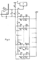
- Figur 3 zeigt eine detaillierte Schaltungsausführung der Erfindung.
- In Figur 1 liegt am Ausgang einer mit IC angedeuteten integrierten Schaltung in PLL-Technik ein Operationsverstärker OP, an dessen Ausgang die Abstimmspannung VT abnehmbar ist, die einem Tuner T zugeführt wird. Vom Ausgang des Operationsverstärkers OP ist eine Gegenkopplung, bestehend aus dem Widerstand R 0, C 0, C 1 auf den invertierenden Eingang des Operationsverstärkers OP eingeführt. Diese Anordnung stellt das Loop-Tiefpassfilter dar, welchem die Abstimmspannung entommen wird. Über den Widerstand RV liegt der Ausgang an einer stabilisierten Spannung von z. B. 33 V. Parallel zum Widerstand R 0 ist erfindungsgemäß eine Widerstandkette R 1 - R n geschaltet, deren Verbindungspunkte 1 - n über Schaltstrecken S 1 - S n mit dem Widerstand R 0 verbindbar sind. Die Schaltstrecken werden von einer Anordnung A in Abhängigkeit von der Abstimmspannung VT betätigt.
- In Abhängigkeit von der Abstimmspannung, d. h. in Abhängigkeit von der eingestellten Frequenz wird die Bandbreite des Filters verändert. Bei tiefen Frequenzen, bei denen die Abstimmspannung sehr klein ist, ist der Kurvenverlauf der C/U-Charakteristik steiler als bei höheren Abstimmspannungen. Je größer die Steilheit, desto mehr können sich Störgrößen auf die mit Hilfe einer Phase-locked-loop-Schaltung erzeugten Abstimmspannung unangenehm bemerkbar machen. Das Filter in der Regelschleife muß also verschieden schnell reagieren. Der Erfindung liegt also die Erkenntnis zugrunde, daß das Tiefpaßverhalten der Filteranordnung geändert werden muß, um stabile Verhältnisse zu erhalten. Der Verlauf der Abstimmspannung wird hierbei nicht beeinflußt.
- Die Abstimmspannung wird hierbei dazu verwendet, um als Kriterium für eine entsprechende Umschaltung des Tiefpaßfilters zu dienen.
- In Figur 2 ist die Abhängigkeit der Kapazitätsdioden von der angelegten Abstimmspannung VT aufgezeichnet. Man erkennt den zunächst sehr steilen Verlauf bei niedrigen Abstimmspannungen, der zu höheren Werten immer flacher wird. Darunter ist in einer Tabelle für die verschiedenen n Abstimmspannungsbereiche die Schalterstellung aufgezeichnet. Die jeweils geschlossenen Schalter sind mit einem X versehen. Die Zahl n richtet sich nach der Referenzfrequenz der PLL-Schaltung und der effektiven Abstimmsteilheit der Diodenkennlinie.
- In Figur 3 wird nachfolgend eine detaillierte Schaltungsanordnung beschrieben. Dabei werden gleiche Bezugszeichen der Figur 1 verwendet. Die Schaltstrecken werden durch Dioden D 11 - D n1 sowie D 12 - D n2 dargestellt, die in Abhängigkeit von der Abstimmspannung VT nacheinander durchgeschaltet werden, sobald die an den Kathoden der Dioden liegende Spannungen den durch die Spannungsteiler R 11, R 12 - R n1, R n2 gebildeten Vorspannungen U 1 - U n unterschritten werden.
- Die Wirkungsweise der Schaltung wird nachstehend an der ersten Schaltstrecke erläutert.
- Am Ausgang einer mit IC angedeuteten integrierten Schaltung in PLL-Technik liegt ein Operationsverstärker OP, an dessen Ausgang die Abstimmspannung VT abnehmbar ist, die einem Tuner T zugeführt wird. Vom Ausgang des Operationsverstärkers OP ist eine Gegenkopplung, bestehend aus dem Widerstand Ro, Co, C, auf den invertierenden Eingang des Operationsverstärkers OP eingefügt. Über den Widerstand Rv liegt der Ausgang an einer stabilisierten Spannung von z. B. +33 V. Parallel zum Widerstand RO ist an die Abstimmspannung VT ein Widerstand R1 über die Reihenschaltung zweier Dioden D11 und D12 parallel geschaltet. Die Dioden D11 und D12 sind mit ihren Anoden verbunden, welche an einen aus den Widerstand R11 und R12 gebildeten Spannungsteiler geschaltet sind der zwischen die Spannungsquelle +33 V und Bezugspotential geschaltet ist. Die sich bildende Vorspannung U1 für die Dioden D11 und D12 ist derart gewählt , daß sie im unteren Abstimmspannungsbereich, d. h. bei steilem Verlauf der Kapazitätsdiodencharakteristik, leitend sind. Bei einem Abstimmspannungswert VT unterhalb dieser Vorspannung U1 ist demnach der Widerstand R1 dem Widerstand RO parallel geschaltet. Durch dieses Parallelschalten des Widerstandes R1 wird die Rückkopplungsimpedanz des Operationsverstärkers OP verringert, wodurch in dem Teil des Abstimmspannungsbereichs mit steilem Verlauf und damit großer Frequenzänderung bei gleichen Abstimmspannungsschritten die Rückkopplung erhöht wird. Hierdurch wird die PLL-Schleife im unteren Abstimmspannungsbereich, in welchem kleine Spannungsänderungen große Frequenzänderungen zur Folge haben, stabilisiert. Durch stärkere Gegenkopplung wird einer Instabilität der Regelung des PLL-Systems entgegengewirkt. Die Erzeugung der Vorspannung U1 für die Dioden D11 und D12 werden von der gleichen stabilisierten Spannung +33 V abgeleitet, von der auch die Abstimmspannung VT abhängt. Dadurch ist die Umschaltung der Gegenkopplung und damit der Zeitkonstanten des Tiefpasses nur von der Abstimmspannung VT abhängig und andere Spannungsschwankungen haben keinen Einfluß.
Claims (3)
Applications Claiming Priority (2)
| Application Number | Priority Date | Filing Date | Title |
|---|---|---|---|
| DE3215747 | 1982-04-28 | ||
| DE3215747A DE3215747C2 (de) | 1982-04-28 | 1982-04-28 | Schaltungsanordnung zum Abstimmen von Hochfrequenzempfängern mit Hilfe einer Phase-Locked-Loop-Schaltung |
Publications (3)
| Publication Number | Publication Date |
|---|---|
| EP0092657A2 EP0092657A2 (de) | 1983-11-02 |
| EP0092657A3 EP0092657A3 (en) | 1985-07-03 |
| EP0092657B1 true EP0092657B1 (de) | 1988-06-29 |
Family
ID=6162118
Family Applications (1)
| Application Number | Title | Priority Date | Filing Date |
|---|---|---|---|
| EP83101803A Expired EP0092657B1 (de) | 1982-04-28 | 1983-02-24 | Schaltungsanordnung zum Abstimmen von Hochfrequenzempfängern mit einer PLL-Schaltung |
Country Status (4)
| Country | Link |
|---|---|
| EP (1) | EP0092657B1 (de) |
| DE (1) | DE3215747C2 (de) |
| ES (1) | ES521380A0 (de) |
| FI (1) | FI79429C (de) |
Families Citing this family (2)
| Publication number | Priority date | Publication date | Assignee | Title |
|---|---|---|---|---|
| US4476583A (en) * | 1983-02-28 | 1984-10-09 | Rca Corporation | Electronic tracking for tuners |
| FR2624323B1 (fr) * | 1987-12-03 | 1994-03-25 | Institut Francais Petrole | Dispositif pour asservir un signal, en frequence et en phase, a celle d'un signal impose |
Citations (1)
| Publication number | Priority date | Publication date | Assignee | Title |
|---|---|---|---|---|
| DE2718472A1 (de) * | 1977-04-26 | 1978-11-02 | Licentia Gmbh | Abstimmschaltung fuer einen hochfrequenz-ueberlagerungsempfaenger mit gleichspannungsgesteuerter abstimmung |
Family Cites Families (3)
| Publication number | Priority date | Publication date | Assignee | Title |
|---|---|---|---|---|
| US3729688A (en) * | 1971-12-15 | 1973-04-24 | Motorola Inc | Oscillator with switchable filter control voltage input for rapidly switching to discrete frequency outputs |
| GB1444860A (en) * | 1974-12-12 | 1976-08-04 | Mullard Ltd | Frequency synthesiser |
| JPS5683135A (en) * | 1979-12-10 | 1981-07-07 | Sony Corp | Pll circuit |
-
1982
- 1982-04-28 DE DE3215747A patent/DE3215747C2/de not_active Expired
-
1983
- 1983-02-24 EP EP83101803A patent/EP0092657B1/de not_active Expired
- 1983-04-11 ES ES521380A patent/ES521380A0/es active Granted
- 1983-04-12 FI FI831213A patent/FI79429C/fi not_active IP Right Cessation
Patent Citations (1)
| Publication number | Priority date | Publication date | Assignee | Title |
|---|---|---|---|---|
| DE2718472A1 (de) * | 1977-04-26 | 1978-11-02 | Licentia Gmbh | Abstimmschaltung fuer einen hochfrequenz-ueberlagerungsempfaenger mit gleichspannungsgesteuerter abstimmung |
Also Published As
| Publication number | Publication date |
|---|---|
| DE3215747C2 (de) | 1986-04-30 |
| FI831213A0 (fi) | 1983-04-12 |
| FI79429C (fi) | 1989-12-11 |
| DE3215747A1 (de) | 1983-11-10 |
| EP0092657A3 (en) | 1985-07-03 |
| FI831213L (fi) | 1983-10-29 |
| FI79429B (fi) | 1989-08-31 |
| EP0092657A2 (de) | 1983-11-02 |
| ES8402482A1 (es) | 1984-01-16 |
| ES521380A0 (es) | 1984-01-16 |
Similar Documents
| Publication | Publication Date | Title |
|---|---|---|
| DE9216205U1 (de) | Kontinuierliche Filterabstimmung mit einer verrasteten Verzögerungsschleife in Massenspeichersystemen oder ähnlichen Systemen | |
| EP1171981A1 (de) | Digitales gmsk-filter | |
| DE19529179C2 (de) | Integrierbare Taktgewinnungsschaltung | |
| DE2836288C2 (de) | Kombi-Tuner | |
| DE112012005546T5 (de) | CR-Schwingkreis | |
| DE19621228A1 (de) | Digital einstellbarer Quarzoszillator mit monolithisch integrierter Oszillatorschaltung | |
| DE68928459T2 (de) | Einen Synthesierer verwendender Frequenzmodulator | |
| EP0166749B1 (de) | Phasenregelkreis | |
| DE3046540A1 (de) | Phasenregelkreis | |
| EP0227156B1 (de) | Regelschaltung zum Abgleich einer Laufzeitleitung | |
| DE3113800A1 (de) | Frequenzmodulator | |
| EP0615343A1 (de) | Schaltungsanordnung zur Erzeugung einer Abstimmspannung | |
| DE4220228A1 (de) | Schaltungsanordnung zur Unterdrückung schmalbandiger Störsignale | |
| EP0092657A2 (de) | Schaltungsanordnung zum Abstimmen von Hochfrequenzempfängern mit einer PLL-Schaltung | |
| DE4220296A1 (de) | Schaltungsanordnung zur Unterdrückung schmalbandiger Störsignale | |
| DE2945546A1 (de) | Schaltungsanordnung fuer abstimmbare hf-kreise | |
| DE3342334C2 (de) | ||
| DE3218363C2 (de) | ||
| EP0170793B1 (de) | Durch binäre Datensignale modulierbarer Hochfrequenzsender | |
| DE10162912A1 (de) | Quarzoszillatorschaltung | |
| DE2718472A1 (de) | Abstimmschaltung fuer einen hochfrequenz-ueberlagerungsempfaenger mit gleichspannungsgesteuerter abstimmung | |
| DE3324919C2 (de) | ||
| DE10312436A1 (de) | Kombinatorisch geschaltete Steuerspannung für Multiband-VCOs | |
| DE2912710C3 (de) | Abstimmschaltung für einen Empfänger, deren Abstimmlage von dem Stand eines Zählers bestimmt wird | |
| DE2735031C3 (de) | Phasenregelkreis |
Legal Events
| Date | Code | Title | Description |
|---|---|---|---|
| PUAI | Public reference made under article 153(3) epc to a published international application that has entered the european phase |
Free format text: ORIGINAL CODE: 0009012 |
|
| AK | Designated contracting states |
Designated state(s): BE CH FR GB IT LI NL SE |
|
| PUAL | Search report despatched |
Free format text: ORIGINAL CODE: 0009013 |
|
| AK | Designated contracting states |
Designated state(s): BE CH FR GB IT LI NL SE |
|
| 17P | Request for examination filed |
Effective date: 19851210 |
|
| 17Q | First examination report despatched |
Effective date: 19870203 |
|
| ITF | It: translation for a ep patent filed | ||
| GRAA | (expected) grant |
Free format text: ORIGINAL CODE: 0009210 |
|
| AK | Designated contracting states |
Kind code of ref document: B1 Designated state(s): BE CH FR GB IT LI NL SE |
|
| GBT | Gb: translation of ep patent filed (gb section 77(6)(a)/1977) | ||
| ET | Fr: translation filed | ||
| PLBE | No opposition filed within time limit |
Free format text: ORIGINAL CODE: 0009261 |
|
| STAA | Information on the status of an ep patent application or granted ep patent |
Free format text: STATUS: NO OPPOSITION FILED WITHIN TIME LIMIT |
|
| 26N | No opposition filed | ||
| ITTA | It: last paid annual fee | ||
| EAL | Se: european patent in force in sweden |
Ref document number: 83101803.1 |
|
| PGFP | Annual fee paid to national office [announced via postgrant information from national office to epo] |
Ref country code: GB Payment date: 19960213 Year of fee payment: 14 |
|
| PGFP | Annual fee paid to national office [announced via postgrant information from national office to epo] |
Ref country code: FR Payment date: 19960216 Year of fee payment: 14 |
|
| PGFP | Annual fee paid to national office [announced via postgrant information from national office to epo] |
Ref country code: NL Payment date: 19960220 Year of fee payment: 14 |
|
| PGFP | Annual fee paid to national office [announced via postgrant information from national office to epo] |
Ref country code: SE Payment date: 19960221 Year of fee payment: 14 Ref country code: BE Payment date: 19960221 Year of fee payment: 14 |
|
| PGFP | Annual fee paid to national office [announced via postgrant information from national office to epo] |
Ref country code: CH Payment date: 19960227 Year of fee payment: 14 |
|
| PG25 | Lapsed in a contracting state [announced via postgrant information from national office to epo] |
Ref country code: GB Effective date: 19970224 |
|
| PG25 | Lapsed in a contracting state [announced via postgrant information from national office to epo] |
Ref country code: SE Effective date: 19970225 |
|
| PG25 | Lapsed in a contracting state [announced via postgrant information from national office to epo] |
Ref country code: LI Effective date: 19970228 Ref country code: CH Effective date: 19970228 Ref country code: BE Effective date: 19970228 |
|
| BERE | Be: lapsed |
Owner name: DEUTSCHE THOMSON-BRANDT G.M.B.H. Effective date: 19970228 |
|
| PG25 | Lapsed in a contracting state [announced via postgrant information from national office to epo] |
Ref country code: NL Effective date: 19970901 |
|
| GBPC | Gb: european patent ceased through non-payment of renewal fee |
Effective date: 19970224 |
|
| REG | Reference to a national code |
Ref country code: CH Ref legal event code: PL |
|
| PG25 | Lapsed in a contracting state [announced via postgrant information from national office to epo] |
Ref country code: FR Effective date: 19971030 |
|
| EUG | Se: european patent has lapsed |
Ref document number: 83101803.1 |
|
| NLV4 | Nl: lapsed or anulled due to non-payment of the annual fee |
Effective date: 19970901 |
|
| REG | Reference to a national code |
Ref country code: FR Ref legal event code: ST |