EP0091815A2 - Statische Halbleiterspeicheranordnung - Google Patents
Statische Halbleiterspeicheranordnung Download PDFInfo
- Publication number
- EP0091815A2 EP0091815A2 EP83302037A EP83302037A EP0091815A2 EP 0091815 A2 EP0091815 A2 EP 0091815A2 EP 83302037 A EP83302037 A EP 83302037A EP 83302037 A EP83302037 A EP 83302037A EP 0091815 A2 EP0091815 A2 EP 0091815A2
- Authority
- EP
- European Patent Office
- Prior art keywords
- current
- holding
- memory
- source
- circuit
- Prior art date
- Legal status (The legal status is an assumption and is not a legal conclusion. Google has not performed a legal analysis and makes no representation as to the accuracy of the status listed.)
- Granted
Links
Images
Classifications
-
- G—PHYSICS
- G11—INFORMATION STORAGE
- G11C—STATIC STORES
- G11C5/00—Details of stores covered by group G11C11/00
- G11C5/005—Circuit means for protection against loss of information of semiconductor storage devices
-
- G—PHYSICS
- G11—INFORMATION STORAGE
- G11C—STATIC STORES
- G11C11/00—Digital stores characterised by the use of particular electric or magnetic storage elements; Storage elements therefor
- G11C11/21—Digital stores characterised by the use of particular electric or magnetic storage elements; Storage elements therefor using electric elements
- G11C11/34—Digital stores characterised by the use of particular electric or magnetic storage elements; Storage elements therefor using electric elements using semiconductor devices
- G11C11/40—Digital stores characterised by the use of particular electric or magnetic storage elements; Storage elements therefor using electric elements using semiconductor devices using transistors
- G11C11/41—Digital stores characterised by the use of particular electric or magnetic storage elements; Storage elements therefor using electric elements using semiconductor devices using transistors forming static cells with positive feedback, i.e. cells not needing refreshing or charge regeneration, e.g. bistable multivibrator or Schmitt trigger
- G11C11/413—Auxiliary circuits, e.g. for addressing, decoding, driving, writing, sensing, timing or power reduction
- G11C11/414—Auxiliary circuits, e.g. for addressing, decoding, driving, writing, sensing, timing or power reduction for memory cells of the bipolar type
- G11C11/416—Read-write [R-W] circuits
Definitions
- the present invention relates to a static-type semiconductor memory device.
- a static-type semiconductor memory device comprises a memory cell array consisting of a plurality of memory cells, a peripheral circuit for this memory cell array, and a holding-current supplying circuit.
- Each static-type memory cell comprises cross--coupled transistors which constitute a flip-flop.
- the data storing capacity of this memory cell is expressed by 1 ⁇ 2CV, where C is the amount of the stored charges, and V is the base-base voltage when the above-mentioned transistors are bipolar transistors, or the gate-gate voltage when the above-mentioned transistors are metal-insulator semiconductor (MIS) transistors.
- MIS metal-insulator semiconductor
- IL is desirable to provide a static-type semiconductor memory device in which the danger of destruction of the stored data by alpha particles or power supply noise is reduced.
- An embodiment of the present invention can provide a static-type semiconductor memory device in which the C and V in each memory cell in unselected memory IC's are made greater than those in each memory cell in selected memory IC's.
- An embodiment of the present invention can provide a static-type semiconductor memory device in which the holding current flowing through memory cells in selected-state memory IC's is greater than the holding current flowing through memory cells in unselected-state memory IC's.
- Such an embodiment of the present invention can comprise a static-type semiconductor memory device comprising a plurality of memory blocks arranged in a row direction and in a column direction to form a matrix. Any one row of the memory blocks is operatively selected to carry out a reading or writing operation in the selected memory blocks.
- Each of the memory blocks comprises a memory cell array, consisting of memory cells, and a peripheral circuit, associated with the memory cell array.
- the peripheral circuit comprises a holding-current supplying circuit for supplying to the memory blocks a current for holding data stored in the memory cells, a first current--source circuit for supplying currents through bit lines to the memory cells, a sense amplifier circuit for detecting potential differences between the bit lines, and a second current-source circuit for supplying currents to the sense amplifier circuit.
- Each of the memory blocks further comprises a holding-current controlling circuit for controlling the holding-current supplying circuit such that the holding current supplied to an unselected-state memory block is greater than-the holding current supplied to a selected-state memory block and that the current supplied to the first current-source circuit, the sense amplifier, and the second current-source circuit, associated with an unselected-state memory block is smaller than the current supplied to the first current--source circuit, the sense amplifier, and the second current-source circuit, associated with a selected-state memory block.
- the holding-current controlling circuit comprises a differential amplifier for determining whether the memory block is selected or not.
- the differential amplifier operatively outputs a holding-current determining signal.
- the holding-current determining signal has a first potential when the memory block is selected and has a second potential when the memory block is unselected.
- the holding-current determining signals is operatively applied to the holding-current supplying circuit so as to activate the holding-current supplying circuit in response to only the first potential.
- the differential amplifier operatively outputs a current--source current determining signal having the first potential or the second potential when the holding--current determining signal has the second potential or the first potential, respectively.
- the current-source current determining signal is applied to the first current source and the second current source so as to activate the current sources in response to the potential of the current-source current determining signal.
- each of the memory cells is connected between a word line and a hold line.
- the word line and the hold line are extended in the row direction.
- the holding current is conducted from the word line through the memory cell to the hold line.
- Each of the memory cells is connected between a pair of bit lines extending in the column direction.
- the holding-current supplying circuit comprises a plurality of first NPN transistors each having a base adapted to receive the holding--current determining signal from the d fferential amplifier, a collector connected to the hold line, and an emitter connected to a first power supply.
- the first current source and the second current source comprise second NPN transistors each having a base adapted to receive the current-source current determining signal.
- the differential amplifier comprises: a third NPN transistor, having a base adapted to receive a reference signal, a collector connected through a resistor to a second power supply, and an emitter connected to current source; and a fourth NPN transistor, having a base adapted to receive a block selecting signal, a collector connected through a resistor to the second power supply, and an emitter connected to the current source.
- the collector of the third NPN transistor is adapted to provide the holding-current determining signal.
- the collector of the fourth NPN transistor is adapted to provide the current-source current determining signal.
- Each of the memory blocks may comprise one memory chip.
- a predetermined number of the memory blocks may constitute one memory chip.
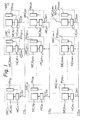
- FIG. 1 is a general block diagram of an embodiment of the present invention.
- MIC 11 through MIC mn are memory IC chips
- MCA 11 through MCA mn are memory cell arrays
- PH 11 through PH mn are peripheral circuits of the memory cell arrays
- HC 11 through HC mn are holding-current controlling circuits
- CS 11 through CS mn are chip-selecting terminals
- CS 1 through CS are chip-selecting signals.
- Each static-type semiconductor memory IC chip comprises a memory cell array, a peripheral circuit, and a holding-current controlling circuit for controlling the holding current supplied to the memory cell array and the current supplied to the peripheral circuit.
- the ratio between the holding current supplied to the memory cells in this chip and the current supplied to the peripheral circuit in this chip is the same as the ratio in conventional devices.
- the memory IC chip is in an unselected state, i.e., when the chip-selecting signal is at a high level, the holding current supplied to the memory cells in this chip is increased, and the current supplied to the peripheral circuit in this chip is decreased.
- the total power consumption in all of the memory IC chips is thus either constant or decreased. Thus, almost no data stored in the unselected-state memory cells are destroyed because of the increased holding currents.
- the current flowing through the peripheral circuits PH 21 , ---, PH 2n ' ---, and PH mn in and after the second row becomes smaller than the current flowing through the selected-state peripheral circuits, as described in detail later. Since no writing or reading operation is carried out in the unselected-state memory IC chips, the operating speed is not reduced even when the holding current supplied to the unselected memory IC chips is increased. Also, since the peripheral circuit does not operate in the unselected state, the current supplied to the peripheral circuit in the unselected memory IC chip can be decreased without any trouble.
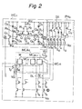
- FIG. 2 is a circuit diagram of one of the memory IC chips MIC 11 in the block diagram of Fig. 1.
- the memory IC chip MIC 11 includes the memory cell array MCA 11 , its peripheral circuit PH 11 , and the holding--current controlling circuit HC 11 .
- the memory cell array MCA 11 and the peripheral circuit PH 11 have well known constructions.
- the memory cell array MCA 11 has bipolar memory cells MC 11 ' ---, MC ln , --- arranged in a matrix.
- the peripheral circuit PH 11 includes a word-line driving transistor T 1 and a holding-current supplying transistor T 2 for each row of the memory cell array, bit-line level detecting transistors T 3 and T 4 , transistors T 5 and T 6 for supplying currents to the bit lines BL and BL, and a well-known sense amplifier SA, for each column of the memory cell array.
- the detected levels of the bit lines BL and BL are amplified to obtain the read-out data at an output terminal D 0 .
- Transistors T 7 through T 12 in the peripheral circuit PH 11 are transistors for a current source for the sense amplifier.
- the other sense amplifiers for the memory cells MC 11 through MC 1n-1 and their peripheral circuits are eliminated in the drawing.
- the holding-current controlling circuit HC 11 in the illustrated embodiment of the invention comprises a pair of NPN transistors Q 1 and Q 2 .
- a reference voltage Ref is operatively applied to the base of the Q 1 .
- a chip-selecting signal CS 1 is operatively applied.
- the emitters of the transistors Q 1 and Q 2 are commonly connected to a current source I 0 .
- the collectors of the transistors Q 1 and Q 2 are respectively connected via resistors R 1 and R 2 to one end of the resistor R 3 , the other end of the resistor R 3 being connected to a power supply line V CC .
- the collectors of the transistors Q 1 and Q 2 are also connected to the bases of NPN transistors Q 3 and Q 4 , respectively.
- the collectors of the transistors Q 3 and Q 4 are connected to the power supply line V CC .
- the emitters of the transistors Q 3 and Q 4 are respectively connected via resistors R 4 and R 5 to the collectors of NPN transistors Q 5 and Q 6 .
- the emitters of the transistors Q 5 and Q 6 are connected to the ground-power supply line V EE .
- the bases of the transistors Q 5 and Q 6 are respectively clamped by diodes D 1 and D 2 .
- the anodes of the diodes D 1 and D 2 are respectively connected to the bases of the transistors Q 5 and Q 6 , and the cathodes of the diodes D 1 and D 2 are connected to the ground-power supply line V EE .
- the anodes of the diodes D 1 and D 2 are respectively connected via resistors R 6 and R 7 to the cathodes of diodes D 3 and D 4 .
- the anodes of the diodes D 3 and D 4 are connected to the power supply line V CC .
- the collectors of the transistors Q 5 and Q 6 are also connected to the bases of transistors Q 7 and Q 8 , respectively.
- the collectors of the transistors Q 7 and Q 8 are connected to the power supply line V CC , and the emitters of the transistors Q 7 and Q 8 are connected via resistors R 8 and R 9 , respectively, to the ground-power supply line V EE .
- the emitter A of the transistor Q 7 is also connected to the base of the holding-current supplying transistor T 2 in this memory cell array MCA 11 .
- the emitter B of the transistor Q 8 is also connected to the bases of the transistors T 7 through T 12 and to the bases of the current-source transistors such as the transistors T 5 and T 6 for the bit lines.
- the memory IC chips MIC 11 , ---, and MIC ln in the first row as shown in Fig. 1 are in the unselected state.
- the transistor Q 1 is off, and the transistor Q 2 is on.
- the base level of the transistor Q 3 is at the H level
- the base level of the transistor Q 4 is at the L level.
- the collector level of the transistor Q S or the base level of the transistor Q 7 becomes the H level
- the collector level of the transistor Q 6 or the base level of the transistor Q 8 becomes the L level.
- the potential at the emitter A of the transistor Q 7 becomes the H level
- the potential at the emitter B of the transistor Q 8 becomes the L level. Accordingly, to the base of the holding-current supplying transistor T 2 in the memory cell array MCA 11 , the H level voltage is applied to turn on the transistor T 2 so that a large holding current I H flows from the word line W through the memory cells MC 11 through MC ln and through the transistor T 2 to the ground-power supply line V EE .
- the L level potential is applied to the bases of the current source transistors T 7 through T12 and to the bases of the bit-line current source transistors T 5 , T 6 , ---, these transistors T 5 through T12 are turned off so that the current flowing through the peripheral circuit PH 11 is decreased.
- the holding current for the unselected-state memory cells and the current for their peripheral circuit are set to the appropriate values so that the increase in the power consumption due to the increase of the holding current is compensated with or decreased by the decrease in the power consumption due to the decreased current flowing through the peripheral circuit, the total power consumption in the memory IC chip MIC 11 is constant regardless of its selected state or unselected state, or may be decreased in comparison with its selected state.
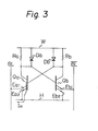
- Figure 3 is an equivalent circuit diagram of an example of a well-known bipolar memory cell.
- the memory cell MC comprises, as is well known, a pair of multi- emitter NPN transistors Q a and Q b , a load resistor R a and a clamping diode D a connected in parallel between the collector of the transistor Q a and the word line W + , and a load resistor R b and a clamping diode D b connected in parallel between the collector of the transistor Q b and the word line W + .
- the first emitters E al and E bl of the transistors Q a and Q b are connected to the bit lines BL and BL, respectively. These emitters E al and E bl are referred to as detecting emitters.
- the second emitters E a2 and E b2 are connected to a hold line H. These emitters E a2 and E b2 are referred to as holding emitters. So long as the voltage between both ends of the resistor R a or R b is smaller than the clamping voltage of the diode D a or D b , a current flows through the resistor R or R b .
- the greater the holding current I H the greater the potential difference V between the bases. Since the data holding capacity can be expressed by 1 ⁇ 2CV, as described before, the data holding capacity of each memory cell in the unselected memory IC chips is increased by increasing the holding current I H .
- a PNPN-type memory cell is also known.
- the PNPN--type memory cell uses diodes as the loads. Each of these diodes is formed between the emitter and the base of a PNP transistor.
- the voltage drop between the ends of the load is not increased even when the holding current is increased. Accordingly, the potential difference between the bases of the transistors which constitute the flip-flop is not increased.
- the holding current I H is increased, the depletion layer of the load PNP transistor is narrowed due to the increase in the forward-direction bias current. Therefore, the capacity C is increased, and, thus, the data holding capacity 2 V is also increased.
- the above explanation has been made in reference to examples using bipolar transistors in memory cells. However, it will be apparent to those skilled in the art that the present invention is also applicable to a static-type semiconductor memory device using MIS transistors. Also, the above explanation described the holding current being increased when the memory IC is unselected. Alternatively, the memory cell array in the memory IC may be separated into several blocks, and the holding current in the unselected-block memory cells may be increased and the supplying current to its peripheral circuit may be decreased.
Landscapes
- Engineering & Computer Science (AREA)
- Microelectronics & Electronic Packaging (AREA)
- Computer Hardware Design (AREA)
- Static Random-Access Memory (AREA)
Applications Claiming Priority (2)
| Application Number | Priority Date | Filing Date | Title |
|---|---|---|---|
| JP57059763A JPS58177591A (ja) | 1982-04-12 | 1982-04-12 | スタテイツク型半導体記憶装置 |
| JP59763/82 | 1982-04-12 |
Publications (3)
| Publication Number | Publication Date |
|---|---|
| EP0091815A2 true EP0091815A2 (de) | 1983-10-19 |
| EP0091815A3 EP0091815A3 (en) | 1986-02-05 |
| EP0091815B1 EP0091815B1 (de) | 1989-01-11 |
Family
ID=13122630
Family Applications (1)
| Application Number | Title | Priority Date | Filing Date |
|---|---|---|---|
| EP83302037A Expired EP0091815B1 (de) | 1982-04-12 | 1983-04-12 | Statische Halbleiterspeicheranordnung |
Country Status (4)
| Country | Link |
|---|---|
| US (1) | US4604729A (de) |
| EP (1) | EP0091815B1 (de) |
| JP (1) | JPS58177591A (de) |
| DE (1) | DE3378937D1 (de) |
Families Citing this family (2)
| Publication number | Priority date | Publication date | Assignee | Title |
|---|---|---|---|---|
| JPS59167895A (ja) * | 1983-03-14 | 1984-09-21 | Nec Corp | 半導体メモリ回路 |
| US4796227A (en) * | 1987-03-17 | 1989-01-03 | Schlumberger Systems And Services, Inc. | Computer memory system |
Family Cites Families (4)
| Publication number | Priority date | Publication date | Assignee | Title |
|---|---|---|---|---|
| US4198698A (en) * | 1978-12-06 | 1980-04-15 | Fairchild Camera And Instrument Corporation | Chip select power-down control circuitry |
| JPS5831673B2 (ja) * | 1979-08-22 | 1983-07-07 | 富士通株式会社 | 半導体記憶装置 |
| JPS5847793B2 (ja) * | 1979-11-12 | 1983-10-25 | 富士通株式会社 | 半導体記憶装置 |
| JPS5712481A (en) * | 1980-06-26 | 1982-01-22 | Mitsubishi Electric Corp | Semiconductor memory device |
-
1982
- 1982-04-12 JP JP57059763A patent/JPS58177591A/ja active Granted
-
1983
- 1983-04-05 US US06/482,301 patent/US4604729A/en not_active Expired - Fee Related
- 1983-04-12 DE DE8383302037T patent/DE3378937D1/de not_active Expired
- 1983-04-12 EP EP83302037A patent/EP0091815B1/de not_active Expired
Also Published As
| Publication number | Publication date |
|---|---|
| EP0091815A3 (en) | 1986-02-05 |
| US4604729A (en) | 1986-08-05 |
| JPH043036B2 (de) | 1992-01-21 |
| JPS58177591A (ja) | 1983-10-18 |
| DE3378937D1 (en) | 1989-02-16 |
| EP0091815B1 (de) | 1989-01-11 |
Similar Documents
| Publication | Publication Date | Title |
|---|---|---|
| US4078261A (en) | Sense/write circuits for bipolar random access memory | |
| US4745582A (en) | Bipolar-transistor type random access memory device having redundancy configuration | |
| US4322820A (en) | Semiconductor integrated circuit device | |
| US4348747A (en) | System for driving bipolar ram | |
| US4984207A (en) | Semiconductor memory device | |
| US4295210A (en) | Power supply system for monolithic cells | |
| US4464735A (en) | Semiconductor memory | |
| EP0202892B1 (de) | Halbleiterspeichergerät mit Diodenmatrixdecodierer und Redundanzkonfiguration | |
| EP0503524A2 (de) | Halbleiterspeicheranordnung | |
| EP0117646B1 (de) | Halbleiterspeicheranordnung mit Steuerschaltung zum Lesen-Schreiben | |
| EP0091815A2 (de) | Statische Halbleiterspeicheranordnung | |
| US4742488A (en) | Sense amplifier/write circuit for semiconductor memories | |
| EP0130414A2 (de) | Verzeichnisspeicher | |
| US4730275A (en) | Circuit for reducing the row select voltage swing in a memory array | |
| EP0031009A1 (de) | Vielfachzugriff-Speicherzelle und ihre Anwendung in einer Speichermatrix | |
| US4456979A (en) | Static semiconductor memory device | |
| US4922411A (en) | Memory cell circuit with supplemental current | |
| US4592023A (en) | Latch for storing a data bit and a store incorporating said latch | |
| US4697251A (en) | Bipolar RAM cell | |
| KR910002502B1 (ko) | 복수개의 가변 클램프형 메모리 셀을 구비한 메모리 회로 | |
| US4635231A (en) | Semiconductor memory with constant readout capability | |
| US4570238A (en) | Selectable write current source for bipolar rams | |
| JPH0529993B2 (de) | ||
| US4899311A (en) | Clamping sense amplifier for bipolar ram | |
| EP0037734B1 (de) | Halbleiterspeicherbaustein und Speicheranordnung mit solchen Bausteinen |
Legal Events
| Date | Code | Title | Description |
|---|---|---|---|
| PUAI | Public reference made under article 153(3) epc to a published international application that has entered the european phase |
Free format text: ORIGINAL CODE: 0009012 |
|
| AK | Designated contracting states |
Designated state(s): DE FR GB |
|
| PUAL | Search report despatched |
Free format text: ORIGINAL CODE: 0009013 |
|
| AK | Designated contracting states |
Designated state(s): DE FR GB |
|
| 17P | Request for examination filed |
Effective date: 19860326 |
|
| 17Q | First examination report despatched |
Effective date: 19870326 |
|
| GRAA | (expected) grant |
Free format text: ORIGINAL CODE: 0009210 |
|
| AK | Designated contracting states |
Kind code of ref document: B1 Designated state(s): DE FR GB |
|
| REF | Corresponds to: |
Ref document number: 3378937 Country of ref document: DE Date of ref document: 19890216 |
|
| ET | Fr: translation filed | ||
| PLBE | No opposition filed within time limit |
Free format text: ORIGINAL CODE: 0009261 |
|
| STAA | Information on the status of an ep patent application or granted ep patent |
Free format text: STATUS: NO OPPOSITION FILED WITHIN TIME LIMIT |
|
| 26N | No opposition filed | ||
| PGFP | Annual fee paid to national office [announced via postgrant information from national office to epo] |
Ref country code: GB Payment date: 19920204 Year of fee payment: 10 |
|
| PGFP | Annual fee paid to national office [announced via postgrant information from national office to epo] |
Ref country code: FR Payment date: 19920429 Year of fee payment: 10 |
|
| PGFP | Annual fee paid to national office [announced via postgrant information from national office to epo] |
Ref country code: DE Payment date: 19920623 Year of fee payment: 10 |
|
| PG25 | Lapsed in a contracting state [announced via postgrant information from national office to epo] |
Ref country code: GB Effective date: 19930412 |
|
| GBPC | Gb: european patent ceased through non-payment of renewal fee |
Effective date: 19930412 |
|
| PG25 | Lapsed in a contracting state [announced via postgrant information from national office to epo] |
Ref country code: FR Effective date: 19931229 |
|
| PG25 | Lapsed in a contracting state [announced via postgrant information from national office to epo] |
Ref country code: DE Effective date: 19940101 |
|
| REG | Reference to a national code |
Ref country code: FR Ref legal event code: ST |