EP0090662A2 - Boosting circuit - Google Patents
Boosting circuit Download PDFInfo
- Publication number
- EP0090662A2 EP0090662A2 EP83301820A EP83301820A EP0090662A2 EP 0090662 A2 EP0090662 A2 EP 0090662A2 EP 83301820 A EP83301820 A EP 83301820A EP 83301820 A EP83301820 A EP 83301820A EP 0090662 A2 EP0090662 A2 EP 0090662A2
- Authority
- EP
- European Patent Office
- Prior art keywords
- circuit
- mos transistor
- terminals
- level
- capacitor
- Prior art date
- Legal status (The legal status is an assumption and is not a legal conclusion. Google has not performed a legal analysis and makes no representation as to the accuracy of the status listed.)
- Granted
Links
- 239000003990 capacitor Substances 0.000 claims abstract description 57
- 238000010586 diagram Methods 0.000 description 6
- 230000015572 biosynthetic process Effects 0.000 description 3
- 238000010276 construction Methods 0.000 description 3
- 238000009413 insulation Methods 0.000 description 3
- 230000000694 effects Effects 0.000 description 2
- 239000004065 semiconductor Substances 0.000 description 2
- 230000007423 decrease Effects 0.000 description 1
- 239000003989 dielectric material Substances 0.000 description 1
- 229910044991 metal oxide Inorganic materials 0.000 description 1
- 150000004706 metal oxides Chemical class 0.000 description 1
- 239000000758 substrate Substances 0.000 description 1
Images


Classifications
-
- H—ELECTRICITY
- H03—ELECTRONIC CIRCUITRY
- H03K—PULSE TECHNIQUE
- H03K17/00—Electronic switching or gating, i.e. not by contact-making and –breaking
- H03K17/51—Electronic switching or gating, i.e. not by contact-making and –breaking characterised by the components used
- H03K17/56—Electronic switching or gating, i.e. not by contact-making and –breaking characterised by the components used by the use, as active elements, of semiconductor devices
- H03K17/687—Electronic switching or gating, i.e. not by contact-making and –breaking characterised by the components used by the use, as active elements, of semiconductor devices the devices being field-effect transistors
- H03K17/693—Switching arrangements with several input- or output-terminals, e.g. multiplexers, distributors
-
- H—ELECTRICITY
- H03—ELECTRONIC CIRCUITRY
- H03K—PULSE TECHNIQUE
- H03K17/00—Electronic switching or gating, i.e. not by contact-making and –breaking
- H03K17/04—Modifications for accelerating switching
- H03K17/041—Modifications for accelerating switching without feedback from the output circuit to the control circuit
- H03K17/0412—Modifications for accelerating switching without feedback from the output circuit to the control circuit by measures taken in the control circuit
- H03K17/04123—Modifications for accelerating switching without feedback from the output circuit to the control circuit by measures taken in the control circuit in field-effect transistor switches
-
- H—ELECTRICITY
- H03—ELECTRONIC CIRCUITRY
- H03K—PULSE TECHNIQUE
- H03K17/00—Electronic switching or gating, i.e. not by contact-making and –breaking
- H03K17/06—Modifications for ensuring a fully conducting state
-
- H—ELECTRICITY
- H03—ELECTRONIC CIRCUITRY
- H03K—PULSE TECHNIQUE
- H03K19/00—Logic circuits, i.e. having at least two inputs acting on one output; Inverting circuits
- H03K19/02—Logic circuits, i.e. having at least two inputs acting on one output; Inverting circuits using specified components
- H03K19/08—Logic circuits, i.e. having at least two inputs acting on one output; Inverting circuits using specified components using semiconductor devices
- H03K19/094—Logic circuits, i.e. having at least two inputs acting on one output; Inverting circuits using specified components using semiconductor devices using field-effect transistors
- H03K19/096—Synchronous circuits, i.e. using clock signals
Definitions
- the present invention relates to a boosting circuit, more particularly to a boosting circuit used as a multichannel input circuit.
- IC semiconductor integrated circuits
- TTL transistor--transistor logic
- MOS transistors comprising the IC each have their own threshold voltage levels, i.e., V th . Therefore, even if an external signal of 5 V is applied to an input of the IC, the inputted singal is changed to one having a reduced voltage of, for example, (5 - V th ) V, when introduced inside the IC.
- the above-mentioned prior art boosting circuit suffers from the problem that the required formation of many channels, as the multichannel input circuit in the IC make realization of a highly dense IC package impossible. Also, a complicated circuit construction is needed for forming the boosting circuit.
- variable capacitors for each channel wherein each capacitance is controllable according to the voltage level applied thereto.
- Figure 1 is a circuit diagram of an example of an input circuit to which the present invention is adapted.
- reference numeral 11 represents a boosting circuit, to which the present invention is concerned.
- the boosting circuit 11 cooperates with an input circuit 12.
- the present invention is particularly advantageous when the input circuit 12 has a multichannel construction, as represented by numerals 13-1 through 13-n (n is positive integer other than 1).
- Each channel (13-1 through 13-n) of the multichannel is fabricated by using a transfer gate made of a MOS transistor, as represented by numerals 14-1 through 14-n.
- a transfer gate made of a MOS transistor, as represented by numerals 14-1 through 14-n.
- the circuit 15 can be of any type and is not relevant to the present invention. However, if it is an analog/digital converting circuit, error may occur in the converted digital signals, since the input signals S 1 through S n would not maintain their initial levels of voltage at each input stage of the IC. The error is caused since the transfer gates 14-1 through 14-n necessarily have threshold voltage levels V th . Thus, the input signals S 1 through S n , which have, for example, an inherent voltage of 5 V, would be reduced to a voltage of 15 - V th ) V when reaching the input of the circuit 15.
- a voltage exceeding the maximum voltage of 5 V e.g., 7 V, is conventionally applied to each control gate of the transfer gates 14-1 through 14-n. This allows the supply of input signals S1 through S n of a voltage level of 5 V to the circuit 15. Such a voltage increase at the gate is achieved by means of a boosting circuit.
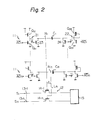
- FIG. 2 is a circuit diagram of an example of the prior art boosting circuit.
- members the same as those of Fig. 1 are represented by the same reference numerals or symbols, (same for later figures).
- Boosting circuits 11 of the same circuit construction are formed for each channel. The following explanation is made taking one of the boosting circuits 11 illustrated at the top of this figure as an example.
- the boosting circuit 11 cooperates with the transfer gate 14-1 forming a part of the channel 13-1.
- a node N 1 in the boosting circuit 11 is connected to the control gate of the transfer gate 14-1 by way of a line L l .
- a node N 1 is also connected to a capacitor C l .
- a first buffer circuit 21 is formed at the side of a first terminal (left side) of the capacitor C 1 .
- a second buffer circuit 22 is formed at the side of a second terminal (right side) of this capacitor C 1 .
- Figure 3 depicts waveforms of signals appearing at major portions in Fig. 2.
- an address signal AD 1 having a waveform shown in row (1) of Fig. 3 is supplied, as an inverted signal AD 1 , so as to selectively activate the boosting circuit 11. Therefore, the signal AD l having an inverted logic level of AD 1 ("H" (high)), i.e., "L” (low), is applied to the first and second buffer circuits 21 and 22.
- Transistors Q 11 and Q 21 are turned off, and, thereby, both the first and second terminals of the capacitor C 1 would increase to the "H" level.
- transistors 23 and 24 are still maintained on by timing pulse ⁇ and ⁇ , respectively. Therefore, the first and second terminals of the capacitor C 1 are still maintained at the "L" level.
- the timing pulse ⁇ of the "H" level is given at the first time t 1 in row (2) of Fig. 3.
- the transistor 23 is turned off since it receives the timing pulse ⁇ having an inverted logic level of ⁇ .
- the first terminal of the capacitor C 1 increases in voltage level toward a level of V shown in row (4) of Fig. 3, which level V is about 5 V.
- the timing pulse ⁇ of the "H” level is given.
- the transistor 22 is also turned off since it receives the timing pulse ⁇ ' having an inverted logic level of ⁇ . Soon after this, the second terminal of the capacitor C1 increases in voltage level toward the "H" level.
- the bootstrap effect starts, so that the first terminal of the capacitor C 1 is increase in voltage level over level V and reaches a level of V' as shown in row (4) of Fig. 3, which level V' is about 7 V.
- the voltage V' is applied via the node N 1 and the line L 1 , to the control gate, as a gate voltage V G , of the transfer gate 14-1. Consequently, a high voltage exceeding 5 V can be given to the control gate, as desired.
- a transistor Q 12 of the first buffer circuit 21 is then in cut-off state due to the high voltage of level V'.
- a transistor Q22 preferably made of a depletion type MOS transistor, functions as a load transistor so as to fully increase the voltage level at the second terminal of the capacitor C1 up to the power source level.
- the second buffer circuit side (right side in this figure) is relatively redundant. This results in an increase of the number of circuit elements concerned. Thus, it is desirable, to realize the same function as that of the groups of second buffer circuits by means of a single second buffer circuit, not for individual channels but common to all channels.
- FIG. 4 is a circuit diagram of a boosting circuit according to a first embodiment of the present invention and an ordinary input circuit cooperating therewith.
- each of boosting circuits 41 is provided with a variable capacitor (instead of the prior art capacitors C 1 through C n in Fig. 2).
- the variable capacitors are preferably made of a MOS transistor capacitor, most preferably, of a depletion-type MOS transistor capacitor.
- the variable capacitors for the channels are illustrated as MOS transistor capacitors 42-1 through 42-n.
- the second buffer circuits 22 for individual channels in Fig. 2 are replaced by a single second buffer circuit 22' common to all channels.
- the feature of the present invention is of the MOS transistor capacitors 42-1 through 42-n, that for the selected one of the channels exhibits the largest capacitance, while the remaining ones for the remaining nonselected channels exhibit the least capacitance.
- the single second buffer circuit 22' always carries one capacitance component only, as load, created by the MOS transistor capacitor for the selected one of the channels. Accordingly, in the present invention, the capacitance load is not extremely large as in the prior art circuit of Fig. 2.
- the MOS transistor capacitor 42-1 is for the selected one of the channels, a so-called channel, i.e., p-channel or n-channel, is formed between a source S and a drain D of the selected MOS transistor capacitor 42-1, which results in increasing the capacitance value thereof.
- a so-called channel i.e., p-channel or n-channel
- the MOS transistor capacitor 42-n such a channel is not formed because these are in cut-off states. This decreases their capacitance values whether the MOS transistor capacitor is cut-off or not is determined in accordance with the relationship in level between a voltage V applied to its gate G and a voltage V SD applied to both its source S and drain D.
- each MOS transistor capacitor is most preferably made of a depletion-type MOS transistor capacitor.
- the reason for this is that each nonselected MOS transistor capacitor is always maintained, under the condition of V G ⁇ V SD , in the cut-off state. If each MOS transistor capacitor is made of an enhancement-type MOS transistor capacitor, the cut-off state cannot always be guaranteed under the same condition as above. Thus, the depletion-type MOS transistor capacitor is preferable in practical use.
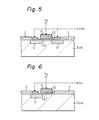
- FIG. 5 is a cross-sectional view of a MOS transistor capacitor shown in Fig. 4.
- reference symbol Sub corresponds to a substrate, I to an insulation layer, G to the gate, S to the source, and D to the drain.
- the voltages V G and V SD are applied in the manner shown in this figure.
- the MOS transistor capacitor functions as a capacitor having a dielectric material made with a gate insulation GI formed just beneath the gate G.
- the aforesaid channel i.e., p-channel or n-channel, is selectively formed just beneath the gate insulation GI, as shown by reference symbol CH.
- the related capacitor exhibits a large capacitance value.
- the capacitance value is variable in accordance with the relationship in level between the voltages V G and VSD.
- This known fact is cleverly utilized, in the present invention in establishing the boosting circuit cooperating with the multichannel input circuit. That is, the capacitance value is selectively made large for the selected MOS transistor capacitor and, simultaneously, the capacitance value is selectively made small for each nonselected MOS transistor capacitor.
- Figure 6 is a cross-sectional view of another MOS transistor capacitor applicable to each of the capacitors 42-1 through 42-n in Fig. 4.
- the MOS transistor capacitor of Fig. 6 is idential to that of Fig. 5, except that the former capacitor is not provided with either the drain region D or the source S (only D is shown in Fig. 6) and also the related drain electrode (or source electrode). Therefore, in case of the formation of the channel, the configuration thereof provides a slope as understood by the channel CH'.
- the voltage V SD in Fig. 5 should be expressed, in this case, by symbol V .
- the prevent invention enables a simply constructed boosting circuit for a multichannel input circuit.
Abstract
Description
- The present invention relates to a boosting circuit, more particularly to a boosting circuit used as a multichannel input circuit.
- As widely known, most semiconductor integrated circuits (IC's) are driven by rated driving voltage sources. For example, an IC fabricated as a transistor--transistor logic (TTL) is usually driven by a rated voltage of 5 V. This does not mean, however, that each signal on the IC has a level of 5 V.
- One reason for this is that the metal oxide semiconductor (MOS) transistors comprising the IC each have their own threshold voltage levels, i.e., Vth. Therefore, even if an external signal of 5 V is applied to an input of the IC, the inputted singal is changed to one having a reduced voltage of, for example, (5 - Vth) V, when introduced inside the IC.
- Such a reduction of the voltage level of signals is not so serious when the signals are treated in the IC as digital, however, is serious when the signals are treated as analog. For example, when input analog signals are converted into digital signals, the result would be erroneous converted digital signals lower in value than the correct value by that threshold voltage level Vth.
- In any case, it is necessary to prevent such a reduction of level in voltage in the IC. In the prior art, this has conventionally been done by applying a voltage higher than 5 V, i.e., (5 + a) V to a control gate of each transfer gate forming the input circuit. This has usually been effected by a boosting circuit based on the so-called bootstrap effect.
- The above-mentioned prior art boosting circuit, however, suffers from the problem that the required formation of many channels, as the multichannel input circuit in the IC make realization of a highly dense IC package impossible. Also, a complicated circuit construction is needed for forming the boosting circuit.
- It is an object of the present invention to overcome the above-mentioned problem.
- The above object is attained by using variable capacitors for each channel, wherein each capacitance is controllable according to the voltage level applied thereto.
- The present invention will be more apparent from the ensuing description with reference to the accompanying drawings, wherein:
- Fig. 1 is a circuit diagram of an example of an input circuit to which the present invention is adapted;
- Fig. 2 is a circuit diagram of an example of the prior art boosting circuit;
- Fig. 3 depicts waveforms of signals appearing at major portions in Fig. 2;
- Fig. 4 is a circuit diagram of a boosting circuit according to a first embodiment of the present invention and also an ordinary input circuit cooperating therewith;
- Fig. 5 is a cross-sectional view of a MOS transistor capacitor shown in Fig. 4; and
- Fig. 6 is a cross-sectional view of another MOS transistor capacitor applicable to each of the capacitors 42-1 through 42-n in Fig. 4.
- Figure 1 is a circuit diagram of an example of an input circuit to which the present invention is adapted. In Fig. 1, reference numeral 11 represents a boosting circuit, to which the present invention is concerned. The boosting circuit 11 cooperates with an
input circuit 12. As will apparent hereinafter, the present invention is particularly advantageous when theinput circuit 12 has a multichannel construction, as represented by numerals 13-1 through 13-n (n is positive integer other than 1). - Each channel (13-1 through 13-n) of the multichannel is fabricated by using a transfer gate made of a MOS transistor, as represented by numerals 14-1 through 14-n. When any one of the channels is activated, the corresponding one of input signals S1 through Sn is introduced inside the IC via the then active channel. The introduced input signal is then transmitted to a following
circuit 15 to be connected to theinput circuit 12. - The
circuit 15 can be of any type and is not relevant to the present invention. However, if it is an analog/digital converting circuit, error may occur in the converted digital signals, since the input signals S1 through Sn would not maintain their initial levels of voltage at each input stage of the IC. The error is caused since the transfer gates 14-1 through 14-n necessarily have threshold voltage levels Vth. Thus, the input signals S1 through Sn, which have, for example, an inherent voltage of 5 V, would be reduced to a voltage of 15 - Vth) V when reaching the input of thecircuit 15. - To prevent this, a voltage exceeding the maximum voltage of 5 V, e.g., 7 V, is conventionally applied to each control gate of the transfer gates 14-1 through 14-n. This allows the supply of input signals S1 through Sn of a voltage level of 5 V to the
circuit 15. Such a voltage increase at the gate is achieved by means of a boosting circuit. - Figure 2 is a circuit diagram of an example of the prior art boosting circuit. In Fig. 2, members the same as those of Fig. 1 are represented by the same reference numerals or symbols, (same for later figures). Boosting circuits 11 of the same circuit construction are formed for each channel. The following explanation is made taking one of the boosting circuits 11 illustrated at the top of this figure as an example.
- The boosting circuit 11 cooperates with the transfer gate 14-1 forming a part of the channel 13-1. To be specific, a node N1 in the boosting circuit 11 is connected to the control gate of the transfer gate 14-1 by way of a line Ll. A node N1 is also connected to a capacitor Cl. At the side of a first terminal (left side) of the capacitor C1 , a
first buffer circuit 21 is formed. At the side of a second terminal (right side) of this capacitor C1 , asecond buffer circuit 22 is formed. - The operation of the boosting circuit 11, when, for example, the circuit 11 shown at the top of this figure is selected by a suitable address signal and activated, is now explained. Figure 3 depicts waveforms of signals appearing at major portions in Fig. 2. Referring to both Figs. 2 and 3, first, an address signal AD1 having a waveform shown in row (1) of Fig. 3 is supplied, as an inverted signal
AD 1, so as to selectively activate the boosting circuit 11. Therefore, the signalAD l having an inverted logic level of AD1 ("H" (high)), i.e., "L" (low), is applied to the first andsecond buffer circuits transistors φ andφ , respectively. Therefore, the first and second terminals of the capacitor C1 are still maintained at the "L" level. - Next, the timing pulse φ of the "H" level is given at the first time t1 in row (2) of Fig. 3. The
transistor 23 is turned off since it receives the timing pulseφ having an inverted logic level of φ. Soon after this, the first terminal of the capacitor C1 increases in voltage level toward a level of V shown in row (4) of Fig. 3, which level V is about 5 V. At the second time t2 in row (3) of Fig. 3, the timing pulseφ of the "H" level is given. Thetransistor 22 is also turned off since it receives the timing pulseφ ' having an inverted logic level of φ. Soon after this, the second terminal of the capacitor C1 increases in voltage level toward the "H" level. - At this stage, the bootstrap effect starts, so that the first terminal of the capacitor C1 is increase in voltage level over level V and reaches a level of V' as shown in row (4) of Fig. 3, which level V' is about 7 V. The voltage V' is applied via the node N1 and the line L1 , to the control gate, as a gate voltage VG , of the transfer gate 14-1. Consequently, a high voltage exceeding 5 V can be given to the control gate, as desired.
- Incidentally, a transistor Q12 of the
first buffer circuit 21 is then in cut-off state due to the high voltage of level V'. Also a transistor Q22 , preferably made of a depletion type MOS transistor, functions as a load transistor so as to fully increase the voltage level at the second terminal of the capacitor C1 up to the power source level. - As understood from the prior art circuit of Fig. 2, the second buffer circuit side (right side in this figure) is relatively redundant. This results in an increase of the number of circuit elements concerned. Thus, it is desirable, to realize the same function as that of the groups of second buffer circuits by means of a single second buffer circuit, not for individual channels but common to all channels.
- However, such a single second buffer circuit, cannot easily be realized. This is because such a single second buffer circuit would have to carry a very heavy load of capacitors C1 through Cn for all the channels at the same time, regardless of which channel is in the selection state or nonselection state. The larger the number of channels, the more enormous the load of the capacitors would become. Thus, it is not practical to simplify the redundancy at the second buffer circuit side by merely employing a single second buffer circuit common to all the channels.
- Figure 4 is a circuit diagram of a boosting circuit according to a first embodiment of the present invention and an ordinary input circuit cooperating therewith. In Fig. 4, each of boosting
circuits 41, newly proposed, is provided with a variable capacitor (instead of the prior art capacitors C1 through Cn in Fig. 2). The variable capacitors are preferably made of a MOS transistor capacitor, most preferably, of a depletion-type MOS transistor capacitor. In Fig. 4, the variable capacitors for the channels are illustrated as MOS transistor capacitors 42-1 through 42-n. Also, thesecond buffer circuits 22 for individual channels in Fig. 2 are replaced by a single second buffer circuit 22' common to all channels. In the case of the newly proposed single circuit 22', it is controlled by, instead of the aforesaid address signals ADl through ADn in Fig. 2, the timing pulseφ ', the waveform of which is already shown in row (3) of Fig. 3. - The feature of the present invention is of the MOS transistor capacitors 42-1 through 42-n, that for the selected one of the channels exhibits the largest capacitance, while the remaining ones for the remaining nonselected channels exhibit the least capacitance. This means that the single second buffer circuit 22' always carries one capacitance component only, as load, created by the MOS transistor capacitor for the selected one of the channels. Accordingly, in the present invention, the capacitance load is not extremely large as in the prior art circuit of Fig. 2.
- The reason for this is that when, for example, the MOS transistor capacitor 42-1 is for the selected one of the channels, a so-called channel, i.e., p-channel or n-channel, is formed between a source S and a drain D of the selected MOS transistor capacitor 42-1, which results in increasing the capacitance value thereof. For other nonselected MOS transistor capacitors, such as the MOS transistor capacitor 42-n, such a channel is not formed because these are in cut-off states. This decreases their capacitance values whether the MOS transistor capacitor is cut-off or not is determined in accordance with the relationship in level between a voltage V applied to its gate G and a voltage VSD applied to both its source S and drain D. Under the selection state of the channel, a voltage of the "H" level is applied from the
first buffer circuit 41 to the selected gate G. At the same time, a voltage of the "H" level is applied from the second buffer circuit 22' to both the source S and the drain D. In this case, an expression of VG≒VSD stands. Thus the selected MOS transistor capacitor cannot be in the cut-off state. Contrary to the above, under the nonselection state, the above recited expression is transformed into an expression of VG < VSD , in which the nonselected MOS transistor capacitor is brought into the cut-off state. - As previously mentioned, each MOS transistor capacitor is most preferably made of a depletion-type MOS transistor capacitor. The reason for this is that each nonselected MOS transistor capacitor is always maintained, under the condition of VG ≒ VSD , in the cut-off state. If each MOS transistor capacitor is made of an enhancement-type MOS transistor capacitor, the cut-off state cannot always be guaranteed under the same condition as above. Thus, the depletion-type MOS transistor capacitor is preferable in practical use.
- Figure 5 is a cross-sectional view of a MOS transistor capacitor shown in Fig. 4. In Fig. 5, reference symbol Sub corresponds to a substrate, I to an insulation layer, G to the gate, S to the source, and D to the drain. The voltages VG and VSD are applied in the manner shown in this figure. As is widely known, the MOS transistor capacitor functions as a capacitor having a dielectric material made with a gate insulation GI formed just beneath the gate G. The aforesaid channel, i.e., p-channel or n-channel, is selectively formed just beneath the gate insulation GI, as shown by reference symbol CH. In case of formation of the channel CH, under the condition of VG ≒ VSD, the related capacitor exhibits a large capacitance value. In the opposite case, i.e., under the condition of V G < VSD , such a channel CH is not created, and, therefore, a small capacitance value is obtained. Thus, the capacitance value is variable in accordance with the relationship in level between the voltages VG and VSD. This known fact is cleverly utilized, in the present invention in establishing the boosting circuit cooperating with the multichannel input circuit. That is, the capacitance value is selectively made large for the selected MOS transistor capacitor and, simultaneously, the capacitance value is selectively made small for each nonselected MOS transistor capacitor.
- Figure 6 is a cross-sectional view of another MOS transistor capacitor applicable to each of the capacitors 42-1 through 42-n in Fig. 4. The MOS transistor capacitor of Fig. 6 is idential to that of Fig. 5, except that the former capacitor is not provided with either the drain region D or the source S (only D is shown in Fig. 6) and also the related drain electrode (or source electrode). Therefore, in case of the formation of the channel, the configuration thereof provides a slope as understood by the channel CH'. The voltage VSD in Fig. 5 should be expressed, in this case, by symbol V .
- As mentioned above, the prevent invention enables a simply constructed boosting circuit for a multichannel input circuit.
Claims (4)
Applications Claiming Priority (2)
| Application Number | Priority Date | Filing Date | Title |
|---|---|---|---|
| JP51148/82 | 1982-03-31 | ||
| JP57051148A JPS58184821A (en) | 1982-03-31 | 1982-03-31 | Boosting circuit |
Publications (3)
| Publication Number | Publication Date |
|---|---|
| EP0090662A2 true EP0090662A2 (en) | 1983-10-05 |
| EP0090662A3 EP0090662A3 (en) | 1985-05-29 |
| EP0090662B1 EP0090662B1 (en) | 1987-08-05 |
Family
ID=12878731
Family Applications (1)
| Application Number | Title | Priority Date | Filing Date |
|---|---|---|---|
| EP83301820A Expired EP0090662B1 (en) | 1982-03-31 | 1983-03-30 | Boosting circuit |
Country Status (5)
| Country | Link |
|---|---|
| US (1) | US4550264A (en) |
| EP (1) | EP0090662B1 (en) |
| JP (1) | JPS58184821A (en) |
| DE (1) | DE3372896D1 (en) |
| IE (1) | IE54162B1 (en) |
Cited By (2)
| Publication number | Priority date | Publication date | Assignee | Title |
|---|---|---|---|---|
| EP0539830A2 (en) * | 1991-11-01 | 1993-05-05 | Hewlett-Packard Company | Pseudo-NMOS fine/coarse wired-or tapped delay line |
| EP0752759A2 (en) * | 1995-07-06 | 1997-01-08 | Siemens Aktiengesellschaft | Bootstrap circuit |
Families Citing this family (11)
| Publication number | Priority date | Publication date | Assignee | Title |
|---|---|---|---|---|
| US4618786A (en) * | 1984-08-13 | 1986-10-21 | Thomson Components - Mostek Corporation | Precharge circuit for enhancement mode memory circuits |
| US4639622A (en) * | 1984-11-19 | 1987-01-27 | International Business Machines Corporation | Boosting word-line clock circuit for semiconductor memory |
| JPS61260717A (en) * | 1985-05-14 | 1986-11-18 | Mitsubishi Electric Corp | Generating circuit for semiconductor boosting signal |
| JPH0748310B2 (en) * | 1987-04-24 | 1995-05-24 | 株式会社東芝 | Semiconductor integrated circuit |
| US4823024A (en) * | 1988-06-29 | 1989-04-18 | Ncr Corporation | Signal edge trimmer circuit |
| KR920006251B1 (en) * | 1989-10-26 | 1992-08-01 | 삼성전자 주식회사 | Level shift circuit |
| IT1251097B (en) * | 1991-07-24 | 1995-05-04 | St Microelectronics Srl | BOOTSTRAP CIRCUIT FOR PILOTING A POWER MOS TRANSISTOR IN HIGH SIDE DRIVER CONFIGURATION. |
| JP3117603B2 (en) * | 1994-06-06 | 2000-12-18 | 松下電器産業株式会社 | Semiconductor integrated circuit |
| EP0821362B1 (en) * | 1996-07-24 | 2004-05-26 | STMicroelectronics S.r.l. | Output stage for a memory device and for low voltage applications |
| JP3790227B2 (en) | 2003-04-16 | 2006-06-28 | 松下電器産業株式会社 | High frequency switch circuit |
| US8143934B1 (en) * | 2008-07-01 | 2012-03-27 | Cypress Semiconductor Corporation | Analog switching system for low cross-talk |
Citations (1)
| Publication number | Priority date | Publication date | Assignee | Title |
|---|---|---|---|---|
| US3872321A (en) * | 1972-09-25 | 1975-03-18 | Nippon Electric Co | Inverter circuit employing field effect transistors |
Family Cites Families (2)
| Publication number | Priority date | Publication date | Assignee | Title |
|---|---|---|---|---|
| US4176289A (en) * | 1978-06-23 | 1979-11-27 | Electronic Memories & Magnetics Corporation | Driving circuit for integrated circuit semiconductor memory |
| US4346310A (en) * | 1980-05-09 | 1982-08-24 | Motorola, Inc. | Voltage booster circuit |
-
1982
- 1982-03-31 JP JP57051148A patent/JPS58184821A/en active Granted
-
1983
- 1983-03-30 EP EP83301820A patent/EP0090662B1/en not_active Expired
- 1983-03-30 DE DE8383301820T patent/DE3372896D1/en not_active Expired
- 1983-03-30 US US06/480,585 patent/US4550264A/en not_active Expired - Fee Related
- 1983-03-31 IE IE746/83A patent/IE54162B1/en not_active IP Right Cessation
Patent Citations (1)
| Publication number | Priority date | Publication date | Assignee | Title |
|---|---|---|---|---|
| US3872321A (en) * | 1972-09-25 | 1975-03-18 | Nippon Electric Co | Inverter circuit employing field effect transistors |
Cited By (4)
| Publication number | Priority date | Publication date | Assignee | Title |
|---|---|---|---|---|
| EP0539830A2 (en) * | 1991-11-01 | 1993-05-05 | Hewlett-Packard Company | Pseudo-NMOS fine/coarse wired-or tapped delay line |
| EP0539830A3 (en) * | 1991-11-01 | 1995-08-09 | Hewlett Packard Co | |
| EP0752759A2 (en) * | 1995-07-06 | 1997-01-08 | Siemens Aktiengesellschaft | Bootstrap circuit |
| EP0752759A3 (en) * | 1995-07-06 | 1998-03-18 | Siemens Aktiengesellschaft | Bootstrap circuit |
Also Published As
| Publication number | Publication date |
|---|---|
| JPS58184821A (en) | 1983-10-28 |
| EP0090662B1 (en) | 1987-08-05 |
| EP0090662A3 (en) | 1985-05-29 |
| JPH0252889B2 (en) | 1990-11-15 |
| IE830746L (en) | 1983-09-30 |
| US4550264A (en) | 1985-10-29 |
| DE3372896D1 (en) | 1987-09-10 |
| IE54162B1 (en) | 1989-07-05 |
Similar Documents
| Publication | Publication Date | Title |
|---|---|---|
| US5029063A (en) | MOSFET multiplying circuit | |
| US6525574B1 (en) | Gate bootstrapped CMOS sample-and-hold circuit | |
| EP0098060B1 (en) | Clock pulse generating circuit | |
| US4616143A (en) | High voltage bootstrapping buffer circuit | |
| EP0090662B1 (en) | Boosting circuit | |
| US6016073A (en) | BiCMOS negative charge pump | |
| US4240151A (en) | Semiconductor read only memory | |
| US5208488A (en) | Potential detecting circuit | |
| US5675279A (en) | Voltage stepup circuit for integrated semiconductor circuits | |
| US6072354A (en) | Semiconductor device output buffer circuit for LSI | |
| JPH01288010A (en) | Driver circuit | |
| US3702990A (en) | Variable threshold memory system using minimum amplitude signals | |
| US4317051A (en) | Clock generator (buffer) circuit | |
| KR900003834B1 (en) | Semiconductor integrated circuit | |
| US4027174A (en) | Dynamic decoder circuit | |
| US6147923A (en) | Voltage boosting circuit | |
| US4069427A (en) | MIS logic circuit of ratioless type | |
| US4352996A (en) | IGFET Clock generator circuit employing MOS boatstrap capacitive drive | |
| EP0068892A2 (en) | Inverter circuit | |
| US5416368A (en) | Level conversion output circuit with reduced power consumption | |
| US5055705A (en) | Selecting one of a plurality of voltages without overlap | |
| US5691944A (en) | Non-volatile semiconductor memory device | |
| US4571509A (en) | Output circuit having decreased interference between output terminals | |
| EP0647944B1 (en) | Output circuit for multibit-outputting memory circuit | |
| US4701634A (en) | Integrated circuit for the emission of a voltage which alternates between positive and negative voltage levels |
Legal Events
| Date | Code | Title | Description |
|---|---|---|---|
| PUAI | Public reference made under article 153(3) epc to a published international application that has entered the european phase |
Free format text: ORIGINAL CODE: 0009012 |
|
| AK | Designated contracting states |
Kind code of ref document: A2 Designated state(s): DE FR GB Designated state(s): DE FR GB |
|
| PUAL | Search report despatched |
Free format text: ORIGINAL CODE: 0009013 |
|
| AK | Designated contracting states |
Kind code of ref document: A3 Designated state(s): DE FR GB Designated state(s): DE FR GB |
|
| 17P | Request for examination filed |
Effective date: 19850729 |
|
| 17Q | First examination report despatched |
Effective date: 19861021 |
|
| GRAA | (expected) grant |
Free format text: ORIGINAL CODE: 0009210 |
|
| AK | Designated contracting states |
Kind code of ref document: B1 Designated state(s): DE FR GB |
|
| REF | Corresponds to: |
Ref document number: 3372896 Country of ref document: DE Date of ref document: 19870910 |
|
| ET | Fr: translation filed | ||
| PLBE | No opposition filed within time limit |
Free format text: ORIGINAL CODE: 0009261 |
|
| STAA | Information on the status of an ep patent application or granted ep patent |
Free format text: STATUS: NO OPPOSITION FILED WITHIN TIME LIMIT |
|
| 26N | No opposition filed | ||
| PGFP | Annual fee paid to national office [announced via postgrant information from national office to epo] |
Ref country code: FR Payment date: 19960315 Year of fee payment: 14 |
|
| PGFP | Annual fee paid to national office [announced via postgrant information from national office to epo] |
Ref country code: GB Payment date: 19960321 Year of fee payment: 14 |
|
| PGFP | Annual fee paid to national office [announced via postgrant information from national office to epo] |
Ref country code: DE Payment date: 19960328 Year of fee payment: 14 |
|
| PG25 | Lapsed in a contracting state [announced via postgrant information from national office to epo] |
Ref country code: GB Effective date: 19970330 |
|
| GBPC | Gb: european patent ceased through non-payment of renewal fee |
Effective date: 19970330 |
|
| PG25 | Lapsed in a contracting state [announced via postgrant information from national office to epo] |
Ref country code: FR Free format text: LAPSE BECAUSE OF NON-PAYMENT OF DUE FEES Effective date: 19971128 |
|
| PG25 | Lapsed in a contracting state [announced via postgrant information from national office to epo] |
Ref country code: DE Effective date: 19971202 |
|
| REG | Reference to a national code |
Ref country code: FR Ref legal event code: ST |