EP0090591A2 - Halbleiter-Speichervorrichtung - Google Patents
Halbleiter-Speichervorrichtung Download PDFInfo
- Publication number
- EP0090591A2 EP0090591A2 EP83301617A EP83301617A EP0090591A2 EP 0090591 A2 EP0090591 A2 EP 0090591A2 EP 83301617 A EP83301617 A EP 83301617A EP 83301617 A EP83301617 A EP 83301617A EP 0090591 A2 EP0090591 A2 EP 0090591A2
- Authority
- EP
- European Patent Office
- Prior art keywords
- memory device
- transistors
- semiconductor memory
- bit lines
- transfer gate
- Prior art date
- Legal status (The legal status is an assumption and is not a legal conclusion. Google has not performed a legal analysis and makes no representation as to the accuracy of the status listed.)
- Granted
Links
Images
Classifications
-
- G—PHYSICS
- G11—INFORMATION STORAGE
- G11C—STATIC STORES
- G11C7/00—Arrangements for writing information into, or reading information out from, a digital store
- G11C7/10—Input/output [I/O] data interface arrangements, e.g. I/O data control circuits, I/O data buffers
- G11C7/1006—Data managing, e.g. manipulating data before writing or reading out, data bus switches or control circuits therefor
-
- G—PHYSICS
- G11—INFORMATION STORAGE
- G11C—STATIC STORES
- G11C11/00—Digital stores characterised by the use of particular electric or magnetic storage elements; Storage elements therefor
- G11C11/21—Digital stores characterised by the use of particular electric or magnetic storage elements; Storage elements therefor using electric elements
- G11C11/34—Digital stores characterised by the use of particular electric or magnetic storage elements; Storage elements therefor using electric elements using semiconductor devices
- G11C11/40—Digital stores characterised by the use of particular electric or magnetic storage elements; Storage elements therefor using electric elements using semiconductor devices using transistors
- G11C11/41—Digital stores characterised by the use of particular electric or magnetic storage elements; Storage elements therefor using electric elements using semiconductor devices using transistors forming static cells with positive feedback, i.e. cells not needing refreshing or charge regeneration, e.g. bistable multivibrator or Schmitt trigger
- G11C11/413—Auxiliary circuits, e.g. for addressing, decoding, driving, writing, sensing, timing or power reduction
- G11C11/417—Auxiliary circuits, e.g. for addressing, decoding, driving, writing, sensing, timing or power reduction for memory cells of the field-effect type
- G11C11/419—Read-write [R-W] circuits
Definitions
- the present invention relates to a semiconductor memory device. More particularly, it relates to a semiconductor memory device, such as a metal-insulator semiconductor (MIS) memory device, in which the access time is reduced by increasing the speed of transferring signals from a bit line to a data bus.
- MIS metal-insulator semiconductor
- a MIS semiconductor memory device memory cells are arranged in a matrix, and some of the memory cells disposed in a column are selected by a row decoder and are connected to corresponding bit lines.
- One of the bit lines is selectively connected to data buses through transfer gates controlled by a column decoder, and readout data is derived from the data buses. Therefore, the performance of the transfer gates, such as the rising speed of the transfer gates when they change from a turned off condition to a turned on condition, influences the access time of the MIS semiconductor memory device.
- transfer gates arranged between bit lines and data buses are constituted of enhancement-type transistors having the same threshold voltage as transistors which are used in other circuits of the memory device. Therefore, in the conventional memory device, the threshold voltage of the transistors constituting the transfer gates is relatively high and the transistors are not turned on until the gate-source voltage of the transistors reaches a level high enough so that the transistors are not turned on until a column-selecting signal applied thereto from a column decoder reaches a relatively high level. Consequently, the speed of transferring information from the bit lines to the data buses cannot be high, thus making the access time of the conventional semiconductor memory device long.
- transfer gates disposed between bit lines and data buses in a MIS semiconductor memory device are made from enhancement--type transistors having a low threshold voltage.
- the object of the present invention is achieved by providing a semiconductor memory device comprising bit lines, word lines, memory cells arranged at the intersections of the bit lines and the word lines, data buses, and transfer gate transistors connected between the bit lines and the data buses, an information signal being read out to the data buses from the memory cells through the bit lines by turning on the transfer gate transistors, characterized in that the transfer gate transistors have a threshold voltage smaller than that of the transistors used in the other circuits of the semiconductor memory device.
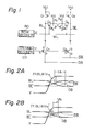
- FIG. 1 partially illustrates the structure of a MIS semiconductor memory device which is the embodiment of the present invention.
- BL and BL designate a pair of bit lines connected to a power source V CC through load transistors Q 1 and Q 2 , respectively.
- Transistors Q3 through Q 6 and resistors R and R 2 constitute a so-called flip-flop type of memory cell, and the transistors Q 3 and Q 4 constitute gate circuits which connect the memory cell and the bit line pair BL and BL.
- the gate of the transistor Q 3 and the gate of the transistor Q 4 are connected to a word line WL which is connected to a row decoder RD.
- the bit lines BL and BL are connected to data buses DB and DB, which constitute a data bus pair, through transistors Q 7 and Q 8 , each of which constitutes a transfer gate, respectively.
- the gate of the transistor Q 7 and the gate of the transistor Q 8 are connected to the output terminal of a column decoder CD.
- the threshold voltage of the gate-source voltage of the transistors Q 7 and Q 8 is lower than that of the enhancement-type transistors used in other circuits of the semiconductor memory device of Fig. 1.
- the threshold voltage of the enhancement-type transistors used in a semiconductor device such as the semiconductor device of Fig. 1 is, for example, 0.7 through 0.9 volt, but the threshold voltage of the transistors Q 7 and Q 8 of Fig. 1 is selected to be a value greater than or equal to zero but less than the above-mentioned values.
- the threshold voltage of the transistors Q 7 and Q 8 is selected to be a value between zero and 0.5 volt.
- the transistors Q 7 and Q 8 are turned on after the output voltage Y of the column decoder CD rises enough so that the difference between the output voltage Y and the voltage of the bit line BL exceeds the threshold voltage of the gate-source voltage of the transistors Q 7 and Q 8 .
- the voltage of the bit line BL and the voltage of the bit line BL are transmitted to the data buses.
- the transistors Q 7 and Q 8 are not turned on until the difference between the output voltage of the column decoder CD and the voltage of the bit line BL becomes relatively large. Therefore, the transistors Q 7 and Q 8 are turned on after a relatively long time has elapsed since the beginning of the rise of the output voltage of the column decoder CD, and thus the access time of the conventional memory device is relatively long.
- the threshold voltage of the transistors Q 7 and Q 8 since the threshold voltage of the transistors Q 7 and Q 8 is low, the difference between the output voltage Y of the column decoder CD and the voltage of the bit line BL is larger than the threshold voltage of the transistors Q 7 and Q 8 a short time after the output voltage Y of the column decoder CD starts to rise, as is illustrated in Fig. 2B. Therefore, the transistors Q 7 and Q 8 are turned on rapidly and changes in the voltage of the bit line BL and the voltage of the bit line BL are rapidly transmitted to the data buses DB and DB so that the time interval td 2 between the intersection of the bit line voltages and the intersection of the data bus voltages is very small.
- the threshold voltage of the transistors Q 7 and Q 8 is relatively small, it is possible to make the mutual conductance gm of each transistor larger than that of each transfer gate transistor of the conventional memory device and to increase the speed of transferring information from the bit lines to the data buses.
- the MIS static-type random access memory device is explained by way of example.
- the present invention is not limited to such a memory device. Rather, it is adaptable to all memory devices comprising transfer gate transistors disposed between bit lines and data buses.
Landscapes
- Engineering & Computer Science (AREA)
- Microelectronics & Electronic Packaging (AREA)
- Computer Hardware Design (AREA)
- Static Random-Access Memory (AREA)
- Read Only Memory (AREA)
- Dram (AREA)
- Semiconductor Memories (AREA)
Applications Claiming Priority (2)
| Application Number | Priority Date | Filing Date | Title |
|---|---|---|---|
| JP57050085A JPS58168272A (ja) | 1982-03-30 | 1982-03-30 | Mis形半導体記憶装置 |
| JP50085/82 | 1982-03-30 |
Publications (3)
| Publication Number | Publication Date |
|---|---|
| EP0090591A2 true EP0090591A2 (de) | 1983-10-05 |
| EP0090591A3 EP0090591A3 (en) | 1984-08-15 |
| EP0090591B1 EP0090591B1 (de) | 1986-07-02 |
Family
ID=12849181
Family Applications (1)
| Application Number | Title | Priority Date | Filing Date |
|---|---|---|---|
| EP83301617A Expired EP0090591B1 (de) | 1982-03-30 | 1983-03-23 | Halbleiter-Speichervorrichtung |
Country Status (4)
| Country | Link |
|---|---|
| EP (1) | EP0090591B1 (de) |
| JP (1) | JPS58168272A (de) |
| DE (1) | DE3364334D1 (de) |
| IE (1) | IE54670B1 (de) |
Cited By (3)
| Publication number | Priority date | Publication date | Assignee | Title |
|---|---|---|---|---|
| EP0554183A3 (de) * | 1992-01-30 | 1994-01-05 | Fujitsu Ltd | |
| US6526473B1 (en) | 1999-04-07 | 2003-02-25 | Samsung Electronics Co., Ltd. | Memory module system for controlling data input and output by connecting selected memory modules to a data line |
| KR100816927B1 (ko) * | 2003-09-30 | 2008-03-25 | 인텔 코오퍼레이션 | 광대역 간섭 상쇄 |
Family Cites Families (1)
| Publication number | Priority date | Publication date | Assignee | Title |
|---|---|---|---|---|
| US4195356A (en) * | 1978-11-16 | 1980-03-25 | Electronic Memories And Magnetics Corporation | Sense line termination circuit for semiconductor memory systems |
-
1982
- 1982-03-30 JP JP57050085A patent/JPS58168272A/ja active Pending
-
1983
- 1983-03-23 DE DE8383301617T patent/DE3364334D1/de not_active Expired
- 1983-03-23 EP EP83301617A patent/EP0090591B1/de not_active Expired
- 1983-03-30 IE IE716/83A patent/IE54670B1/en not_active IP Right Cessation
Cited By (4)
| Publication number | Priority date | Publication date | Assignee | Title |
|---|---|---|---|---|
| EP0554183A3 (de) * | 1992-01-30 | 1994-01-05 | Fujitsu Ltd | |
| US5841704A (en) * | 1992-01-30 | 1998-11-24 | Fujitsu Limited | Static RAM |
| US6526473B1 (en) | 1999-04-07 | 2003-02-25 | Samsung Electronics Co., Ltd. | Memory module system for controlling data input and output by connecting selected memory modules to a data line |
| KR100816927B1 (ko) * | 2003-09-30 | 2008-03-25 | 인텔 코오퍼레이션 | 광대역 간섭 상쇄 |
Also Published As
| Publication number | Publication date |
|---|---|
| JPS58168272A (ja) | 1983-10-04 |
| EP0090591A3 (en) | 1984-08-15 |
| EP0090591B1 (de) | 1986-07-02 |
| IE830716L (en) | 1983-09-30 |
| IE54670B1 (en) | 1990-01-03 |
| DE3364334D1 (en) | 1986-08-07 |
Similar Documents
| Publication | Publication Date | Title |
|---|---|---|
| US5744978A (en) | Variable load device responsive to a circuit parameter | |
| US4464750A (en) | Semiconductor memory device | |
| US4656608A (en) | Semiconductor memory device | |
| EP0388176B1 (de) | Halbleiter-Speichereinrichtung | |
| KR910000388B1 (ko) | 메모리셀 블록의 선택적 동작이 가능한 반도체 메모리장치 | |
| EP0058051B1 (de) | Statische Halbleiterspeicheranordnung | |
| EP0074206B1 (de) | Halbleiterspeicheranordnung | |
| US4634900A (en) | Sense amplifier | |
| JP2885607B2 (ja) | 半導体メモリ | |
| US4433393A (en) | Semiconductor memory device | |
| KR910004733B1 (ko) | 데이타 버스 리셋트 회로를 지닌 반도체 기억장치 | |
| US5260904A (en) | Data bus clamp circuit for a semiconductor memory device | |
| US4779230A (en) | CMOS static ram cell provided with an additional bipolar drive transistor | |
| EP0090591B1 (de) | Halbleiter-Speichervorrichtung | |
| US5317536A (en) | Dual-port type semiconductor integrated memory circuit | |
| EP0262850B1 (de) | Speicherzellschaltung | |
| US5023842A (en) | Semiconductor memory having improved sense amplifiers | |
| US5079745A (en) | Sense amplifier capable of high speed operation | |
| US4821237A (en) | Semiconductor memory device | |
| EP0460619A2 (de) | Halbleiterspeicheranordnung | |
| EP0149403A2 (de) | Leseverstärker für statischen MOS-Speicher | |
| US5138581A (en) | Multiport memory | |
| US6058058A (en) | Memory device with a sense amplifier | |
| KR920008054B1 (ko) | 신호라인에 대한 전송회로 | |
| JPH037962Y2 (de) |
Legal Events
| Date | Code | Title | Description |
|---|---|---|---|
| PUAI | Public reference made under article 153(3) epc to a published international application that has entered the european phase |
Free format text: ORIGINAL CODE: 0009012 |
|
| AK | Designated contracting states |
Designated state(s): DE FR GB |
|
| PUAL | Search report despatched |
Free format text: ORIGINAL CODE: 0009013 |
|
| AK | Designated contracting states |
Designated state(s): DE FR GB |
|
| 17P | Request for examination filed |
Effective date: 19840830 |
|
| GRAA | (expected) grant |
Free format text: ORIGINAL CODE: 0009210 |
|
| AK | Designated contracting states |
Kind code of ref document: B1 Designated state(s): DE FR GB |
|
| ET | Fr: translation filed | ||
| REF | Corresponds to: |
Ref document number: 3364334 Country of ref document: DE Date of ref document: 19860807 |
|
| PLBE | No opposition filed within time limit |
Free format text: ORIGINAL CODE: 0009261 |
|
| STAA | Information on the status of an ep patent application or granted ep patent |
Free format text: STATUS: NO OPPOSITION FILED WITHIN TIME LIMIT |
|
| 26N | No opposition filed | ||
| PGFP | Annual fee paid to national office [announced via postgrant information from national office to epo] |
Ref country code: FR Payment date: 19980310 Year of fee payment: 16 |
|
| PGFP | Annual fee paid to national office [announced via postgrant information from national office to epo] |
Ref country code: GB Payment date: 19980316 Year of fee payment: 16 |
|
| PGFP | Annual fee paid to national office [announced via postgrant information from national office to epo] |
Ref country code: DE Payment date: 19980327 Year of fee payment: 16 |
|
| PG25 | Lapsed in a contracting state [announced via postgrant information from national office to epo] |
Ref country code: GB Free format text: LAPSE BECAUSE OF NON-PAYMENT OF DUE FEES Effective date: 19990323 |
|
| GBPC | Gb: european patent ceased through non-payment of renewal fee |
Effective date: 19990323 |
|
| PG25 | Lapsed in a contracting state [announced via postgrant information from national office to epo] |
Ref country code: FR Free format text: LAPSE BECAUSE OF NON-PAYMENT OF DUE FEES Effective date: 19991130 |
|
| REG | Reference to a national code |
Ref country code: FR Ref legal event code: ST |
|
| PG25 | Lapsed in a contracting state [announced via postgrant information from national office to epo] |
Ref country code: DE Free format text: LAPSE BECAUSE OF NON-PAYMENT OF DUE FEES Effective date: 20000101 |