EP0089898A2 - Pre-adapted module for a high-frequency diode, and method of making the polarisation connection of the diode - Google Patents
Pre-adapted module for a high-frequency diode, and method of making the polarisation connection of the diode Download PDFInfo
- Publication number
- EP0089898A2 EP0089898A2 EP83400588A EP83400588A EP0089898A2 EP 0089898 A2 EP0089898 A2 EP 0089898A2 EP 83400588 A EP83400588 A EP 83400588A EP 83400588 A EP83400588 A EP 83400588A EP 0089898 A2 EP0089898 A2 EP 0089898A2
- Authority
- EP
- European Patent Office
- Prior art keywords
- diode
- connection
- base
- cover
- module
- Prior art date
- Legal status (The legal status is an assumption and is not a legal conclusion. Google has not performed a legal analysis and makes no representation as to the accuracy of the status listed.)
- Granted
Links
Images

Classifications
-
- H—ELECTRICITY
- H01—ELECTRIC ELEMENTS
- H01L—SEMICONDUCTOR DEVICES NOT COVERED BY CLASS H10
- H01L23/00—Details of semiconductor or other solid state devices
- H01L23/02—Containers; Seals
- H01L23/04—Containers; Seals characterised by the shape of the container or parts, e.g. caps, walls
- H01L23/043—Containers; Seals characterised by the shape of the container or parts, e.g. caps, walls the container being a hollow construction and having a conductive base as a mounting as well as a lead for the semiconductor body
-
- H—ELECTRICITY
- H01—ELECTRIC ELEMENTS
- H01L—SEMICONDUCTOR DEVICES NOT COVERED BY CLASS H10
- H01L23/00—Details of semiconductor or other solid state devices
- H01L23/58—Structural electrical arrangements for semiconductor devices not otherwise provided for, e.g. in combination with batteries
- H01L23/64—Impedance arrangements
- H01L23/66—High-frequency adaptations
-
- H—ELECTRICITY
- H01—ELECTRIC ELEMENTS
- H01L—SEMICONDUCTOR DEVICES NOT COVERED BY CLASS H10
- H01L2224/00—Indexing scheme for arrangements for connecting or disconnecting semiconductor or solid-state bodies and methods related thereto as covered by H01L24/00
- H01L2224/01—Means for bonding being attached to, or being formed on, the surface to be connected, e.g. chip-to-package, die-attach, "first-level" interconnects; Manufacturing methods related thereto
- H01L2224/26—Layer connectors, e.g. plate connectors, solder or adhesive layers; Manufacturing methods related thereto
- H01L2224/31—Structure, shape, material or disposition of the layer connectors after the connecting process
- H01L2224/32—Structure, shape, material or disposition of the layer connectors after the connecting process of an individual layer connector
- H01L2224/321—Disposition
- H01L2224/32151—Disposition the layer connector connecting between a semiconductor or solid-state body and an item not being a semiconductor or solid-state body, e.g. chip-to-substrate, chip-to-passive
- H01L2224/32153—Disposition the layer connector connecting between a semiconductor or solid-state body and an item not being a semiconductor or solid-state body, e.g. chip-to-substrate, chip-to-passive the body and the item being arranged next to each other, e.g. on a common substrate
- H01L2224/32175—Disposition the layer connector connecting between a semiconductor or solid-state body and an item not being a semiconductor or solid-state body, e.g. chip-to-substrate, chip-to-passive the body and the item being arranged next to each other, e.g. on a common substrate the item being metallic
- H01L2224/32188—Disposition the layer connector connecting between a semiconductor or solid-state body and an item not being a semiconductor or solid-state body, e.g. chip-to-substrate, chip-to-passive the body and the item being arranged next to each other, e.g. on a common substrate the item being metallic the layer connector connecting to a bonding area protruding from the surface of the item
-
- H—ELECTRICITY
- H01—ELECTRIC ELEMENTS
- H01L—SEMICONDUCTOR DEVICES NOT COVERED BY CLASS H10
- H01L2924/00—Indexing scheme for arrangements or methods for connecting or disconnecting semiconductor or solid-state bodies as covered by H01L24/00
- H01L2924/01—Chemical elements
- H01L2924/01057—Lanthanum [La]
-
- H—ELECTRICITY
- H01—ELECTRIC ELEMENTS
- H01L—SEMICONDUCTOR DEVICES NOT COVERED BY CLASS H10
- H01L2924/00—Indexing scheme for arrangements or methods for connecting or disconnecting semiconductor or solid-state bodies as covered by H01L24/00
- H01L2924/01—Chemical elements
- H01L2924/01079—Gold [Au]
-
- H—ELECTRICITY
- H01—ELECTRIC ELEMENTS
- H01L—SEMICONDUCTOR DEVICES NOT COVERED BY CLASS H10
- H01L2924/00—Indexing scheme for arrangements or methods for connecting or disconnecting semiconductor or solid-state bodies as covered by H01L24/00
- H01L2924/10—Details of semiconductor or other solid state devices to be connected
- H01L2924/11—Device type
- H01L2924/12—Passive devices, e.g. 2 terminal devices
- H01L2924/1203—Rectifying Diode
- H01L2924/12032—Schottky diode
-
- H—ELECTRICITY
- H01—ELECTRIC ELEMENTS
- H01L—SEMICONDUCTOR DEVICES NOT COVERED BY CLASS H10
- H01L2924/00—Indexing scheme for arrangements or methods for connecting or disconnecting semiconductor or solid-state bodies as covered by H01L24/00
- H01L2924/30—Technical effects
- H01L2924/301—Electrical effects
- H01L2924/3011—Impedance
Definitions
- the present invention relates to a method for mounting a microwave diode in order to produce a preadapted module, by using the dimensions of the diode encapsulation box.
- the type of assembly according to the invention applies to avalanche, Gunn, Schottky and other diodes such as varactors, varicap.
- the object of the invention is to encapsulate a diode in a box such that a pre-adapted module is produced, that is to say a module making it possible to adapt the low impedance of the diode to the impedance high from the surrounding environment, usually air.
- the encapsulation is done with a thin dielectric ring, the quartz being particularly suitable, giving a low parasitic capacitance, and a false beam-lead connection in order to minimize the parasitic inductance.
- the shape of the beam-lead also makes it possible to reduce the parasitic capacity.
- the impedance matching is necessary in the microwave, for example in the 94 GHz band, for a diode which must radiate in the space which surrounds it.
- This adaptation is particularly advantageous in a radial form because it can be obtained by means of an ad hoc housing.
- R is negative for an avalanche diode or a Gunn diode, and positive for a Schottky diode or another type.
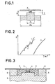
- Figure 1 will help to better understand the importance of impedance matching for the encapsulation of a diode.
- the invention describes the mounting in a housing of a diode patch produced collectively, and with connections such that the radial impedance transformation obtained achieves the goal set, namely of a easy adjustment and clean operation.
- This is obtained on the one hand by means of internal connections to the box in the shape of a metallic star called false beam-lead because the metal bands which constitute the star are not flat but curved, the whole of the star forming in its center a trunk of a pyramid, and on the other hand by means of a quartz ring surrounding the diode patch, this ring having a thickness of less than 120 microns.
- the method of connecting a semiconductor wafer by metal beams known as beam-lead is in itself known, but the beams are very generally flat, this is the case of real beam-lead, which results in a parasitic capacitance effect between the upper connection of the patch and the base on which it is mounted.
- the curved beams which are not parallel to the free surface of the base but which on the contrary move away therefrom, as well as a quartz ring of thickness less than or equal to 120 microns, make that the diode is adapted or sufficiently adapted in impedance to its external environment, and that its power curve as a function of other parameters such as the polarization intensity or the ambient temperature is very clean and without a hitch.
- this type of mounting allows the frequency to be adjusted by slight chemical attack on the patch, before closing the case by thermocompression.
- the invention relates to a preadapted module for microwave diode, comprising a diode patch fixed inside a case consisting of a metal base, a quartz ring and a metal cover, this module being characterized in that that, the base constituting a first connection of the diode, the second connection is constituted by a non-planar metallic star, preformed in the shape of a corolla, the end of the branches of which rests on the face of the quartz ring in contact with the closure cover, and the center of which is in contact with the diode patch, the curvilinear shape of the branches reducing the parasitic inductance and capacitance between this second connection and the base.
- FIG. 3 represents an example of application according to the prior art.
- FIG. 3 represents a part of a case for encapsulating a diode working at microwave frequency.
- a diode patch 4 On a metallic base 3 in copper, gilded and comprising a central pin, is welded a diode patch 4, on which was previously deposited a thickness of gold 5.
- a quartz disk 6 is bonded around the diode patch 4 on the base 3 and the space between the diode pellet 4 and the interior of the quartz disc 6 is filled with a resin 7. Then the assembly is lurked until reappearance by thinning, the thickness d 'gold 5 which has been deposited on the diode pad 4.
- An upper connection 8 being either in the form of a metallic disc or in the form of a metallic star known as true beam-lead is then welded on the thickness of gold 5, that is to say in contact with the diode, and rests at its periphery on the free face of the quartz disc 6.
- the assembly is then covered with a cover, not shown in this figure or encapsulated in a more complex cavity if necessary.
- connection 8 which is a metal strip or plate is parallel to the face of the base on which the diode is mounted and thus has a certain parasitic capacity, which is not negligible at the frequency of diode work.
- this type of encapsulation is unitary, requires prowling, and is therefore long, costly and not very industrial.
- the diode is mounted without the possibility of subsequent adjustment, for example by chemical thinning, by a slight acid attack, since the diode is in fact embedded inside a resin 7 and protected on its two faces by the base of copper 3 and by the thickness of gold 5: since an adjustment is not possible once the encapsulation operation is carried out, the adjustment or adaptation in frequency is also not possible.
- FIG. 4 represents a diode encapsulated in a case according to the invention, and adapted or pre-adapted sufficiently in impedance.
- the patch 4 of the diode equipped with a gold strip 9 serving as an integrated radiator, the assembly 4 and 9 being cut from a washer which contains a very large number thereof, is firstly attached to a base 3 in nickel-plated and gilded copper, generally by brazing or thermocompression of the lamella 9.
- a quartz ring 6 is thermo - compressed, glued or welded to the base 3 at the joint 12, then the upper connection 10 in the form of a false beam -lead is attached to the diode patch: it rests on the upper face 13 of the quartz ring 6, and L the assembly is closed by a metal cover 11 also thermocompressed, bonded or brazed on the face upper of the quartz ring.
- connection 10 of the diode is, as has already been said, in the form of a metallic star whose branches are not planar, but move away from the base 3, which reduces the parasitic inductance and the parasitic capacity.
- the fact that the polarization connection 10 is in the form of a star allows, when the diode has been fixed on the base and before the cover 11 is attached, to adjust the oscillation frequency of the device by means of a slight chemical attack, which makes it possible to reduce the diameter of the diode patch, the introduction of the reactive liquid being possible since the connection 10 has orifices between the arms of the star.
- a pellet of semiconductor such as an Impatt microwave diode to operate at 94 GHz has a diameter of 35 microns, a thickness of 5 microns and is thermocompressed on a gold coin 9, 200 microns side and 50 microns thickness.
- the quartz ring 6, metallized on its two faces 12 and 13, has an outside diameter between 750 and 800 microns, an inside diameter between 400 and 450 microns, and a thickness of the order of 100 microns if the copper base 3 is flat, or of the order of 150 microns if base 3 has a stud on which the diode is fixed.
- a deposit 18 of chromium / gold is produced in FIG. 7 on the mesa thus formed. Then after photomasking to obtain the desired star shape, an electrolytic growth of gold 19, 2 microns thick, is carried out, which makes it possible to form the connections in the form of a false beam-lead with several branches.
- the last operation to recover pieces 10 having a shape flared and a star design consists in chemically attacking the chromium gold / 18 not masked and what remains of the silicon 14 which was initially used to form a mesa.
- FIG. 8 represents such a connection, and highlights the star shape which does not appear in FIG. 7.
- the central part 20 of this false beam-lead is that which is thermocompressed on the diode pad, while the end of each branch 21 is that which is thermocompressed on the metallized face 13 of the quartz disc 6.
- the star of FIG. 8 is represented with 6 branches, and the number of branches is not determinative of the invention, since what is important is to make a metallic connection which is not planar so as to move away of the substrate, and which allows a liquid such as an acid to circulate between the star branches so as to be able to attack chemically the semiconductor wafer.
- Figure 8 is shown a particularly well adapted form of flared beam-lead, that is to say that each star branch becomes wider and wider as we get closer of the outer contour of the encapsulation box: this solution makes it possible to reduce the connection self.
- other star designs with branches constituted by bands the sides of which are or are not parallel to each other, or with a different number of branches fall within the scope of the invention.
- the false beam-lead of FIG. 8 has of the order of 720 microns in diameter; each of these branches is 230 microns long by 120 microns wide in its rectangular part and. the core 20 of this metallic star 50 microns aside: it is not possible to produce such a part, for example by stamping a gold leaf.
- the false beam-lead connection 10 includes, coming from manufacturing, a seal 22 which joins together the different branches 21 of the false beam-lead.
- This seal makes it possible, when the case has been closed by thermocompression, to more easily ensure perfect sealing between the branches of the false beam-lead, and consequently the absence of any leaks at the level of the cover 11.
- the microwave diode mounting method according to the invention therefore makes it possible to obtain a semiconductor, adjustable in frequency by a chemical process, since it is not coated with a polymer or a resin, and whose radial impedance transformation is effected by the very dimensions of the case, it can be thermocompressed, and not glued as is generally done.
Landscapes
- Physics & Mathematics (AREA)
- Condensed Matter Physics & Semiconductors (AREA)
- General Physics & Mathematics (AREA)
- Engineering & Computer Science (AREA)
- Computer Hardware Design (AREA)
- Microelectronics & Electronic Packaging (AREA)
- Power Engineering (AREA)
- Structures Or Materials For Encapsulating Or Coating Semiconductor Devices Or Solid State Devices (AREA)
- Wire Bonding (AREA)
- Lead Frames For Integrated Circuits (AREA)
Abstract
L'invention concerne un montage de diode hyperfréquence, en vue de réaliser un module préadapté. Le module selon l'invention comprend une embase (3) en cuivre, un anneau de quartz (6) et un capot (11) en cuivre: ces trois pièces, dorées au moins sur leurs faces en regard, sont assemblées par thermocompression (12,13). A l'intérieur de ce boitier, la pastille de diode (4), soudée sur l'embase (3) par l'intermédiaire d'un radiateur d'or (9) est polarisée par une connexion en faux "beam-lead" (10), étoile métallique dont les branches sont incurvées, ce qui diminue l'inductance et la capacité de cette connexion par rapport à l'embase. Le faux "beam-lead" est réalisé par métallisation d'un mésa obtenu sur une tranche de silicium. Application aux systèmes fonctionnant en hyperfréquences, notamment dans le domaine des hyperfréquences.The invention relates to a microwave diode assembly, in order to produce a pre-adapted module. The module according to the invention comprises a base (3) made of copper, a quartz ring (6) and a cover (11) made of copper: these three pieces, gilded at least on their opposite faces, are assembled by thermocompression (12 , 13). Inside this box, the diode patch (4), welded to the base (3) via a gold radiator (9) is polarized by a false "beam-lead" connection (10), metal star whose branches are curved, which reduces the inductance and the capacity of this connection relative to the base. The false "beam-lead" is produced by metallization of a mesa obtained on a silicon wafer. Application to systems operating at microwave frequencies, in particular in the microwave domain.
Description
La présente invention concerne un procédé de montage de diode hyperfréquence en vue de réaliser un module préadapté, par utilisation des dimensions du boitier d'encapsulation de la diode. Le type de montage selon l'invention s'applique aux diodes à avalanche, Gunn, Schottky et autres telles que varactors, varicap. L'objet de l'invention est d'encapsuler une diode dans un boitier tel que l'on réalise un module préadapté, c'est-à-dire un module permettant d'adapter l'impédance faible de la diode à l'impédance élevée du milieu environnant, généralement l'air. L'encapsulation est faite avec un anneau de diélectrique mince, le quartz convenant particulièrement bien, donnant une faible capacité parasite, et une connexion de type faux beam-lead afin de minimiser l'inductance parasite. La forme du beam-lead permet également de réduire la capacité parasite.The present invention relates to a method for mounting a microwave diode in order to produce a preadapted module, by using the dimensions of the diode encapsulation box. The type of assembly according to the invention applies to avalanche, Gunn, Schottky and other diodes such as varactors, varicap. The object of the invention is to encapsulate a diode in a box such that a pre-adapted module is produced, that is to say a module making it possible to adapt the low impedance of the diode to the impedance high from the surrounding environment, usually air. The encapsulation is done with a thin dielectric ring, the quartz being particularly suitable, giving a low parasitic capacitance, and a false beam-lead connection in order to minimize the parasitic inductance. The shape of the beam-lead also makes it possible to reduce the parasitic capacity.
L'adaptation d'impédance est nécessaire en hyperfréquence, par exemple dans la bande 94 GHz, pour une diode qui doit rayonner dans l'espace qui l'entoure. Cette adaptation est particulièrement intéressante sous une forme radiale car elle peut être obtenue grâce à un boitier ad hoc. Au niveau de la pastille de semi-conducteur, une diode dans le cas présent, l'impédance que présente celle-ci est du type R + jX, dans lequel R représente la partie réelle de la résistance de la diode et X la partie imaginaire de cette résistance, j étant égal par définition à j2 = -1 et est représentatif des imaginaires. R est négatif pour une diode à avalanche ou une diode Gunn, et positif pour une diode Schottky ou d'un autre type. La figure 1 aidera à mieux comprendre l'importance de l'adaptation d'impédance pour l'encapsu- lation d'une diode.The impedance matching is necessary in the microwave, for example in the 94 GHz band, for a diode which must radiate in the space which surrounds it. This adaptation is particularly advantageous in a radial form because it can be obtained by means of an ad hoc housing. At the level of the semiconductor chip, a diode in the present case, the impedance which this presents is of the type R + jX, in which R represents the real part of the resistance of the diode and X the imaginary part of this resistance, j being by definition equal to j2 = -1 and is representative of the imaginary. R is negative for an avalanche diode or a Gunn diode, and positive for a Schottky diode or another type. Figure 1 will help to better understand the importance of impedance matching for the encapsulation of a diode.
Sur cette figure 1, soit A la diode dans laquelle la pastille de semiconducteur est soudée sur une embase métallique et comporte une connexion supérieure. Soit Øi diamètre du plot métallique sur lequel est soudée la diode A, Øe diamètre de l'embase, c'est-à-dire également le diamètre intérieur de la cavité, soit B la distance qui sépare la connexion supérieure de l'embase et C l'épaisseur de la diode, ou encore la distance qui sépare la connexion supérieure du plot sur lequel est soudée la pastille. La pastille de diode est entourée d'un diélectrique de constante donnée, ou de plusieurs diélectriques de constantes différentes qui donnent une constante équivalente moyenne. Selon les cas, le diélectrique qui entoure la pastille est soit de l'air soit un isolant sous forme de résine. On démontre que l'impédance de l'espace entourant la diode ayant une valeur R + jX ramené à la périphérie, il existe un ensemble unique de valeurs de Øi, Øe, B, C tel qu'il y a adaptation d'impédance du dispositif semiconducteur, soit :![]()
![]()
Cependant, dans la pratique, il suffit que k1R et k2X s'approchent suffisamment de R et X car alors les accords mécaniques classiques dans la monture deviennent extrêmement aisés ; c'est pourquoi l'on dit préadaptation et non pas adaptation.However, in practice, it suffices that k 1 R and k 2 X come close enough to R and X because then the conventional mechanical chords in the frame become extremely easy; this is why we say pre-adaptation and not adaptation.
Cette transformation d'impédance est extrêmement intéressante en particulier pour les diodes à avalanche, car elle simplifie considérablement la cavité : par exemple la polarisation sur l'électrode supérieure peut être réalisée par un simple fil fin. En outre et ceci est montré sur la figure 2, la courbe de la puissance délivrée en fonction d'une autre variable telle que le courant de polarisation I ou la température ambiante T, est très propre et sans hystérésis, ou sans accroc. Ainsi sur la figure 2, la courbe 1 représente la courbe de puissance de diodes encapsulées dans un boitier sans adaptation d'impédance : cette courbe ne connaît pas une variation régulière, mais au contraire présente des décrochages, ceux-ci variant de plus d'une diode à l'autre selon le boitier. Au contraire la courbe 2 qui présente une variation très régulière correspond à une diode correctement encapsulée dans un boitier avec adaptation d'impédance.This impedance transformation is extremely advantageous, in particular for avalanche diodes, because it considerably simplifies the cavity: for example, the polarization on the upper electrode can be achieved by a simple fine wire. Furthermore and this is shown in FIG. 2, the curve of the power delivered as a function of another variable such as the bias current I or the ambient temperature T, is very clean and without hysteresis, or without snag. Thus in FIG. 2, curve 1 represents the power curve of diodes encapsulated in a case without adaptation of impedance: this curve does not experience a regular variation, but on the contrary presents dropouts, these varying by more than one diode to another depending on the case. On the contrary the curve 2 which presents a very regular variation corresponds to a diode correctly encapsulated in a case with adaptation of impedance.
Ceci montre l'importance qu'il y a, surtout à de telles fréquences proches de 100 GHz, à ce qu'une pastille de diode soit correctement encapsulée et montée dans son boitier, qui fait cavité, tout ceci de préférence à partir de pièces réalisées de façon collective de façon à être plus industriel.This shows the importance that there is, especially at such frequencies close to 100 GHz, that a diode patch is correctly encapsulated and mounted in its housing, which forms a cavity, all this preferably from parts. carried out collectively so as to be more industrial.
L'invention décrit le montage dans un boitier d'une pastille de diode réalisée de façon collective, et avec des connexions telle que la transformation radiale d'impédance obtenue atteigne le but fixé à savoir d'un réglage aisé et d'un fonctionnement propre. Ceci est obtenu d'une part au moyen de connexions internes au boitier en forme d'étoile métallique dite faux beam-lead parce que les bandes de métal qui constituent l'étoile ne sont pas planes mais incurvées, l'ensemble de l'étoile formant en son centre un tronc de pyramide, et d'autres part au moyen d'un anneau de quartz entourant la pastille de diodes, cet anneau ayant une épaisseur inférieure à 120 microns. Le procédé de connexion d'une pastille de semiconducteur par poutres métalliques dit beam-lead est en soit connu, mais les poutres sont très généralement planes, c'est le cas du vrai beam-lead, ce qui entraîne un effet de capacité parasite entre la connexion supérieure de la pastille et l'embase sur laquelle celle-ci est montée. Les poutres incurvées qui ne sont pas parallèles à la surface libre de l'embase mais qui au contraire s'en éloignent, ainsi qu'un anneau de quartz d'épaisseur inférieure ou égale à 120 microns, font que la diode est adaptée ou suffisamment adaptée en impédance à son environnement extérieur, et que sa courbe de puissance en fonction d'autres paramètres telle que l'intensité de polarisation ou la température ambiante est très propre et sans accroc. De plus ce type de montage permet un ajustage de la fréquence par légère attaque chimique de la pastille, avant fermeture du boitier par thermocompression.The invention describes the mounting in a housing of a diode patch produced collectively, and with connections such that the radial impedance transformation obtained achieves the goal set, namely of a easy adjustment and clean operation. This is obtained on the one hand by means of internal connections to the box in the shape of a metallic star called false beam-lead because the metal bands which constitute the star are not flat but curved, the whole of the star forming in its center a trunk of a pyramid, and on the other hand by means of a quartz ring surrounding the diode patch, this ring having a thickness of less than 120 microns. The method of connecting a semiconductor wafer by metal beams known as beam-lead is in itself known, but the beams are very generally flat, this is the case of real beam-lead, which results in a parasitic capacitance effect between the upper connection of the patch and the base on which it is mounted. The curved beams which are not parallel to the free surface of the base but which on the contrary move away therefrom, as well as a quartz ring of thickness less than or equal to 120 microns, make that the diode is adapted or sufficiently adapted in impedance to its external environment, and that its power curve as a function of other parameters such as the polarization intensity or the ambient temperature is very clean and without a hitch. In addition, this type of mounting allows the frequency to be adjusted by slight chemical attack on the patch, before closing the case by thermocompression.
De façon plus précise l'invention concerne un module préadapté pour diode hyperfréquence, comportant une pastille de diode fixée à l'intérieur d'un boitier constitué par une embase métallique, un anneau de quartz et un capot métallique, ce module étant caractérisé en ce que, l'embase constituant une première connexion de la diode, la seconde connexion est constituée par une étoile métallique, non plane, préformée en forme de corolle, dont l'extrémité des branches s'appuie sur la face de l'anneau de quartz en contact avec le capot de fermeture, et dont le centre est en contact avec la pastille de la diode, la forme curviligne des branches réduisant l'inductance et la capacité parasites entre cette seconde connexion et l'embase.More precisely, the invention relates to a preadapted module for microwave diode, comprising a diode patch fixed inside a case consisting of a metal base, a quartz ring and a metal cover, this module being characterized in that that, the base constituting a first connection of the diode, the second connection is constituted by a non-planar metallic star, preformed in the shape of a corolla, the end of the branches of which rests on the face of the quartz ring in contact with the closure cover, and the center of which is in contact with the diode patch, the curvilinear shape of the branches reducing the parasitic inductance and capacitance between this second connection and the base.
L'invention sera mieux comprise par la desription d'un exemple d'application, laquelle s'appuie sur les figures annexées qui représentent :
- - figure 1 : schéma d'adaptation d'impédance d'une diode à l'espace l'entourant.
- - figure 2 : courbe de puissance d'une diode en fonction de sa transformation impédance.
- - figure 3 : une diode encapsulée et adaptée en impédance selon l'art antérieur.
- - figure 4 : une diode encapsulée et adaptée en impédance selon l'invention
- - figures 5 à 8 : étapes de fabrication d'un faux beam-lead.
- - Figure 1: diagram of impedance adaptation of a diode to the surrounding space.
- - Figure 2: power curve of a diode as a function of its impedance transformation.
- - Figure 3: an encapsulated diode and adapted in impedance according to the prior art.
- - Figure 4: an encapsulated diode and adapted in impedance according to the invention
- - Figures 5 to 8: stages of manufacturing a false beam-lead.
A partir des raisons fondamentales, exposées en s'appuyant sur les figures 1 et 2, qui montrent l'intérêt de l'adaptation d'impédance d'une diode à son boitier d'encapsulation, la figure 3 représente un exemple d'application selon l'art antérieur.Starting from the fundamental reasons, exposed by relying on FIGS. 1 and 2, which show the advantage of the impedance adaptation of a diode to its encapsulation box, FIG. 3 represents an example of application according to the prior art.
Une approche de ces problèmes d'adaptation d'impédance a déjà été faite par la Demanderesse qui en particulier a déposé les demandes de brevet N° 76 11 442 du 16 Avril 1976 et N° 78 07 800 du 17 Mars 1978. Ces demandes de brevet décrivent des procédés de montage qui en fait ne sont pas suffisamment industriels pour beaucoup d'applications.An approach to these impedance matching problems has already been made by the Applicant who in particular filed patent applications No. 76 11 442 of April 16, 1976 and No. 78 07 800 of March 17, 1978. These applications for Patents describe mounting methods which in fact are not industrial enough for many applications.
La figure 3 représente une partie d'un boitier d'encapsulation d'une diode travaillant en hyperfréquence. Sur une embase métallique 3 en cuivre, doré et comportant un picot central, est soudée une pastille de diode 4, sur laquelle a été déposée auparavant une épaisseur d'or 5. Un disque de quartz 6 est collé autour de la pastille de diode 4 sur l'embase 3 et l'espace compris entre la pastille de diode 4 et l'intérieur du disque de quartz 6 est remplie par une résine 7. Puis l'ensemble est rôdé jusqu'à faire réapparaître par amincissement, l'épaisseur d'or 5 qui a été déposée sur la pastille de diode 4. Une connexion supérieure 8, se présentant soit sous la forme d'un disque métallique soit sous la forme d'une étoile métallique dite vrai beam-lead est alors soudée sur l'épaisseur d'or 5, c'est-à-dire en contact avec la diode, et repose à sa périphérie sur la face libre du disque de quartz 6. L'ensemble est ensuite recouvert d'un capot, non représenté sur cette figure ou encapsulé dans une cavité plus complexe si nécessaire.FIG. 3 represents a part of a case for encapsulating a diode working at microwave frequency. On a
Ce type de montage selon l'art connu présente plusieurs inconvénients. En premier lieu, la connexion 8 qui est un ruban ou une plaque métallique est parallèle à la face de l'embase sur laquelle est montée la diode et présente ainsi une certaine capacité parasite, non négligeable à la fréquence de travail de la diode. Et surtout en second lieu, ce type d'encapsulation est unitaire, nécessite un rôdage, et est donc longue, coûteuse et peu industrielle. Enfin la diode est montée sans possibilité de réglage ultérieur, par exemple par amincissement chimique, par une légère attaque acide, puisque la diode est en fait noyée à l'intérieur d'une résine 7 et protégée sur ses deux faces par l'embase de cuivre 3 et par l'épaisseur d'or 5 : puisqu'un ajustage n'est pas possible une fois que l'opération d'encapsulation est effectuée, le réglage ou l'adaptation en fréquence n'est pas non plus possible.This type of assembly according to the known art has several drawbacks. Firstly, the connection 8 which is a metal strip or plate is parallel to the face of the base on which the diode is mounted and thus has a certain parasitic capacity, which is not negligible at the frequency of diode work. And above all secondly, this type of encapsulation is unitary, requires prowling, and is therefore long, costly and not very industrial. Finally the diode is mounted without the possibility of subsequent adjustment, for example by chemical thinning, by a slight acid attack, since the diode is in fact embedded inside a
La figure 4 représente une diode encapsulée dans un boitier selon l'invention, et adaptée ou préadaptée suffisamment en impédance.FIG. 4 represents a diode encapsulated in a case according to the invention, and adapted or pre-adapted sufficiently in impedance.
La pastille 4 de la diode équipée d'une lamelle d'or 9 servant de radiateur intégré, l'ensemble 4 et 9 étant découpé dans une rondelle qui en contient un très grand nombre, est tout d'abord rapportée sur une embase 3 en cuivre nickelé et doré, généralement par brasure ou par thermocompression de la lamelle 9. Un anneau de quartz 6 est thermo-comprimé, collé ou soudé sur l'embase 3 au niveau du joint 12, puis la connexion supérieure 10 en forme de faux beam-lead est rapportée sur la pastille de la diode : elle s'appuie sur la face supérieure 13 de l'anneau de quartz 6, et L l'ensemble est refermé par un couvercle métallique 11 lui aussi thermocomprimé, collé ou brasé sur la face supérieure de l'anneau de quartz.The
La connexion 10 de la diode est, comme cela a déjà été dit, en forme d'étoile métallique dont les branches ne sont pas planes, mais s'éloignent de l'embase 3, ce qui diminue l'inductance et la capacité parasites. Le fait que la connexion de polarisation 10 se présente sour la forme d'une étoile permet, lorsque la diode a été fixée sur l'embase et avant que le couvercle 11 ne soit rapporté, de procéder à un réglage de fréquence d'oscillation du dispositif au moyen d'une légère attaque chimique, qui permet de réduire le diamètre de la pastille de diode, l'introduction du liquide réactif étant possible puisque la connexion 10 présente des orifices entre les bras de l'étoile.The
La réalisation de ce type de montage présente peu de difficultés malgré les dimensions très petites de l'ensemble. A titre d'illustration, non limitative de l'invention, après découpe dans une rondelle, une pastille de semi-conducteur telle qu'une diode hyperfréquence Impatt devant fonctionner à 94 GHz a un diamètre de 35 microns, une épaisseur de 5 microns et se trouve thermocomprimée sur une pièce d'or 9, de 200 microns de côté et de 50 microns d'épaisseur. L'anneau de quartz 6, métallisé sur ses deux faces 12 et 13, a un diamètre extérieur compris entre 750 et 800 microns, un diamètre intérieur compris entre 400 et 450 microns, et une épaisseur de l'ordre de 100 microns si l'embase de cuivre 3 est plane, ou de l'ordre de 150 microns si l'embase 3 comporte un plot sur lequel est fixée la diode. Ces dimensions sont citées afin de mettre en évidence la difficulté qu'il y a à réaliser une étoile métallique qui ne soit pas plane : sa fabrication échappe aux techniques connues de la métallurgie et est expliquée au moyen des figures 5 à 8.The realization of this type of assembly presents few difficulties despite the very small dimensions of the assembly. By way of illustration, without limitation of the invention, after cutting from a washer, a pellet of semiconductor such as an Impatt microwave diode to operate at 94 GHz has a diameter of 35 microns, a thickness of 5 microns and is thermocompressed on a gold coin 9, 200 microns side and 50 microns thickness. The
Pour réaliser une étoile en faux beam-lead, telle que la connexion 10 de la figure 4 il est nécessaire de réaliser d'abord une matrice à partir d'une tranche de silicium - figure 5 - sur laquelle sont déposées successivement une couche de silice Si 02 de 0,2 micron d'épaisseur, une couche de nitrure de silicium Si3N4 de 0,15 micron d'épaisseur et une couche de silice Si 02 de 0,2 micron d'épaisseur. La figure 6 représente l'étape suivante de réalisation du faux beam-lead. Sur la précédente tranche de silicium 14 recouverte par ces trois couches de protection 15, on définit par photomasquage des zones 16, puis on attaque chimiquement les couches de protection 15 jusqu'à mettre à nu la tranche de silicium 14. En poursuivant l'attaque chimique, le silicium est à son tour attaqué et comme l'attaque chimique se prolonge sous les couches de protection 15, on obtient à l'issue de cette opération un mésa dont les deux flancs 17 ont une forme légèrement arrondie, qui donne ainsi une forme en corolle.To make a false beam-lead star, such as the
L'ensemble des couches de protection 15 et de la couche de résine de photomasquage 16 sont alors supprimées.All the
Après élimination de ces couches de protection, on réalise - figure 7 - un dépôt 18 de chrome/or sur le mésa ainsi formé. Puis après photomasquage pour obtenir la forme d'étoile désirée, on effectue une croissance électrolytique d'or 19, d'une épaisseur de 2 microns, ce qui permet de former les connexions en forme de faux beam-lead à plusieurs branches.After removal of these protective layers, a deposit 18 of chromium / gold is produced in FIG. 7 on the mesa thus formed. Then after photomasking to obtain the desired star shape, an electrolytic growth of
La dernière opération pour récupérer des pièces 10 ayant une forme évasée et un dessin d'étoile consiste à attaquer chimiquement le chrome or/18 non masqué et ce qui reste du silicium 14 qui a initialement servi à former un mésa.The last operation to recover
La figure 8 représente une telle connexion, et met en évidence la forme d'étoile qui n'apparaît pas sur la figure 7. La partie centrale 20 de ce faux beam-lead est celle qui est thermocomprimée sur la pastille de diode, tandis que l'extrémité de chaque branche 21 est celle qui est thermocomprimée sur la face métallisée 13 du disque de quartz 6.FIG. 8 represents such a connection, and highlights the star shape which does not appear in FIG. 7. The
L'étoile de la figure 8 est représentée avec 6 branches, et le nombre de branches n'est pas déterminatif de l'invention, puisque ce qui est important est de réaliser une connexion métallique qui ne soit pas plane de façon à s'éloigner du substrat, et qui permette à un liquide tel qu'un acide de circuler entre les branches d'étoile de façon à pouvoir attaquer chimiquement la pastille semiconductrice. De plus, sur la figure 8 est représentée une forme particulièrement bien adaptée de beam-lead évasé, c'est-à-dire que chaque branche d'étoile devient de plus en plus large au fur et à mesure que l'on se rapproche du contour extérieur du boitier d'encapsulation : cette solution permet de diminuer la self de la connexion. Cependant d'autres dessins d'étoile avec des branches constituées par des bandes dont les côtés sont ou non parallèles entre eux, ou avec un nombre de branches différent entrent dans le domaine de l'invention.The star of FIG. 8 is represented with 6 branches, and the number of branches is not determinative of the invention, since what is important is to make a metallic connection which is not planar so as to move away of the substrate, and which allows a liquid such as an acid to circulate between the star branches so as to be able to attack chemically the semiconductor wafer. In addition, in Figure 8 is shown a particularly well adapted form of flared beam-lead, that is to say that each star branch becomes wider and wider as we get closer of the outer contour of the encapsulation box: this solution makes it possible to reduce the connection self. However, other star designs with branches constituted by bands the sides of which are or are not parallel to each other, or with a different number of branches fall within the scope of the invention.
A titre d'exemple, et sans que ceci soit limitatif de l'invention, mais plutôt pour montrer la difficulté qu'il y aurait à façonner une telle pièce par d'autres procédés métallurgiques, le faux beam-lead de la figure 8 a de l'ordre de 720 microns de diamètre ; chacune de ces branches a 230 microns de longueur sur 120 microns de largeur dans sa partie rectangulaire et. le coeur 20 de cette étoile métallique à 50 microns de côté : il n'est pas possible de réaliser une telle pièce par exemple par emboutissage d'une feuille d'or.By way of example, and without this being limiting of the invention, but rather to show the difficulty that there would be in shaping such a part by other metallurgical processes, the false beam-lead of FIG. 8 has of the order of 720 microns in diameter; each of these branches is 230 microns long by 120 microns wide in its rectangular part and. the
Lorsque cette connexion en forme de faux beam-lead est fixée par thermocompression sur la pastille semiconductrice 4 de la figure 4, il est possible de tester les pastilles en fréquence avant de refermer le boitier par un couvercle 11 de cuivre nickelé et doré. Si la fréquence n'est pas exactement celle qui est désirée, et compte-tenu du diamètre du capot 11 qui fixe la fréquence d'oscillation du module préaccordé, en contribuant à la tranformation radiale d'impédance, il est alors possible d'effectuer une légère attaque chimique de la pastille 4 par introduction d'acide entre les branches de l'étoile de faux beam-lead 10 et rinçage. La fréquence étant ajustée au mieux le couvercle 11 est rapporté sur la rondelle de quartz 6 et l'encapsulation est achevée et étanche.When this false beam-lead connection is fixed by thermocompression on the
Eventuellement, et dans le but d'assurer une parfaite étanchéité entre la rondelle de quartz 6 et le capot 11, la connexion en faux beam-lead 10 comporte, venant de fabrication, un joint 22 qui réunit entre elle les différentes branches 21 du faux beam-lead. Ce joint permet lorsque le boitier a été fermé par thermocompression d'assurer plus facilement une étanchéité parfaite entre les branches du faux beam-lead, et par conséquent l'absence de toutes fuites au niveau du couvercle 11.Optionally, and in order to ensure a perfect seal between the
Le procédé de montage de diode hyperfréquence selon l'invention permet donc d'obtenir un semiconducteur, ajustable en fréquence par un procédé chimique, car il n'est pas enrobé par un polymère ou une résine, et dont la transformation radiale d'impédance est effectuée par les dimensions mêmes du boitier, celui-ci pouvant être thermocomprimé, et non pas collé comme cela se fait généralement. Cette invention est précisée par les revendications ci-après.The microwave diode mounting method according to the invention therefore makes it possible to obtain a semiconductor, adjustable in frequency by a chemical process, since it is not coated with a polymer or a resin, and whose radial impedance transformation is effected by the very dimensions of the case, it can be thermocompressed, and not glued as is generally done. This invention is further clarified by the claims below.
Claims (6)
Applications Claiming Priority (2)
| Application Number | Priority Date | Filing Date | Title |
|---|---|---|---|
| FR8204920 | 1982-03-23 | ||
| FR8204920A FR2524202B1 (en) | 1982-03-23 | 1982-03-23 | PRE-ADAPTED MODULE FOR MICROWAVE, AND METHOD FOR MAKING THE POLARIZATION CONNECTION OF THE DIODE |
Publications (3)
| Publication Number | Publication Date |
|---|---|
| EP0089898A2 true EP0089898A2 (en) | 1983-09-28 |
| EP0089898A3 EP0089898A3 (en) | 1984-02-22 |
| EP0089898B1 EP0089898B1 (en) | 1986-10-15 |
Family
ID=9272292
Family Applications (1)
| Application Number | Title | Priority Date | Filing Date |
|---|---|---|---|
| EP83400588A Expired EP0089898B1 (en) | 1982-03-23 | 1983-03-22 | Pre-adapted module for a high-frequency diode, and method of making the polarisation connection of the diode |
Country Status (6)
| Country | Link |
|---|---|
| US (1) | US4864384A (en) |
| EP (1) | EP0089898B1 (en) |
| JP (1) | JPS58170042A (en) |
| CA (1) | CA1206275A (en) |
| DE (1) | DE3367043D1 (en) |
| FR (1) | FR2524202B1 (en) |
Families Citing this family (8)
| Publication number | Priority date | Publication date | Assignee | Title |
|---|---|---|---|---|
| US5334872A (en) * | 1990-01-29 | 1994-08-02 | Mitsubishi Denki Kabushiki Kaisha | Encapsulated semiconductor device having a hanging heat spreading plate electrically insulated from the die pad |
| US5202288A (en) * | 1990-06-01 | 1993-04-13 | Robert Bosch Gmbh | Method of manufacturing an electronic circuit component incorporating a heat sink |
| DE4209983A1 (en) * | 1992-03-27 | 1993-09-30 | Daimler Benz Ag | Semiconductor component mfr. esp. IMPATT diode prodn. - producing component, housing and connection contacts in integrated construction from and on semiconductor substrate |
| US5550403A (en) * | 1994-06-02 | 1996-08-27 | Lsi Logic Corporation | Improved laminate package for an integrated circuit and integrated circuit having such a package |
| US7449780B2 (en) * | 2003-03-31 | 2008-11-11 | Intel Corporation | Apparatus to minimize thermal impedance using copper on die backside |
| US20050127121A1 (en) * | 2003-12-15 | 2005-06-16 | George Wells | Quick release holster |
| JP4690938B2 (en) * | 2006-05-16 | 2011-06-01 | 株式会社東芝 | High frequency element module |
| CN104795453B (en) * | 2015-04-24 | 2018-06-12 | 中国电子科技集团公司第十三研究所 | A kind of more beam lead GaAs base schottky frequency doubled diodes |
Citations (2)
| Publication number | Priority date | Publication date | Assignee | Title |
|---|---|---|---|---|
| FR2284195A1 (en) * | 1974-09-03 | 1976-04-02 | Hughes Aircraft Co | INTEGRATED CIRCUIT FOR MILLIMETRIC WAVES |
| US3974518A (en) * | 1975-02-21 | 1976-08-10 | Bell Telephone Laboratories, Incorporated | Encapsulation for high frequency semiconductor device |
Family Cites Families (5)
| Publication number | Priority date | Publication date | Assignee | Title |
|---|---|---|---|---|
| SE373689B (en) * | 1973-06-12 | 1975-02-10 | Asea Ab | SEMICONDUCTOR DEVICE CONSISTING OF A THYRISTOR WITH CONTROL POWER, WHICH SEMICONDUCTOR DISC IS INCLUDED IN A BOX |
| US3894895A (en) * | 1973-10-29 | 1975-07-15 | Trw Inc | Mesa etching without overhang for semiconductor devices |
| JPS52142968A (en) * | 1976-05-24 | 1977-11-29 | Fujitsu Ltd | Assembling method of semiconductor devices |
| JPS5481271U (en) * | 1977-11-18 | 1979-06-08 | ||
| US4415025A (en) * | 1981-08-10 | 1983-11-15 | International Business Machines Corporation | Thermal conduction element for semiconductor devices |
-
1982
- 1982-03-23 FR FR8204920A patent/FR2524202B1/en not_active Expired
-
1983
- 1983-03-21 CA CA000424111A patent/CA1206275A/en not_active Expired
- 1983-03-22 DE DE8383400588T patent/DE3367043D1/en not_active Expired
- 1983-03-22 EP EP83400588A patent/EP0089898B1/en not_active Expired
- 1983-03-22 JP JP58047787A patent/JPS58170042A/en active Granted
-
1987
- 1987-04-10 US US07/037,128 patent/US4864384A/en not_active Expired - Fee Related
Patent Citations (2)
| Publication number | Priority date | Publication date | Assignee | Title |
|---|---|---|---|---|
| FR2284195A1 (en) * | 1974-09-03 | 1976-04-02 | Hughes Aircraft Co | INTEGRATED CIRCUIT FOR MILLIMETRIC WAVES |
| US3974518A (en) * | 1975-02-21 | 1976-08-10 | Bell Telephone Laboratories, Incorporated | Encapsulation for high frequency semiconductor device |
Non-Patent Citations (2)
| Title |
|---|
| NACHRICHTEN ELEKTRONIK, vol. 33, no. 4, avril 1979 HEIDELBERG (DE) "Millimeterwellen-Halbleiter und Systeme Teil 2", pages 118-123. * |
| POEE JOURNAL, vol. 72, no. 4, janvier 1980 LONDRES (GB) M. PILGRIM et al.: "An IMPATT Diode Amplifier for 11 GHz Digital Radio-Relay Systems", pages 220-227. * |
Also Published As
| Publication number | Publication date |
|---|---|
| FR2524202A1 (en) | 1983-09-30 |
| EP0089898B1 (en) | 1986-10-15 |
| JPS58170042A (en) | 1983-10-06 |
| FR2524202B1 (en) | 1985-11-08 |
| JPH0471338B2 (en) | 1992-11-13 |
| DE3367043D1 (en) | 1986-11-20 |
| CA1206275A (en) | 1986-06-17 |
| EP0089898A3 (en) | 1984-02-22 |
| US4864384A (en) | 1989-09-05 |
Similar Documents
| Publication | Publication Date | Title |
|---|---|---|
| EP1060562B1 (en) | Device with acoustic waves guided in a fine piezoelectric material film bonded with a molecular bonding on a bearing substrate and method for making same | |
| EP0321340B1 (en) | Electronic-component support, especially for a memory card, and product so obtained | |
| EP0254640A1 (en) | Realization method of an electronic memory card and card obtained by this method | |
| CH691559A5 (en) | magnetic micro-switch and its production process. | |
| EP2267893B1 (en) | Bulk acoustic wave resonator with partially filled cavities | |
| EP0089898B1 (en) | Pre-adapted module for a high-frequency diode, and method of making the polarisation connection of the diode | |
| FR2992467A1 (en) | METHOD FOR MAKING A COMPONENT WITH A THROUGH ELECTRIC CONTACT AND COMPONENT OBTAINED | |
| FR2893734A1 (en) | ELECTRON MICROMODULE AND METHOD FOR MANUFACTURING SUCH A MICROMODULE | |
| FR2674680A1 (en) | METHOD FOR MAKING COAXIAL CONNECTIONS FOR ELECTRONIC COMPONENT, AND COMPONENT HOUSING COMPRISING SUCH CONNECTIONS. | |
| FR2830683A1 (en) | Integrated circuit with inductance comprises spiral channel in which metal deposit forms inductance winding | |
| EP1901317A1 (en) | Integrated magnetic device with piezoelectric control | |
| EP0161166B1 (en) | Compact combiner consisting of semiconductor devices functioning in the hyperfrequency region | |
| EP0109899B1 (en) | Pre-adapted module for a hyperfrequency diode with a high thermal dissipation | |
| EP0079265B1 (en) | Method of producing a pedestal for mounting a semiconductor chip on the base of an encapsulating housing | |
| FR2538616A1 (en) | Method of collective manufacture of microwave frequency diodes with incorporated encapsulation and diodes thus obtained. | |
| EP0068946B1 (en) | Method of realising a unitary component consisting of an oscillating diode and a varactor diode, and frequency-tunable transmitter having such a unitary component | |
| FR2520931A1 (en) | COLLECTIVE METHOD OF MANUFACTURING MICROFREQUENCY DIODES WITH INCORPORATED ENCAPSULATION AND DIODES OBTAINED THEREBY | |
| EP0046107B1 (en) | Semiconductor device utilizable at very high frequencies, and method of making the same | |
| FR2545987A1 (en) | Method of producing a flat base from a slab mounted on a support, resulting base and use of such a base | |
| FR2871950A1 (en) | Frequency filters for hyperfrequency applications in high speed and inter-satellite communications, anti-collision radars and radiometry | |
| EP0109887A1 (en) | Hyperfrequency diode structure having its external connections attached to two metallic beam leads | |
| EP0090694B1 (en) | Frequency-tunable oscillator comprising an oscillating diode and a variable-capacity diode, and a mechanical tuning method for such an oscillator | |
| EP1251581B1 (en) | High frequency integrated inductive coil | |
| FR2969381A1 (en) | Electronic chip, has set of connection pillars electrically connected with vias, where pillars form protuberant regions relative to substrate and are provided with portion embedded in housing formed in thickness of substrate | |
| EP4343838A1 (en) | Radio frequency transmitting and/or receiving front end module and method for manufacturing same |
Legal Events
| Date | Code | Title | Description |
|---|---|---|---|
| PUAI | Public reference made under article 153(3) epc to a published international application that has entered the european phase |
Free format text: ORIGINAL CODE: 0009012 |
|
| AK | Designated contracting states |
Designated state(s): DE GB NL |
|
| PUAL | Search report despatched |
Free format text: ORIGINAL CODE: 0009013 |
|
| AK | Designated contracting states |
Designated state(s): DE GB NL |
|
| 17P | Request for examination filed |
Effective date: 19840305 |
|
| GRAA | (expected) grant |
Free format text: ORIGINAL CODE: 0009210 |
|
| AK | Designated contracting states |
Kind code of ref document: B1 Designated state(s): DE GB NL |
|
| REF | Corresponds to: |
Ref document number: 3367043 Country of ref document: DE Date of ref document: 19861120 |
|
| PLBE | No opposition filed within time limit |
Free format text: ORIGINAL CODE: 0009261 |
|
| STAA | Information on the status of an ep patent application or granted ep patent |
Free format text: STATUS: NO OPPOSITION FILED WITHIN TIME LIMIT |
|
| 26N | No opposition filed | ||
| PGFP | Annual fee paid to national office [announced via postgrant information from national office to epo] |
Ref country code: NL Payment date: 19960219 Year of fee payment: 14 Ref country code: GB Payment date: 19960219 Year of fee payment: 14 |
|
| PGFP | Annual fee paid to national office [announced via postgrant information from national office to epo] |
Ref country code: DE Payment date: 19960221 Year of fee payment: 14 |
|
| PG25 | Lapsed in a contracting state [announced via postgrant information from national office to epo] |
Ref country code: GB Effective date: 19970322 |
|
| PG25 | Lapsed in a contracting state [announced via postgrant information from national office to epo] |
Ref country code: NL Effective date: 19971001 |
|
| GBPC | Gb: european patent ceased through non-payment of renewal fee |
Effective date: 19970322 |
|
| NLV4 | Nl: lapsed or anulled due to non-payment of the annual fee |
Effective date: 19971001 |
|
| PG25 | Lapsed in a contracting state [announced via postgrant information from national office to epo] |
Ref country code: DE Effective date: 19971202 |