EP0088922A2 - A method of forming electrodes and wiring strips on a semiconductor device - Google Patents
A method of forming electrodes and wiring strips on a semiconductor device Download PDFInfo
- Publication number
- EP0088922A2 EP0088922A2 EP83101880A EP83101880A EP0088922A2 EP 0088922 A2 EP0088922 A2 EP 0088922A2 EP 83101880 A EP83101880 A EP 83101880A EP 83101880 A EP83101880 A EP 83101880A EP 0088922 A2 EP0088922 A2 EP 0088922A2
- Authority
- EP
- European Patent Office
- Prior art keywords
- pattern
- film
- thin film
- fence
- protruding
- Prior art date
- Legal status (The legal status is an assumption and is not a legal conclusion. Google has not performed a legal analysis and makes no representation as to the accuracy of the status listed.)
- Granted
Links
- 239000004065 semiconductor Substances 0.000 title claims abstract description 38
- 238000000034 method Methods 0.000 title claims description 57
- 239000010409 thin film Substances 0.000 claims abstract description 53
- 238000005530 etching Methods 0.000 claims abstract description 23
- 238000004519 manufacturing process Methods 0.000 claims abstract description 20
- 239000010408 film Substances 0.000 claims description 230
- 229910021420 polycrystalline silicon Inorganic materials 0.000 claims description 101
- VYPSYNLAJGMNEJ-UHFFFAOYSA-N silicon dioxide Inorganic materials O=[Si]=O VYPSYNLAJGMNEJ-UHFFFAOYSA-N 0.000 claims description 40
- 239000012535 impurity Substances 0.000 claims description 36
- 239000000758 substrate Substances 0.000 claims description 28
- 229910052681 coesite Inorganic materials 0.000 claims description 25
- 229910052906 cristobalite Inorganic materials 0.000 claims description 25
- 229910052682 stishovite Inorganic materials 0.000 claims description 25
- 229910052905 tridymite Inorganic materials 0.000 claims description 25
- 238000009413 insulation Methods 0.000 claims description 23
- 239000004020 conductor Substances 0.000 claims description 16
- 229910052581 Si3N4 Inorganic materials 0.000 claims description 13
- 229910021417 amorphous silicon Inorganic materials 0.000 claims description 10
- 229910021332 silicide Inorganic materials 0.000 claims description 10
- 229910052751 metal Inorganic materials 0.000 claims description 9
- 239000002184 metal Substances 0.000 claims description 9
- FVBUAEGBCNSCDD-UHFFFAOYSA-N silicide(4-) Chemical compound [Si-4] FVBUAEGBCNSCDD-UHFFFAOYSA-N 0.000 claims description 9
- 239000007858 starting material Substances 0.000 claims description 8
- 239000007772 electrode material Substances 0.000 claims description 7
- 239000000463 material Substances 0.000 claims description 7
- HQVNEWCFYHHQES-UHFFFAOYSA-N silicon nitride Chemical compound N12[Si]34N5[Si]62N3[Si]51N64 HQVNEWCFYHHQES-UHFFFAOYSA-N 0.000 claims description 6
- 238000000151 deposition Methods 0.000 claims description 4
- 239000003870 refractory metal Substances 0.000 claims description 4
- 229910000838 Al alloy Inorganic materials 0.000 claims description 3
- 229910052782 aluminium Inorganic materials 0.000 claims description 3
- XAGFODPZIPBFFR-UHFFFAOYSA-N aluminium Chemical compound [Al] XAGFODPZIPBFFR-UHFFFAOYSA-N 0.000 claims description 3
- 229920001721 polyimide Polymers 0.000 claims description 2
- 239000009719 polyimide resin Substances 0.000 claims description 2
- 229920005591 polysilicon Polymers 0.000 description 93
- 230000003647 oxidation Effects 0.000 description 15
- 238000007254 oxidation reaction Methods 0.000 description 15
- 239000000377 silicon dioxide Substances 0.000 description 14
- 238000001020 plasma etching Methods 0.000 description 13
- XUIMIQQOPSSXEZ-UHFFFAOYSA-N Silicon Chemical compound [Si] XUIMIQQOPSSXEZ-UHFFFAOYSA-N 0.000 description 11
- 229910052710 silicon Inorganic materials 0.000 description 11
- 239000010703 silicon Substances 0.000 description 11
- 238000005229 chemical vapour deposition Methods 0.000 description 9
- 238000000206 photolithography Methods 0.000 description 9
- 230000015556 catabolic process Effects 0.000 description 6
- 238000004806 packaging method and process Methods 0.000 description 6
- OAICVXFJPJFONN-UHFFFAOYSA-N Phosphorus Chemical compound [P] OAICVXFJPJFONN-UHFFFAOYSA-N 0.000 description 4
- 229910052785 arsenic Inorganic materials 0.000 description 4
- RQNWIZPPADIBDY-UHFFFAOYSA-N arsenic atom Chemical compound [As] RQNWIZPPADIBDY-UHFFFAOYSA-N 0.000 description 4
- 238000001312 dry etching Methods 0.000 description 4
- 229910021421 monocrystalline silicon Inorganic materials 0.000 description 4
- 229910052698 phosphorus Inorganic materials 0.000 description 4
- 239000011574 phosphorus Substances 0.000 description 4
- XHXFXVLFKHQFAL-UHFFFAOYSA-N phosphoryl trichloride Chemical compound ClP(Cl)(Cl)=O XHXFXVLFKHQFAL-UHFFFAOYSA-N 0.000 description 4
- 108010075750 P-Type Calcium Channels Proteins 0.000 description 3
- 238000007796 conventional method Methods 0.000 description 3
- 238000002955 isolation Methods 0.000 description 3
- 238000000059 patterning Methods 0.000 description 3
- 238000001771 vacuum deposition Methods 0.000 description 3
- KRHYYFGTRYWZRS-UHFFFAOYSA-N Fluorane Chemical compound F KRHYYFGTRYWZRS-UHFFFAOYSA-N 0.000 description 2
- UFHFLCQGNIYNRP-UHFFFAOYSA-N Hydrogen Chemical compound [H][H] UFHFLCQGNIYNRP-UHFFFAOYSA-N 0.000 description 2
- 229910019213 POCl3 Inorganic materials 0.000 description 2
- 238000005299 abrasion Methods 0.000 description 2
- 238000000137 annealing Methods 0.000 description 2
- 230000015572 biosynthetic process Effects 0.000 description 2
- 239000013078 crystal Substances 0.000 description 2
- 239000007789 gas Substances 0.000 description 2
- 229910052739 hydrogen Inorganic materials 0.000 description 2
- 239000001257 hydrogen Substances 0.000 description 2
- 239000000203 mixture Substances 0.000 description 2
- 230000003071 parasitic effect Effects 0.000 description 2
- 239000011819 refractory material Substances 0.000 description 2
- 238000009279 wet oxidation reaction Methods 0.000 description 2
- ZOXJGFHDIHLPTG-UHFFFAOYSA-N Boron Chemical compound [B] ZOXJGFHDIHLPTG-UHFFFAOYSA-N 0.000 description 1
- 108091006146 Channels Proteins 0.000 description 1
- 229910020968 MoSi2 Inorganic materials 0.000 description 1
- 230000000903 blocking effect Effects 0.000 description 1
- 229910052796 boron Inorganic materials 0.000 description 1
- 239000011248 coating agent Substances 0.000 description 1
- 238000000576 coating method Methods 0.000 description 1
- 230000007547 defect Effects 0.000 description 1
- 230000008021 deposition Effects 0.000 description 1
- 238000009792 diffusion process Methods 0.000 description 1
- -1 e.g. Substances 0.000 description 1
- 230000000694 effects Effects 0.000 description 1
- 230000006870 function Effects 0.000 description 1
- BHEPBYXIRTUNPN-UHFFFAOYSA-N hydridophosphorus(.) (triplet) Chemical compound [PH] BHEPBYXIRTUNPN-UHFFFAOYSA-N 0.000 description 1
- 239000012212 insulator Substances 0.000 description 1
- 238000005468 ion implantation Methods 0.000 description 1
- 238000010884 ion-beam technique Methods 0.000 description 1
- 229910052750 molybdenum Inorganic materials 0.000 description 1
- 230000001590 oxidative effect Effects 0.000 description 1
- 238000002161 passivation Methods 0.000 description 1
- 229910052697 platinum Inorganic materials 0.000 description 1
- 230000002035 prolonged effect Effects 0.000 description 1
- 229910052594 sapphire Inorganic materials 0.000 description 1
- 239000010980 sapphire Substances 0.000 description 1
- 238000004904 shortening Methods 0.000 description 1
- 229910052814 silicon oxide Inorganic materials 0.000 description 1
- 229910052715 tantalum Inorganic materials 0.000 description 1
- 229910052721 tungsten Inorganic materials 0.000 description 1
Images


Classifications
-
- H—ELECTRICITY
- H01—ELECTRIC ELEMENTS
- H01L—SEMICONDUCTOR DEVICES NOT COVERED BY CLASS H10
- H01L29/00—Semiconductor devices adapted for rectifying, amplifying, oscillating or switching, or capacitors or resistors with at least one potential-jump barrier or surface barrier, e.g. PN junction depletion layer or carrier concentration layer; Details of semiconductor bodies or of electrodes thereof ; Multistep manufacturing processes therefor
- H01L29/66—Types of semiconductor device ; Multistep manufacturing processes therefor
- H01L29/66007—Multistep manufacturing processes
- H01L29/66075—Multistep manufacturing processes of devices having semiconductor bodies comprising group 14 or group 13/15 materials
- H01L29/66227—Multistep manufacturing processes of devices having semiconductor bodies comprising group 14 or group 13/15 materials the devices being controllable only by the electric current supplied or the electric potential applied, to an electrode which does not carry the current to be rectified, amplified or switched, e.g. three-terminal devices
- H01L29/66409—Unipolar field-effect transistors
- H01L29/66477—Unipolar field-effect transistors with an insulated gate, i.e. MISFET
- H01L29/6653—Unipolar field-effect transistors with an insulated gate, i.e. MISFET using the removal of at least part of spacer, e.g. disposable spacer
-
- H—ELECTRICITY
- H01—ELECTRIC ELEMENTS
- H01L—SEMICONDUCTOR DEVICES NOT COVERED BY CLASS H10
- H01L21/00—Processes or apparatus adapted for the manufacture or treatment of semiconductor or solid state devices or of parts thereof
- H01L21/02—Manufacture or treatment of semiconductor devices or of parts thereof
- H01L21/027—Making masks on semiconductor bodies for further photolithographic processing not provided for in group H01L21/18 or H01L21/34
- H01L21/033—Making masks on semiconductor bodies for further photolithographic processing not provided for in group H01L21/18 or H01L21/34 comprising inorganic layers
- H01L21/0334—Making masks on semiconductor bodies for further photolithographic processing not provided for in group H01L21/18 or H01L21/34 comprising inorganic layers characterised by their size, orientation, disposition, behaviour, shape, in horizontal or vertical plane
- H01L21/0338—Process specially adapted to improve the resolution of the mask
-
- H—ELECTRICITY
- H01—ELECTRIC ELEMENTS
- H01L—SEMICONDUCTOR DEVICES NOT COVERED BY CLASS H10
- H01L21/00—Processes or apparatus adapted for the manufacture or treatment of semiconductor or solid state devices or of parts thereof
- H01L21/02—Manufacture or treatment of semiconductor devices or of parts thereof
- H01L21/04—Manufacture or treatment of semiconductor devices or of parts thereof the devices having at least one potential-jump barrier or surface barrier, e.g. PN junction, depletion layer or carrier concentration layer
- H01L21/18—Manufacture or treatment of semiconductor devices or of parts thereof the devices having at least one potential-jump barrier or surface barrier, e.g. PN junction, depletion layer or carrier concentration layer the devices having semiconductor bodies comprising elements of Group IV of the Periodic System or AIIIBV compounds with or without impurities, e.g. doping materials
- H01L21/30—Treatment of semiconductor bodies using processes or apparatus not provided for in groups H01L21/20 - H01L21/26
- H01L21/31—Treatment of semiconductor bodies using processes or apparatus not provided for in groups H01L21/20 - H01L21/26 to form insulating layers thereon, e.g. for masking or by using photolithographic techniques; After treatment of these layers; Selection of materials for these layers
- H01L21/3205—Deposition of non-insulating-, e.g. conductive- or resistive-, layers on insulating layers; After-treatment of these layers
- H01L21/321—After treatment
-
- H—ELECTRICITY
- H01—ELECTRIC ELEMENTS
- H01L—SEMICONDUCTOR DEVICES NOT COVERED BY CLASS H10
- H01L21/00—Processes or apparatus adapted for the manufacture or treatment of semiconductor or solid state devices or of parts thereof
- H01L21/70—Manufacture or treatment of devices consisting of a plurality of solid state components formed in or on a common substrate or of parts thereof; Manufacture of integrated circuit devices or of parts thereof
- H01L21/71—Manufacture of specific parts of devices defined in group H01L21/70
- H01L21/768—Applying interconnections to be used for carrying current between separate components within a device comprising conductors and dielectrics
- H01L21/76838—Applying interconnections to be used for carrying current between separate components within a device comprising conductors and dielectrics characterised by the formation and the after-treatment of the conductors
- H01L21/76885—By forming conductive members before deposition of protective insulating material, e.g. pillars, studs
-
- H—ELECTRICITY
- H01—ELECTRIC ELEMENTS
- H01L—SEMICONDUCTOR DEVICES NOT COVERED BY CLASS H10
- H01L23/00—Details of semiconductor or other solid state devices
- H01L23/52—Arrangements for conducting electric current within the device in operation from one component to another, i.e. interconnections, e.g. wires, lead frames
- H01L23/522—Arrangements for conducting electric current within the device in operation from one component to another, i.e. interconnections, e.g. wires, lead frames including external interconnections consisting of a multilayer structure of conductive and insulating layers inseparably formed on the semiconductor body
- H01L23/532—Arrangements for conducting electric current within the device in operation from one component to another, i.e. interconnections, e.g. wires, lead frames including external interconnections consisting of a multilayer structure of conductive and insulating layers inseparably formed on the semiconductor body characterised by the materials
- H01L23/53204—Conductive materials
- H01L23/53271—Conductive materials containing semiconductor material, e.g. polysilicon
-
- H—ELECTRICITY
- H01—ELECTRIC ELEMENTS
- H01L—SEMICONDUCTOR DEVICES NOT COVERED BY CLASS H10
- H01L29/00—Semiconductor devices adapted for rectifying, amplifying, oscillating or switching, or capacitors or resistors with at least one potential-jump barrier or surface barrier, e.g. PN junction depletion layer or carrier concentration layer; Details of semiconductor bodies or of electrodes thereof ; Multistep manufacturing processes therefor
- H01L29/40—Electrodes ; Multistep manufacturing processes therefor
- H01L29/41—Electrodes ; Multistep manufacturing processes therefor characterised by their shape, relative sizes or dispositions
- H01L29/417—Electrodes ; Multistep manufacturing processes therefor characterised by their shape, relative sizes or dispositions carrying the current to be rectified, amplified or switched
- H01L29/41725—Source or drain electrodes for field effect devices
- H01L29/41775—Source or drain electrodes for field effect devices characterised by the proximity or the relative position of the source or drain electrode and the gate electrode, e.g. the source or drain electrode separated from the gate electrode by side-walls or spreading around or above the gate electrode
- H01L29/41783—Raised source or drain electrodes self aligned with the gate
-
- H—ELECTRICITY
- H01—ELECTRIC ELEMENTS
- H01L—SEMICONDUCTOR DEVICES NOT COVERED BY CLASS H10
- H01L29/00—Semiconductor devices adapted for rectifying, amplifying, oscillating or switching, or capacitors or resistors with at least one potential-jump barrier or surface barrier, e.g. PN junction depletion layer or carrier concentration layer; Details of semiconductor bodies or of electrodes thereof ; Multistep manufacturing processes therefor
- H01L29/40—Electrodes ; Multistep manufacturing processes therefor
- H01L29/43—Electrodes ; Multistep manufacturing processes therefor characterised by the materials of which they are formed
- H01L29/45—Ohmic electrodes
- H01L29/456—Ohmic electrodes on silicon
-
- H—ELECTRICITY
- H01—ELECTRIC ELEMENTS
- H01L—SEMICONDUCTOR DEVICES NOT COVERED BY CLASS H10
- H01L29/00—Semiconductor devices adapted for rectifying, amplifying, oscillating or switching, or capacitors or resistors with at least one potential-jump barrier or surface barrier, e.g. PN junction depletion layer or carrier concentration layer; Details of semiconductor bodies or of electrodes thereof ; Multistep manufacturing processes therefor
- H01L29/66—Types of semiconductor device ; Multistep manufacturing processes therefor
- H01L29/66007—Multistep manufacturing processes
- H01L29/66075—Multistep manufacturing processes of devices having semiconductor bodies comprising group 14 or group 13/15 materials
- H01L29/66227—Multistep manufacturing processes of devices having semiconductor bodies comprising group 14 or group 13/15 materials the devices being controllable only by the electric current supplied or the electric potential applied, to an electrode which does not carry the current to be rectified, amplified or switched, e.g. three-terminal devices
- H01L29/66409—Unipolar field-effect transistors
- H01L29/66477—Unipolar field-effect transistors with an insulated gate, i.e. MISFET
- H01L29/6656—Unipolar field-effect transistors with an insulated gate, i.e. MISFET using multiple spacer layers, e.g. multiple sidewall spacers
-
- H—ELECTRICITY
- H01—ELECTRIC ELEMENTS
- H01L—SEMICONDUCTOR DEVICES NOT COVERED BY CLASS H10
- H01L29/00—Semiconductor devices adapted for rectifying, amplifying, oscillating or switching, or capacitors or resistors with at least one potential-jump barrier or surface barrier, e.g. PN junction depletion layer or carrier concentration layer; Details of semiconductor bodies or of electrodes thereof ; Multistep manufacturing processes therefor
- H01L29/66—Types of semiconductor device ; Multistep manufacturing processes therefor
- H01L29/66007—Multistep manufacturing processes
- H01L29/66075—Multistep manufacturing processes of devices having semiconductor bodies comprising group 14 or group 13/15 materials
- H01L29/66227—Multistep manufacturing processes of devices having semiconductor bodies comprising group 14 or group 13/15 materials the devices being controllable only by the electric current supplied or the electric potential applied, to an electrode which does not carry the current to be rectified, amplified or switched, e.g. three-terminal devices
- H01L29/66409—Unipolar field-effect transistors
- H01L29/66477—Unipolar field-effect transistors with an insulated gate, i.e. MISFET
- H01L29/66568—Lateral single gate silicon transistors
- H01L29/66575—Lateral single gate silicon transistors where the source and drain or source and drain extensions are self-aligned to the sides of the gate
- H01L29/6659—Lateral single gate silicon transistors where the source and drain or source and drain extensions are self-aligned to the sides of the gate with both lightly doped source and drain extensions and source and drain self-aligned to the sides of the gate, e.g. lightly doped drain [LDD] MOSFET, double diffused drain [DDD] MOSFET
-
- H—ELECTRICITY
- H01—ELECTRIC ELEMENTS
- H01L—SEMICONDUCTOR DEVICES NOT COVERED BY CLASS H10
- H01L29/00—Semiconductor devices adapted for rectifying, amplifying, oscillating or switching, or capacitors or resistors with at least one potential-jump barrier or surface barrier, e.g. PN junction depletion layer or carrier concentration layer; Details of semiconductor bodies or of electrodes thereof ; Multistep manufacturing processes therefor
- H01L29/66—Types of semiconductor device ; Multistep manufacturing processes therefor
- H01L29/68—Types of semiconductor device ; Multistep manufacturing processes therefor controllable by only the electric current supplied, or only the electric potential applied, to an electrode which does not carry the current to be rectified, amplified or switched
- H01L29/76—Unipolar devices, e.g. field effect transistors
- H01L29/772—Field effect transistors
- H01L29/78—Field effect transistors with field effect produced by an insulated gate
-
- H—ELECTRICITY
- H01—ELECTRIC ELEMENTS
- H01L—SEMICONDUCTOR DEVICES NOT COVERED BY CLASS H10
- H01L29/00—Semiconductor devices adapted for rectifying, amplifying, oscillating or switching, or capacitors or resistors with at least one potential-jump barrier or surface barrier, e.g. PN junction depletion layer or carrier concentration layer; Details of semiconductor bodies or of electrodes thereof ; Multistep manufacturing processes therefor
- H01L29/66—Types of semiconductor device ; Multistep manufacturing processes therefor
- H01L29/66007—Multistep manufacturing processes
- H01L29/66075—Multistep manufacturing processes of devices having semiconductor bodies comprising group 14 or group 13/15 materials
- H01L29/66227—Multistep manufacturing processes of devices having semiconductor bodies comprising group 14 or group 13/15 materials the devices being controllable only by the electric current supplied or the electric potential applied, to an electrode which does not carry the current to be rectified, amplified or switched, e.g. three-terminal devices
- H01L29/66409—Unipolar field-effect transistors
- H01L29/66477—Unipolar field-effect transistors with an insulated gate, i.e. MISFET
- H01L29/66545—Unipolar field-effect transistors with an insulated gate, i.e. MISFET using a dummy, i.e. replacement gate in a process wherein at least a part of the final gate is self aligned to the dummy gate
-
- H—ELECTRICITY
- H01—ELECTRIC ELEMENTS
- H01L—SEMICONDUCTOR DEVICES NOT COVERED BY CLASS H10
- H01L2924/00—Indexing scheme for arrangements or methods for connecting or disconnecting semiconductor or solid-state bodies as covered by H01L24/00
- H01L2924/0001—Technical content checked by a classifier
- H01L2924/0002—Not covered by any one of groups H01L24/00, H01L24/00 and H01L2224/00
Definitions
- the present invention relates to a method of manufacturing a semiconductor device and, more particularly, to a method of manufacturing a semiconductor device which has a step for forming electrodes and wiring strips, using self-aligned contact holes.
- a self-aligned contact (S.A.C.) technique is known as a method for forming a contact hole in self-alignment with a gate electrode in the manufacture of a MOS transistor.
- S.A.C. technique entitled as SELOCS selective oxide coating of silicon gates
- HIDEO SUNAMI Japanese Journal of Applied Physics, Vol. 18 (1979), pp. 255 to 260.
- a phosphorus-doped polycrystalline silicon (polysilicon) pattern having a high impurity concentration is formed on a gate oxide film which is formed on a p-type single crystal silicon substrate, and the polysilicon pattern thus formed is used as a gate electrode.
- Thermal oxidation is then performed to form a thick oxide film around the gate electrode and a thin oxide film on the exposed surface of the substrate. This is achieved because the oxidation rate of the phosphorus-doped polysilicon is greater than that of single crystal silicon. Thereafter, the oxide films are etched. The thin oxide film on the surface (source and drain) of the substrate is etched to expose the surface of the substrate, but the thick oxide film around the gate electrode partially remains. The exposed surface portion of the substrate is used as source and drain contact holes. The distances between the source and gate electrode and between the drain and gate electrode may therefore be minimized without requiring margins for positioning.
- the first problem is a low breakdown voltage of the thick oxide film around the gate electrode.
- an oxide film which is obtained by etching has more enhanced defects and has greater characteristic variations than an epitaxially grown Si0 2 film.
- polysilicon doped with a high concentration of an impurity has a large crystal grain size and tends to have holes due to crystal interfaces or pinholes due to the photolithography process. For this reason, an oxide film obtained by thermally oxidizing a gate electrode made of such polysilicon of a high impurity concentration has poor characteristics. When such an oxide film is etched, a breakdown voltage (gate breakdown voltage, and breakdown voltage between the gate and source or between the source and drain) may be lowered.
- the second problem is an undesirable increase in the parasitic capacitance between the gate electrode and source or drain. This is attributed to the small thickness of the oxide film around the gate electrode, the small distances between the gate electrode and the source or drain electrodes, and the large opposing areas of these electrodes. Although this problem may be partially solved by circuit design or the like, this imposes further limitations on circuit design.
- the third problem is variations in the characteristics (fluctuations in the threshold voltage Vth).
- the difference in the oxidation rate of polysilicon and single crystal silicon by wet oxidation is reversely proportional to the oxidation temperature.
- an oxide film formed by wet oxidation at a low temperature has poor characteristics.
- the above-mentioned difference in oxidation rate increases with an increase in the concentration of the impurity in polysilicon.
- the polysilicon of the gate electrode has a high impurity concentration, the impurity in the polysilicon is activated and diffused into the oxide film formed on the exposed surface of the single crystal silicon substrate. The impurity is further diffused from the oxide film into the substrate, causing further variations in the threshold voltage Vth.
- the fourth problem is as follows.
- the oxide film around the gate electrode of polysilicon is made thicker for improved breakdown voltage, that is, when the thermal oxidation time is prolonged, the above-mentioned difference in the oxidation rate is reduced. Then, contact holes for source and drain may not be formed in self-alignment with the gate electrode.
- the fifth problem is that when a thick oxide film is formed around the gate electrode of polysilicon, the gate electrode is narrowed. Especially when the gate electrode has a step portion, disconnection may be caused at such a step portion. This is because it is very difficult to control the oxidation conditions and optimal setting of the impurity concentration in the polysilicon. When the gate electrode is micronized, the narrow gate electrode results in resistance increase and thus impairs high-speed and high-performance operation of the MOS transistor.
- the sixth problem is that micronization of a MOS transistor (semiconductor device) is limited since a positioning margin must be allowed between the source and drain electrodes. Since the source and drain electrodes overlap the oxide film on the gate electrode, a positioning margin (e.g., 1 to 2 ⁇ m) must be allowed between these electrodes if the electrodes are to be formed by photolithography. Therefore, if the MOS transistor is micronized, for example, with gate electrode width set to 1.0 ⁇ m, the source and drain electrodes cannot be formed with good precision unless the positioning margin is reduced to zero. However, it is practically impossible to reduce the margin to zero.
- the SELCOS method is an excellent micronization technique which allows opening of contact holes in self-alignment with a gate electrode, it may not be effectively utilized. Furthermore, since the source and drain electrodes overlap the oxide film on the gate electrode, the parasitic capacitance increases between the overlapping portions of the gate electrode and the source and drain electrodes. This degrades performance of the MOS transistor.
- a method for forming a micronized gate electrode of a refractory metal silicide in the manufacture of a MOS transistor is disclosed in Shinji Okazaki et al. "Edge-Defined Patterning of Hyperfine Refractory Metal Silicide MOS Structures" in IEEE TRANSACTION OF ELECTRON DEVICES, VOL. ED-28, NO-11, NOV. 1981, pp. 1364 to 1368.
- a vertical edge is formed an oxide film which is formed on a silicon substrate through.
- a gate material e.g, MOSi 2
- MOSi 2 is deposited and covers the vertical edge.
- the gate material is selectively etched by anisotropic etching to leave the gate-material on the vertical edge and to form a gate electrode having hyperfine dimensions ( ⁇ 1/4 pm).
- the vertical edge is then etched, and the exposed oxide film is selectively etched.
- the gate material left on the vertical edge is used to form a gate electrode having hyperfine dimensions.
- a method of manufacturing a semiconductor device according to the present invention comprises the steps of:
- a protruding pattern is formed on a semiconductor body directly or through an insulation film.
- the semiconductor body may be a semiconductor substrate of a first conductivity type, a semiconductor substrate of the first conductivity type with an epitaxial layer formed thereon or an epitaxial layer formed on an insulated substrate (e.g., a sapphire substrate).
- the protruding pattern may be a two-layer pattern consisting of a semiconductor pattern and an insulation pattern laminated thereover, a two-layer pattern consisting of a conductor pattern and an insulation pattern laminated thereover or a single- or two-layer insulation pattern.
- the conductor pattern may consist of an impurity-doped polysilicon, an impurity-doped amorphous silicon, a refractory metal, a metal silicide, aluminum, an aluminum alloy or the like.
- the conductor pattern may be obtained by forming a film of a starting material of undoped polysilicon or undoped amorphous silicon, and doping it with an impurity or siliciding it.
- the starting material of the insulation pattern may be an epitaxial silicon oxide film, a PSG film or a silicon nitride film.
- an impurity of a second conductivity type is introduced (e.g., ion-implanted) into a semiconductor body (e.g., semiconductor substrate of the first conductivity type), using the protruding pattern as a mask, so as to form impurity regions of the second conductivity type.
- a thin film is formed on the semiconductor body with the protruding pattern thereon directly or through an insulation film.
- the thin film must allow selective etching against the portion of the protruding pattern which is etched by an etching process to be described later. Furthermore, if the thin film is formed through the insulation film, the thin film must also allow selective etching against the insulation film.
- the thin film may be a polysilicon film, an amorphous silicon film, a silicon nitride film, a polyimide resin film or the like.
- the thin film is selectively etched by anisotropic etching (e.g., reactive ion etching, ion beam etching or the like), and the thin film pattern surrounding at least a portion the protruding pattern is left.
- anisotropic etching e.g., reactive ion etching, ion beam etching or the like
- At least an exposed portion (top part) of the protruding pattern is etched, whereby said thin film pattern becomes fence-shaped. If the insulation film is formed, the exposed portion of the insulation film is also etched.
- an electrode material film or a wiring material film (e.g., a refractory material film, a metal silicide film, an aluminum film, or an aluminum alloy film) is deposited on the entire surface of the structure.
- the electrodes may be easily isolated by the fence-shaped thin film.
- the fence-shaped thin film is removed by etching so as to form electrodes or wiring strips between the now removed fence-shaped thin film pattern or around them if the fence-shaped thin film pattern is high and distances therebetween are small.
- electrodes or wiring strips are formed after forming fence-shaped thin film pattern. Therefore, electrodes or wiring strips may be formed between the fence-shaped thin film pattern as the fence-shaped thin film pattern serving as isolation films for the electrodes or wiring strips.
- the electrode pitch or the like is determined by photolithography, limiting micronization of the electrode pattern or the like.
- the electrode pitch or the like is determined by the thickness of the thin film, that is, the width of the fence-shaped thin film pattern formed by anisotropic etching and an exposed portion of the protruding pattern is etched. Therefore, the electrodes or the wiring strips may be formed in the order of submicrons, resulting in higher packaging density of elements.
- the height of the fence-shaped thin film pattern is not limited. As a result, by forming an electrode material film or the like after leaving a fence-shaped thin film pattern, the electrode film may be reliably isolated by the fence-shaped thin film pattern.
- a low-resistance electrode or wiring strip may be formed which allows easy patterning and which consists of a refractory material such as Mo, W, Ta or Pt which is hard to etch.
- Example 1 the present invention is applied to the manufacture of an n-channel MOS LSI.
- a p-type impurity such as boron into a p-type silicon substrate 1
- selective oxidation was performed to form a field oxide film 2 and a p -type channel cut region 3 in the vicinity of the bottom of the field oxide film 2.
- thermal oxidation was performed, thus forming a 0 thermal oxide film 4 400 A thick in an island-region of the silicon substrate 1 isolated by the field oxide film 2.
- a phosphorus-doped polysilicon film 5 and a PSG film 6 each 500 A thick were formed.
- a resist pattern 7 was formed on the prospective gate electrode formation region of the PSG film 6.
- a BSG film, an SiO 2 film or an Si 3 N 4 film may be used in place of the PSG film.
- the PSG film 6, the polysilicon film 5 and the thermal oxide film 4 were selectively removed by reactive ion etching (RIE) using the resist pattern 7 as a mask, thus forming a gate oxide film 8 and forming thereon a two-layer protruding pattern 11 consisting of a gate electrode 9 and a PSG pattern 10.
- RIE reactive ion etching
- an n-type impurity e.g., arsenic was ion-implanted into the silicon substrate 1.
- a thermal oxide film (not shown) of about 300 A thickness was formed on the exposed surface of the silicon substrate 1 by thermal oxidation.
- An SiO 2 film 12 about 3,000 A thick was formed by the chemical vapor deposition (CVD) method on the entire surface. Annealing was then performed at 900°C to activate the ion-implanted arsenic to form shallow n -type regions 13 1 and 14 1 in the silicon substrate 1.
- a polysilicon film 15 4,000 A thick was deposited on the entire surface by the CVD method. Even if the gate electrode 9 is made of undoped polysilicon, the polysilicon can be converted into a low-resistance phosphorus-doped polysilicon by diffusing phosphorus from the PSG pattern 10.
- the polysilicon film 15 was etched by RIE for a distance corresponding to its thickness.
- a polysilicon film pattern 15' remained on the surface portion of the SiO 2 film 12 corresponding to the gate electrode 9 and the PSG pattern 10.
- the SiO 2 film 12 and the thermal oxide film were etched by RIE for a distance corresponding to their total thickness, thereby forming contact holes 16 corresponding to the n -type regions 13 1 and 14 1 in self-alignment with the gate electrode 9.
- an SiO 2 film pattern 12' remained between the polysilicon film pattern 15' and the gate electrode 9.
- the PSG pattern 10 of the protruding pattern 11 was etched away. Then, the pattern 15' upwardly protrudes from the gate electrode 9 and becomes fence-shaped.
- n-type impurity e.g., phosphorus was ion-implanted or doped in a POCl 3 atmosphere.
- n +- type regions 13 2 and 14 2 were formed on the exposed portions of the n - -type regions 13 1 and 14 1 which were exposed through the contact holes 16.
- the n + -type regions 13 2 and 14 2 had a greater junction depth than the n - -type regions 13 1 and 14 1 and had a high impurity concentration.
- the gate electrode 9 was doped with phosphorus to have a low resistance.
- the n -type region 13 1 and the n +- type region 13 2 formed a source, and the n - -type region 14 1 and the n -type region 14 2 formed a drain.
- an electrode film such as an Al film 17 was deposited on the entire surface. Then, the Al film 17 was isolated by the fence-shaped polysilicon film pattern 15'. A very thin Al film was formed or was not formed around the fence-shaped polysilicon film pattern 15'. As shown in Fig. lI, the fence-shaped polysilicon film pattern 15' was removed by isotropic dry etching, e.g., plasma etching.
- the Al film on the fence-shaped polysilicon film pattern 15' was lifted off to isolate an Al pattern 19 which was formed on the gate electrode 9 and Al patterns 18 which were respectively connected through the contact holes 16 to the n -type region 13 1 and the n+-type region 13 2 (source) and to the n - -type region 14 1 and the n -type region 14 2 (drain).
- the Al film can be etched for a short period of time to expose a part of the fence-shaped polysilicon film pattern 15'. Thereafter, the fence-shaped polysilicon film pattern 15' was removed by plasma etching or the like.
- the fence-shaped polysilicon film pattern 15' may alternatively be removed by mechanical abrasion using a jet scrubber or the like.
- a resist pattern 20 was formed by photolithography on the Al patterns 18 and 19 which were isolated by the SiO 2 film pattern 12'.
- Fig. 1J is a plan view for easier understanding of the pattern.
- the Al patterns 18 and 19 were selectively etched to form Al electrodes 21, 22 and 23 as source, drain and gate electrodes.
- the exposed portion of the gate electrode 9 was etched.
- the SiO 2 film pattern 12' for isolation of the Al electrodes 21 to 23 remained on the side surfaces of the gate electrodes 9.
- the Si0 2 film pattern 12' on the field oxide film 2 which does not serve to isolate the Al electrodes 21 to 23 may be removed by etching using the resist pattern 20 as a mask, or may be left on the field oxide film 2.
- an SiO 2 film 24 was deposited on the entire surface to a thickness of 1.0 ⁇ m by the CVD method.
- a through hole 25 was formed on the portion of the Si0 2 film 24 on the Al electrode 21.
- An Al film was vacuum-deposited on the entire surface and was patterned to form Al wiring strips 26, thus completing a multilayered n-channel MOS LSI.
- the polysilicon film 15 is deposited on the protruding pattern 11 through the Si0 2 film 12.
- the polysilicon film 15 is etched by a distance corresponding to its thickness by RIE to form the polysilicon film pattern 15'.
- the SiO 2 film 12 and a thermal oxide film are etched as well as the PSG pattern 10 as part of the protruding pattern 11.
- the contact holes 16 for the source and drain are formed, and the polysilicon film pattern 15' becomes fence-shaped, and determines the distance between the contact holes 16 and the gate electrode 9.
- a thin thermal oxide film (not shown) and the SiO 2 film pattern 12' of excellent insulating property may be formed around the gate electrode 9 and below the fence-shaped polysilicon film pattern 15'. Therefore, satisfactory passivation effect and an improved gate breakdown voltage may be obtained to allow manufacture of a high-performance MOS LSI of high packaging density.
- a gate electrode of an impurity-doped polysilicon need not be oxidized to form a thick thermal oxide film on the side surfaces of the gate electrode, reduction in the width of the gate electrode may be prevented, and a MOS LSI having an initially designed threshold voltage Vth may be obtained.
- the oxidation time during the manufacture of an MOS LSI can be reduced since such a thick oxide film need not be formed. Therefore, rediffusion of the impurity in the n-type regions as the source and drain is suppressed, so that the junction depths of these regions (especially the n--type regions 13 1 and 14 1 ) may be reduced to the minimum.
- rediffusion of the impurity in the p -type channel cut region 3 may also be prevented.
- the gate electrode 9 may have a low resistance.
- the gate electrode is micronized, the element characteristic is improved. However, the micronization in the gate electrode impaires the resistance increases and high-speed operation. Accordingly, in the method of the present invention, phosphorus-doped polysilicon is used to form the gate electrode 9.
- the Al electrode 23 may be formed on the gate electrode 9 as needed. Therefore, the Al electrodes 21 to 23 for the source, drain and gate all have low resistances. This results in a high-speed operation of the MOS LSI.
- the contact holes 16 for the source (the n -type region 13 1 and the n -type region 132) and the drain (n -type region 14 1 and the n +- type region 14 2 ) may be formed in self-alignment with the gate electrode 9.
- the Al electrodes 21 and 22 for the source and drain may also be formed in self-alignment with the gate electrode 9.
- the Al electrodes for the source and drain are formed to overlap the gate electrode even if the contact holes for the source and drain can be formed in self-alignment with the gate electrode. This is inevitable because the Al electrodes are formed and positioned by the photolithography.
- the gate electrode is reduced in size to 1.5 pm, 1.0 ⁇ m or to the order of submicrons for improving the performance of the MOS LSI, At electrodes for the source and drain cannot be formed by the conventional photolithography.
- the contact holes formed in self-alignment with the gate electrode cannot be used for micronization of the element.
- the fence-shaped polysilicon film pattern 15' can isolate by self-alignment between the gate electrode 9 and the Al electrode 21 and between the gate electrode 9 and the Al electrode 22, as shown in Fig. lH.
- the width of the fence-shaped polysilicon film pattern 15' is determined by the thickness of the polysilicon film 15 and can thus be controlled to a desired value. Moreover, processing in the order of submicrons may be performed between the gate electrode 9 and the Al electrode 21 and between the gate electrode 9 and the Al electrode 22, so that the width of the gate electrode 9 may be made in the order of submicrons. A micronized high-performance MOS LSI can thus be manufactured at a high yield.
- arsenic is ion-implanted in the silicon substrate 1 to form shallow n -type regions 13 1 and 14 1 of low impurity concentration, using the protruding pattern 11 (resist pattern 7) and the field oxide film 2 as a mask.
- resist pattern 7 the protruding pattern 11
- field oxide film 2 the field oxide film 2
- n -type regions 13 1 and 14 1 exposed through the contact holes 16 to form n -type regions 13 2 and 14 2 having greater junction depth that of the n -type regions 13 1 and 14 1 and having a high impurity concentration.
- a source can be formed in which the n - -type region 13 1 is located near the gate electrode 9 and the n +- type region 13 2 is formed at a position far from the gate electrode 9 (corresponding to the contact hole 16).
- a drain having the n--type region 14 1 and the n +- type region 14 2 having a similar positional relationship may also be formed.
- punch-through phenomenon due to micronization (shortening of the channel region) of the gate electrode 9 or variations in the threshold voltage Vth may be prevented. Since the portions of the source and drain which are exposed through the contact holes 16 comprise the n +- type regions 13 2 and 14 2 , the Al electrodes 21 and 22 may be formed to form ohmic contact with the source and drain.
- the PSG pattern 10 as part of the protruding pattern 11 is entirely etched so that the polysilicon film pattern 15' upwardly protrudes from the gate electrode 9 and becomes fence-shaped.
- the Al electrode 23 is then formed on the gate electrode 9 by deposition and isolation of the Al film 17 so that the gate electrode 9 may have a low resistance.
- the method of the present invention is not limited to this.
- the PSG pattern 10 may be etched to leave a thin PSG pattern 10' on the gate electrode 9 as shown in Fig. 2 and a polysilicon film pattern 15' upwardly protrudes from the thin PSG pattern 10' and becomes fence-shaped.
- the At electrode 23 may be formed on the PSG pattern 10' by depositing an Al film on the fence-shaped polysilicon film pattern 15' and separating it.
- the Al electrode 23 may also be utilized as a wiring strip of another element.
- a thick PSG pattern of 1.5 ⁇ m thickness is formed on the gate electrode 9 having dimensions of submicrons. Etching is performed, leaving the thick PSG pattern which is a fence-shaped polysilicon film pattern 15' protruding high.
- the Al film 17 is deposited, so that no At film may not be deposited on the PSG pattern 10' of the gate electrode 9 having dimensions in the order of submicrons by the blocking function of the fence-shaped polysilicon film pattern 15'. Referring to Fig.
- the Al film 17 is deposited on the PSG pattern 10' at this portion of the gate electrode 9. If the contact hole is formed in the portion of the PSG pattern 10' on the wide portion of the gate electrode 9, patterning of the Al film 17 will connect the Al electrode to the gate electrode 9 through the contact hole.
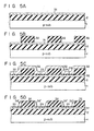
- Example 2 is applied to the manufacture of a volatile memory cell of MNOS structure.
- a field oxide film 2 was formed in a p-type silicon substrate 1 by the same procedure as in Example 1 described above.
- a p -type channel cut region 3 was formed in the portion of the substrate 1 which was in the vicinity of the field oxide film 2.
- oxidation was performed to 0 grow a thermal oxide film of 30 A thickness on the island-region of the substrate 1 isolated by the field oxide film 2.
- a silicon nitride film (Si 3 N 4 film) of 500 A thickness and a PSG film of 1.0 ⁇ m thickness were sequentially formed on the entire surface by the CVD method.
- a resist pattern (not shown) was formed on the PSG film by photolithography. Using the resist pattern as a mask, the underlying films were selectively etched to form a gate oxide film 8 and a two-layer protruding pattern 28 consisting of an Si 3 N 4 pattern 27 and a PSG pattern 10 thereon.
- n-type impurity e.g., arsenic was ion-implanted into the silicon substrate 1.
- the resist pattern was removed, and annealing was then performed to form shallow and low concentration n -type regions 13 1 and 14 1 .
- oxidation was performed to form a thermal oxide film 29 on the exposed surface of the substrate 1 (n -type regions 13 1 and 14 1 ), and a polysilicon film 15 of 5,000 A thickness was deposited on the entire surface by the CVD method.
- the polysilicon film 15 was etched by a distance corresponding to its thickness by RIE to leave a polysilicon film pattern 15' on the surface portion of the Si 3 N 4 pattern 27 and the PSG pattern 10 (protruding pattern 28). Subsequently, using the polysilicon film pattern 15' as a mask, the thermal oxide film 29 was selectively etched to form contact holes 16 for the source and drain and to leave a thermal oxide film pattern 29' below the polysilicon film pattern 15'.
- an n-type impurity e.g., phosphorus was ion-implanted or diffusion of POCl 3 was performed to form n +- type regions 13 2 and 14 2 in the n - -type regions 13 1 and 14 1 .
- the n +- type regions 13 2 and 14 2 had a greater junction depth than the n - -type regions 13 1 and 14 1 and had a high impurity concentration.
- the PSG pattern 10 was entirely etched by a diluted hydrofluoric acid etching solution or a freon-type dry etchant. Then, the polysilicon film pattern 15' upwardly protruded from the Si 3 N 4 pattern 27 and becomes fence-shaped.
- an electrode material film such as an Al film 17 was deposited on the entire surface. As shown in Fig. 4E, the Al film 17 was disconnected at the fence-shaped polysilicon film pattern 15', and the Al film did not remain around the fence-shaped polysilicon film pattern 15'.
- the fence-shaped polysilicon film pattern 15' was etched by isotropic dry etching such as plasma etching to lift off the Al film formed thereover.
- the Al film 17 was thus separated.
- the isolated separated Al pattern was selectively etched.
- Al electrodes 21, 22 and 30 were formed.
- the Al electrode 21 connected the contact hole 16 and the source consisting of the n -type region 13 1 and n +- type region 13 2 .
- the Al electrode 22 connected the contact hole 16 and the drain consisting of the n - -type region 14 1 and the n +- type region 14 2 .
- the Al gate electrode 30 was formed on the Si 3 N 4 pattern 27.
- an Si0 2 film 24 1.0 ⁇ m thick was formed on the entire surface by the CVD method.
- a through hole 25 was formed in the portion of the Si0 2 film 24 corresponding to a part of the Ai electrode 21.
- the Al film was patterned to form Al wiring strips 26, thus preparing a volatile memory cell of the MNOS structure.
- a high-performance and high-packaging density volatile memory cell can be formed in which the Al electrode 21 for the source, the Al electrode 22 for the drain, and the Al electrode 30 for the gate can be formed in self-alignment, and the Al electrode 30 for the gate can be formed in the order of submicrons.
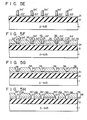
- Example 3 is applied to formation of wiring strips which connect the elements of a semiconductor device.
- a 0 first phosphorus-doped polysilicon film 31 of 2,000 A thickness was formed on the entire surface by the CVD method.
- SiO 2 film 1.0 ⁇ m thick on the entire surface by the CVD method it was patterned to form SiO 2 patterns (protruding patterns) 32.
- a second polysilicon 0 film 34 was deposited to a thickness of 4,000 A.
- the second polysilicon film 34 was etched by RIE to leave a polysilicon film patterns 34' on the surface portion of the SiO 2 patterns 32.
- the SiO 2 patterns 32 and the exposed portions of the thermal oxide film 33 were etched by RIE using a gas mixture of freon and hydrogen as an etchant.
- polysilicon film patterns 34' upwardly protruded from the first phosphorus-doped polysilicon film 31 and become fence-shaped, and thermal oxide film patterns 33' remained below these fence-shaped polysilicon film patterns 34'.
- an Al film 35 as a wiring film was vacuum-deposited by E-gan vacuum deposition or S-gan vacuum deposition. At this time, the Al film 35 was isolated at the fence-shaped polysilicon film patterns 34'. At the same time, the Al film did not remain at all or only remained to have a very small thickness around the fence-shaped polysilicon film patterns 34'. As shown in Fig. 5G, the fence-shaped polysilicon film patterns 34' were etched by dry etching using a freon-type etchant to lift off the Al film thereon and to form Al patterns 36.
- the At film can be etched within a short period and then the fence-shaped polysilicon film patterns 34' can be etched.
- the exposed thermal oxide film patterns 33' were etched by plasma etching using a gas mixture of freon and hydrogen as an etchant.
- the exposed first phosphorus-doped polysilicon film 31 was selectively etched to form polysilicon patterns 37, thus manufacturing two-layer wiring strips 38 consisting of the At patterns 36 and the polysilicon patterns 37.
- the two-layer wiring strips 38 can be easily formed which consists of the polysilicon patterns 37 and the Al patterns 36 which are separated by an extremely small distance which is determined by the width of the fence-shaped polysilicon film patterns 34'.
- the fence-shaped polysilicon film patterns were etched to lift off the Al film formed thereover so as to isolate or pattern the Al film.
- the present invention is not limited to this.
- the fence-shaped thin film patterns can be formed of an impurity-doped polysilicon. After depositing an undoped polysilicon film on the entire surface, thermal freatment is performed to selectively diffuse the impurity in the fence-shaped impurity-doped polysilicon film patterns to the surrounding undoped polysilicon film. Then, the impurity-doped portion of the undoped polysilicon film is etched to form wiring strips of polysilicon.
- the polysilicon thus obtained may be converted into a metal silicide to form wiring strips of low resistance.
- impurity is duffused from the fence-shaped impurity doped polysilicon film pattern to only that portion of the undoped polysilicon film which surrounds the protruding portion of the polysilion pattern.
- the wiring strips pitch can be made very small.
- the protruding pattern was a two-layer pattern consisting of a gate electrode of phosphorus-doped polysilicon and a PSG pattern, a two-layer pattern consisting of an Si 3 N 4 pattern and a PSG pattern, or an Si0 2 pattern.
- the protruding pattern may be a two-layer structure consisting of a semiconductor pattern and an insulation pattern.
- the semiconductor pattern of the protruding pattern can be used as an emitter region of an npn bipolar transistor, electrode matrial film may be isolated by fence-shaped thin film patterns formed on the surface of the semiconductor pattern.
- the base electrode and the emitter electrode may be isolated and may be formed with a high packaging density in self-alignment.
- the present invention allows mass production of semiconductor devices such as MOS LSIs which have improved packaging density and performance.
Abstract
Description
- The present invention relates to a method of manufacturing a semiconductor device and, more particularly, to a method of manufacturing a semiconductor device which has a step for forming electrodes and wiring strips, using self-aligned contact holes.
- Recent advances in techniques for manufacturing semiconductor devices and particularly semiconductor integrated circuits are significant. Improvements are particularly seen in photolithography, ion implantation, dry etching and so on. However, even if elements are micronized by these techniques, the packaging density is limited due to various restrictions in forming contact holes, positioning margin and in the like process.
- In view of this, a self-aligned contact (S.A.C.) technique is known as a method for forming a contact hole in self-alignment with a gate electrode in the manufacture of a MOS transistor. Such S.A.C. technique entitled as SELOCS (selective oxide coating of silicon gates) is published by HIDEO SUNAMI in Japanese Journal of Applied Physics, Vol. 18 (1979), pp. 255 to 260. According to this technique, a phosphorus-doped polycrystalline silicon (polysilicon) pattern having a high impurity concentration is formed on a gate oxide film which is formed on a p-type single crystal silicon substrate, and the polysilicon pattern thus formed is used as a gate electrode. Thermal oxidation is then performed to form a thick oxide film around the gate electrode and a thin oxide film on the exposed surface of the substrate. This is achieved because the oxidation rate of the phosphorus-doped polysilicon is greater than that of single crystal silicon. Thereafter, the oxide films are etched. The thin oxide film on the surface (source and drain) of the substrate is etched to expose the surface of the substrate, but the thick oxide film around the gate electrode partially remains. The exposed surface portion of the substrate is used as source and drain contact holes. The distances between the source and gate electrode and between the drain and gate electrode may therefore be minimized without requiring margins for positioning.
- However, this SELCOS method has various problems to be described below.
- The first problem is a low breakdown voltage of the thick oxide film around the gate electrode. In general, an oxide film which is obtained by etching has more enhanced defects and has greater characteristic variations than an epitaxially grown Si02 film. In particular, polysilicon doped with a high concentration of an impurity has a large crystal grain size and tends to have holes due to crystal interfaces or pinholes due to the photolithography process. For this reason, an oxide film obtained by thermally oxidizing a gate electrode made of such polysilicon of a high impurity concentration has poor characteristics. When such an oxide film is etched, a breakdown voltage (gate breakdown voltage, and breakdown voltage between the gate and source or between the source and drain) may be lowered.
- The second problem is an undesirable increase in the parasitic capacitance between the gate electrode and source or drain. This is attributed to the small thickness of the oxide film around the gate electrode, the small distances between the gate electrode and the source or drain electrodes, and the large opposing areas of these electrodes. Although this problem may be partially solved by circuit design or the like, this imposes further limitations on circuit design.
- The third problem is variations in the characteristics (fluctuations in the threshold voltage Vth). The difference in the oxidation rate of polysilicon and single crystal silicon by wet oxidation is reversely proportional to the oxidation temperature. However, an oxide film formed by wet oxidation at a low temperature has poor characteristics. Furthermore, the above-mentioned difference in oxidation rate increases with an increase in the concentration of the impurity in polysilicon. However, if the polysilicon of the gate electrode has a high impurity concentration, the impurity in the polysilicon is activated and diffused into the oxide film formed on the exposed surface of the single crystal silicon substrate. The impurity is further diffused from the oxide film into the substrate, causing further variations in the threshold voltage Vth.
- The fourth problem is as follows. When the oxide film around the gate electrode of polysilicon is made thicker for improved breakdown voltage, that is, when the thermal oxidation time is prolonged, the above-mentioned difference in the oxidation rate is reduced. Then, contact holes for source and drain may not be formed in self-alignment with the gate electrode.
- The fifth problem is that when a thick oxide film is formed around the gate electrode of polysilicon, the gate electrode is narrowed. Especially when the gate electrode has a step portion, disconnection may be caused at such a step portion. This is because it is very difficult to control the oxidation conditions and optimal setting of the impurity concentration in the polysilicon. When the gate electrode is micronized, the narrow gate electrode results in resistance increase and thus impairs high-speed and high-performance operation of the MOS transistor.
- The sixth problem is that micronization of a MOS transistor (semiconductor device) is limited since a positioning margin must be allowed between the source and drain electrodes. Since the source and drain electrodes overlap the oxide film on the gate electrode, a positioning margin (e.g., 1 to 2 µm) must be allowed between these electrodes if the electrodes are to be formed by photolithography. Therefore, if the MOS transistor is micronized, for example, with gate electrode width set to 1.0 µm, the source and drain electrodes cannot be formed with good precision unless the positioning margin is reduced to zero. However, it is practically impossible to reduce the margin to zero. Thus, although the SELCOS method is an excellent micronization technique which allows opening of contact holes in self-alignment with a gate electrode, it may not be effectively utilized. Furthermore, since the source and drain electrodes overlap the oxide film on the gate electrode, the parasitic capacitance increases between the overlapping portions of the gate electrode and the source and drain electrodes. This degrades performance of the MOS transistor.
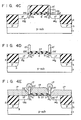
- Meanwhile, a method is proposed for forming a micronized gate electrode of a refractory metal silicide in the manufacture of a MOS transistor. Such a method is disclosed in Shinji Okazaki et al. "Edge-Defined Patterning of Hyperfine Refractory Metal Silicide MOS Structures" in IEEE TRANSACTION OF ELECTRON DEVICES, VOL. ED-28, NO-11, NOV. 1981, pp. 1364 to 1368. In this method, as shown in Figs. lA to 1D, a vertical edge is formed an oxide film which is formed on a silicon substrate through. A gate material (e.g, MOSi2) is deposited and covers the vertical edge. The gate material is selectively etched by anisotropic etching to leave the gate-material on the vertical edge and to form a gate electrode having hyperfine dimensions (< 1/4 pm). The vertical edge is then etched, and the exposed oxide film is selectively etched. Thus, in accordance with this method, the gate material left on the vertical edge is used to form a gate electrode having hyperfine dimensions.
- It is an object of the present invention to provide a method of manufacturing a semiconductor device, in which contact holes of impurity regions of a semiconductor body such as source and drain may be formed in self-alignment with a protruding pattern such as a gate electrode, and electrodes or wiring strips connected to the impurity regions through the contact holes can be formed in self-alignment with the protruding pattern (such as gate electrode), so that the semiconductor device may be micronized and may have high performance.
- In order to achieve the above object, a method of manufacturing a semiconductor device according to the present invention comprises the steps of:
- forming a thin film on a semiconductor body with a protruding pattern formed thereon;
- selectively leaving the thin film pattern surrounding at least a portion the protruding pattern; and
- etching at least the exposed portion of the protruding pattern, whereby said thin film pattern becomes fence-shaped.
- This invention can be more fully understood from the following detailed description when taken in conjunction with the accompanying drawings, in which:
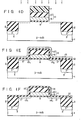
- Figs. lA to lL are views showing steps of a method of manufacturing an n-channel MOS LSI according to Example 1 of the present invention, wherein Figs. lA to 1I and 1L are sectional views and Figs. 1J and 1K are plan views;
- Fig. 2 is a sectional view showing another step of the method of manufacturing an n-channel MOS LSI according to Example 1 of the present invention;
- Fig. 3 is a sectional view showing another step of the method of manufacturing an n-channel MOS LSI according to Example 1 of the present invention;
- Figs. 4A to 4G are sectional views sequentially showing steps of a method for manufacturing a memory cell of MNOS structure according to Example 2 of the present invention; and
- Figs. 5A to 5H are sectional views sequentially showing steps of a method for forming wiring strips for a semiconductor device according to Example 3 of the present invention.
- A protruding pattern is formed on a semiconductor body directly or through an insulation film. The semiconductor body may be a semiconductor substrate of a first conductivity type, a semiconductor substrate of the first conductivity type with an epitaxial layer formed thereon or an epitaxial layer formed on an insulated substrate (e.g., a sapphire substrate). The protruding pattern may be a two-layer pattern consisting of a semiconductor pattern and an insulation pattern laminated thereover, a two-layer pattern consisting of a conductor pattern and an insulation pattern laminated thereover or a single- or two-layer insulation pattern. The conductor pattern may consist of an impurity-doped polysilicon, an impurity-doped amorphous silicon, a refractory metal, a metal silicide, aluminum, an aluminum alloy or the like. The conductor pattern may be obtained by forming a film of a starting material of undoped polysilicon or undoped amorphous silicon, and doping it with an impurity or siliciding it. The starting material of the insulation pattern may be an epitaxial silicon oxide film, a PSG film or a silicon nitride film. If the present invention is applied to the manufacture of MIS (Metal Insulator Semiconductor) transistors, an impurity of a second conductivity type is introduced (e.g., ion-implanted) into a semiconductor body (e.g., semiconductor substrate of the first conductivity type), using the protruding pattern as a mask, so as to form impurity regions of the second conductivity type.
- In the next step, a thin film is formed on the semiconductor body with the protruding pattern thereon directly or through an insulation film. The thin film must allow selective etching against the portion of the protruding pattern which is etched by an etching process to be described later. Furthermore, if the thin film is formed through the insulation film, the thin film must also allow selective etching against the insulation film. The thin film may be a polysilicon film, an amorphous silicon film, a silicon nitride film, a polyimide resin film or the like.
- The thin film is selectively etched by anisotropic etching (e.g., reactive ion etching, ion beam etching or the like), and the thin film pattern surrounding at least a portion the protruding pattern is left.
- At least an exposed portion (top part) of the protruding pattern is etched, whereby said thin film pattern becomes fence-shaped. If the insulation film is formed, the exposed portion of the insulation film is also etched. When impurity regions are formed in the semiconductor body in the manner as described above, the contact holes of the impurity regions are formed in self-alignment with the fence-shaped thin film pattern (or the protruding pattern).
- Then, an electrode material film or a wiring material film (e.g., a refractory material film, a metal silicide film, an aluminum film, or an aluminum alloy film) is deposited on the entire surface of the structure. The electrodes may be easily isolated by the fence-shaped thin film. Thereafter, the fence-shaped thin film is removed by etching so as to form electrodes or wiring strips between the now removed fence-shaped thin film pattern or around them if the fence-shaped thin film pattern is high and distances therebetween are small.
- In this manner, according to the present invention, electrodes or wiring strips are formed after forming fence-shaped thin film pattern. Therefore, electrodes or wiring strips may be formed between the fence-shaped thin film pattern as the fence-shaped thin film pattern serving as isolation films for the electrodes or wiring strips. In conventional techniques, the electrode pitch or the like is determined by photolithography, limiting micronization of the electrode pattern or the like. In contrast to this, according to the method of the present invention, the electrode pitch or the like is determined by the thickness of the thin film, that is, the width of the fence-shaped thin film pattern formed by anisotropic etching and an exposed portion of the protruding pattern is etched. Therefore, the electrodes or the wiring strips may be formed in the order of submicrons, resulting in higher packaging density of elements.
- If the thickness of the protruding pattern which determines the height of the remaining fence-shaped thin film pattern is increased, the height of the fence-shaped thin film pattern is not limited. As a result, by forming an electrode material film or the like after leaving a fence-shaped thin film pattern, the electrode film may be reliably isolated by the fence-shaped thin film pattern.
- The higher is the fence-shaped thin film pattern is, the easier it becomes to remove it by mechanical abrasion using by a jet scrubber or the like, in place of etching.
- According to the present invention, a low-resistance electrode or wiring strip may be formed which allows easy patterning and which consists of a refractory material such as Mo, W, Ta or Pt which is hard to etch.
- The present invention will now be described by ways of its examples with reference to the accompanying drawings.
- In Example 1, the present invention is applied to the manufacture of an n-channel MOS LSI.
- As shown in Fig. lA, after selectively ion-implanting a p-type impurity such as boron into a p-
type silicon substrate 1, selective oxidation was performed to form afield oxide film 2 and a p -typechannel cut region 3 in the vicinity of the bottom of thefield oxide film 2. Subsequently, as shown in Fig. lB, thermal oxidation was performed, thus forming a 0 thermal oxide film 4 400 A thick in an island-region of thesilicon substrate 1 isolated by thefield oxide film 2. Then, a phosphorus-dopedpolysilicon film 5 and a PSG film 6 each 500 A thick were formed. Thereafter, a resist pattern 7 was formed on the prospective gate electrode formation region of the PSG film 6. In this step, a BSG film, an SiO2 film or an Si3N4 film may be used in place of the PSG film. Then, as shown in Fig. 1C, the PSG film 6, thepolysilicon film 5 and the thermal oxide film 4 were selectively removed by reactive ion etching (RIE) using the resist pattern 7 as a mask, thus forming agate oxide film 8 and forming thereon a two-layer protruding pattern 11 consisting of agate electrode 9 and aPSG pattern 10. - Then, as shown in Fig. 1D, using the resist pattern 7 as a mask, an n-type impurity, e.g., arsenic was ion-implanted into the
silicon substrate 1. As shown in Fig. lE, after removing the resist pattern 7, a thermal oxide film (not shown) of about 300 A thickness was formed on the exposed surface of thesilicon substrate 1 by thermal oxidation. An SiO2 film 12 about 3,000 A thick was formed by the chemical vapor deposition (CVD) method on the entire surface. Annealing was then performed at 900°C to activate the ion-implanted arsenic to form shallow n -type regions 131 and 141 in thesilicon substrate 1. Thereafter, 0 apolysilicon film 15 4,000 A thick was deposited on the entire surface by the CVD method. Even if thegate electrode 9 is made of undoped polysilicon, the polysilicon can be converted into a low-resistance phosphorus-doped polysilicon by diffusing phosphorus from thePSG pattern 10. - Subsequently, the
polysilicon film 15 was etched by RIE for a distance corresponding to its thickness. Thus, as shown in Fig. 1F, a polysilicon film pattern 15' remained on the surface portion of the SiO2 film 12 corresponding to thegate electrode 9 and thePSG pattern 10. - As shown in Fig. lG, using the polysilicon film pattern 15' as a mask, the SiO2 film 12 and the thermal oxide film (not shown) were etched by RIE for a distance corresponding to their total thickness, thereby forming contact holes 16 corresponding to the n -
type regions 131 and 141 in self-alignment with thegate electrode 9. At the same time, an SiO2 film pattern 12' remained between the polysilicon film pattern 15' and thegate electrode 9. Subsequently, thePSG pattern 10 of the protruding pattern 11 was etched away. Then, the pattern 15' upwardly protrudes from thegate electrode 9 and becomes fence-shaped. Thereafter, using thegate electrode 9, the Si02 film pattern 12', the fence-shaped polysilicon film pattern 15' and thefield oxide film 2 as a mask, an n-type impurity e.g., phosphorus was ion-implanted or doped in a POCℓ3 atmosphere. Thus, n+-type regions 132 and 142 were formed on the exposed portions of the n--type regions 131 and 141 which were exposed through the contact holes 16. The n+-type regions 132 and 142 had a greater junction depth than the n--type regions 131 and 141 and had a high impurity concentration. Thegate electrode 9 was doped with phosphorus to have a low resistance. The n -type region 131 and the n+-type region 132 formed a source, and the n--type region 141 and the n -type region 142 formed a drain. - Then, as shown in Fig. lH, an electrode film such as an
Aℓ film 17 was deposited on the entire surface. Then, theAℓ film 17 was isolated by the fence-shaped polysilicon film pattern 15'. A very thin Aℓ film was formed or was not formed around the fence-shaped polysilicon film pattern 15'. As shown in Fig. lI, the fence-shaped polysilicon film pattern 15' was removed by isotropic dry etching, e.g., plasma etching. Thus, the Aℓ film on the fence-shaped polysilicon film pattern 15' was lifted off to isolate anAℓ pattern 19 which was formed on thegate electrode 9 andAℓ patterns 18 which were respectively connected through the contact holes 16 to the n -type region 131 and the n+-type region 132 (source) and to the n--type region 141 and the n -type region 142 (drain). If a very thin Aℓ film is deposited around the fence-shaped polysilicon film pattern 15', the Aℓ film can be etched for a short period of time to expose a part of the fence-shaped polysilicon film pattern 15'. Thereafter, the fence-shaped polysilicon film pattern 15' was removed by plasma etching or the like. The fence-shaped polysilicon film pattern 15' may alternatively be removed by mechanical abrasion using a jet scrubber or the like. - As shown in Fig. 1J, a resist
pattern 20 was formed by photolithography on theAℓ patterns pattern 20 as a mask, theAℓ patterns Aℓ electrodes gate electrode 9 was etched. The SiO2 film pattern 12' for isolation of theAℓ electrodes 21 to 23 remained on the side surfaces of thegate electrodes 9. However, the Si02 film pattern 12' on thefield oxide film 2 which does not serve to isolate theAℓ electrodes 21 to 23 may be removed by etching using the resistpattern 20 as a mask, or may be left on thefield oxide film 2. - As shown in Fig. 1L, after removing the
regist pattern 20, an SiO2 film 24 was deposited on the entire surface to a thickness of 1.0 µm by the CVD method. A throughhole 25 was formed on the portion of the Si02 film 24 on theAℓ electrode 21. An Aℓ film was vacuum-deposited on the entire surface and was patterned to form Aℓ wiring strips 26, thus completing a multilayered n-channel MOS LSI. - According to the present invention, the
polysilicon film 15 is deposited on the protruding pattern 11 through the Si02 film 12. Thepolysilicon film 15 is etched by a distance corresponding to its thickness by RIE to form the polysilicon film pattern 15'. Using the polysilicon film pattern 15' as a mask, the SiO2 film 12 and a thermal oxide film (not shown) are etched as well as thePSG pattern 10 as part of the protruding pattern 11. Thus, as shown in Fig. lG, the contact holes 16 for the source and drain are formed, and the polysilicon film pattern 15' becomes fence-shaped, and determines the distance between the contact holes 16 and thegate electrode 9. By etching the Si02 film 12 and the thermal oxide film (not shown) using the fence-shaped polysilicon film pattern 15' as a mask, a thin thermal oxide film (not shown) and the SiO2 film pattern 12' of excellent insulating property may be formed around thegate electrode 9 and below the fence-shaped polysilicon film pattern 15'. Therefore, satisfactory passivation effect and an improved gate breakdown voltage may be obtained to allow manufacture of a high-performance MOS LSI of high packaging density. - Furthermore, unlike the conventional methods, a gate electrode of an impurity-doped polysilicon need not be oxidized to form a thick thermal oxide film on the side surfaces of the gate electrode, reduction in the width of the gate electrode may be prevented, and a MOS LSI having an initially designed threshold voltage Vth may be obtained. The oxidation time during the manufacture of an MOS LSI can be reduced since such a thick oxide film need not be formed. Therefore, rediffusion of the impurity in the n-type regions as the source and drain is suppressed, so that the junction depths of these regions (especially the n--type regions 131 and 141) may be reduced to the minimum. In addition, rediffusion of the impurity in the p -type
channel cut region 3 may also be prevented. - As shown in Fig. 1L, according to the method of the present invention, since the
Aℓ electrode 23 of a low resistance can also be formed on thegate electrode 9 consisting of phosphorus-doped polysilicon, thegate electrode 9 may have a low resistance. As the gate electrode is micronized, the element characteristic is improved. However, the micronization in the gate electrode impaires the resistance increases and high-speed operation. Accordingly, in the method of the present invention, phosphorus-doped polysilicon is used to form thegate electrode 9. TheAℓ electrode 23 may be formed on thegate electrode 9 as needed. Therefore, theAℓ electrodes 21 to 23 for the source, drain and gate all have low resistances. This results in a high-speed operation of the MOS LSI. - Furthermore, according to the method of the present invention, the contact holes 16 for the source (the n -type region 131 and the n -type region 132) and the drain (n -
type region 141 and the n+-type region 142) may be formed in self-alignment with thegate electrode 9. TheAℓ electrodes gate electrode 9. With the conventional technique, the Aℓ electrodes for the source and drain are formed to overlap the gate electrode even if the contact holes for the source and drain can be formed in self-alignment with the gate electrode. This is inevitable because the Aℓ electrodes are formed and positioned by the photolithography. As a result, if the gate electrode is reduced in size to 1.5 pm, 1.0 µm or to the order of submicrons for improving the performance of the MOS LSI, At electrodes for the source and drain cannot be formed by the conventional photolithography. Thus, with the conventional photolithography, the contact holes formed in self-alignment with the gate electrode cannot be used for micronization of the element. In contrast, in the method of the present invention, the fence-shaped polysilicon film pattern 15' can isolate by self-alignment between thegate electrode 9 and theAℓ electrode 21 and between thegate electrode 9 and theAℓ electrode 22, as shown in Fig. lH. The width of the fence-shaped polysilicon film pattern 15' is determined by the thickness of thepolysilicon film 15 and can thus be controlled to a desired value. Moreover, processing in the order of submicrons may be performed between thegate electrode 9 and theAℓ electrode 21 and between thegate electrode 9 and theAℓ electrode 22, so that the width of thegate electrode 9 may be made in the order of submicrons. A micronized high-performance MOS LSI can thus be manufactured at a high yield. - As shown in Fig. 1D, in the method of the present invention, arsenic is ion-implanted in the
silicon substrate 1 to form shallow n -type regions 131 and 141 of low impurity concentration, using the protruding pattern 11 (resist pattern 7) and thefield oxide film 2 as a mask. As shown in Fig. 1G, using thegate electrode 9, the Si02 film pattern 12', the fence-shaped polysilicon film pattern 15' and thefield oxide film 2 as a mask, phosphorous or the like is ion-implanted into the n--type regions 131 and 141 exposed through the contact holes 16 to form n -type regions 132 and 142 having greater junction depth that of the n -type regions 131 and 141 and having a high impurity concentration. With such steps, a source can be formed in which the n--type region 131 is located near thegate electrode 9 and the n+-type region 132 is formed at a position far from the gate electrode 9 (corresponding to the contact hole 16). A drain having the n--type region 141 and the n+-type region 142 having a similar positional relationship may also be formed. When a voltage is applied to thegate electrode 9 and the drain to operate the MOS transistor, punch-through phenomenon due to micronization (shortening of the channel region) of thegate electrode 9 or variations in the threshold voltage Vth may be prevented. Since the portions of the source and drain which are exposed through the contact holes 16 comprise the n+-type regions 132 and 142, theAℓ electrodes - In Example 1 described above, the
PSG pattern 10 as part of the protruding pattern 11 is entirely etched so that the polysilicon film pattern 15' upwardly protrudes from thegate electrode 9 and becomes fence-shaped. TheAℓ electrode 23 is then formed on thegate electrode 9 by deposition and isolation of theAℓ film 17 so that thegate electrode 9 may have a low resistance. The method of the present invention is not limited to this. For example, as shown in Fig. 2, thePSG pattern 10 may be etched to leave a thin PSG pattern 10' on thegate electrode 9 as shown in Fig. 2 and a polysilicon film pattern 15' upwardly protrudes from the thin PSG pattern 10' and becomes fence-shaped. Then, theAt electrode 23 may be formed on the PSG pattern 10' by depositing an Aℓ film on the fence-shaped polysilicon film pattern 15' and separating it. TheAℓ electrode 23 may also be utilized as a wiring strip of another element. As shown in Fig. 3, a thick PSG pattern of 1.5 µm thickness is formed on thegate electrode 9 having dimensions of submicrons. Etching is performed, leaving the thick PSG pattern which is a fence-shaped polysilicon film pattern 15' protruding high. Thereafter, theAℓ film 17 is deposited, so that no At film may not be deposited on the PSG pattern 10' of thegate electrode 9 having dimensions in the order of submicrons by the blocking function of the fence-shaped polysilicon film pattern 15'. Referring to Fig. 3, if the portion of thegate electrode 9 consisting of MoSi2 which extends over thefield oxide film 2 has a great width, theAℓ film 17 is deposited on the PSG pattern 10' at this portion of thegate electrode 9. If the contact hole is formed in the portion of the PSG pattern 10' on the wide portion of thegate electrode 9, patterning of theAℓ film 17 will connect the Aℓ electrode to thegate electrode 9 through the contact hole. - Example 2 is applied to the manufacture of a volatile memory cell of MNOS structure.
- As shown in Fig. 4A, a
field oxide film 2 was formed in a p-type silicon substrate 1 by the same procedure as in Example 1 described above. A p -typechannel cut region 3 was formed in the portion of thesubstrate 1 which was in the vicinity of thefield oxide film 2. Subsequently, oxidation was performed to 0 grow a thermal oxide film of 30 A thickness on the island-region of thesubstrate 1 isolated by thefield oxide film 2. A silicon nitride film (Si3N4 film) of 500 A thickness and a PSG film of 1.0 µm thickness were sequentially formed on the entire surface by the CVD method. Subsequently, a resist pattern (not shown) was formed on the PSG film by photolithography. Using the resist pattern as a mask, the underlying films were selectively etched to form agate oxide film 8 and a two-layer protruding pattern 28 consisting of an Si3N4 pattern 27 and aPSG pattern 10 thereon. - Then, as shown in Fig. 4B, using the resist pattern (not shown) and the
field oxide film 2 as a mask, an n-type impurity, e.g., arsenic was ion-implanted into thesilicon substrate 1. Thereafter, the resist pattern was removed, and annealing was then performed to form shallow and low concentration n -type regions 131 and 141. Subsequently, oxidation was performed to form athermal oxide film 29 on the exposed surface of the substrate 1 (n -type regions 131 and 141), and apolysilicon film 15 of 5,000 A thickness was deposited on the entire surface by the CVD method. - As shown in Fig. 4C, the
polysilicon film 15 was etched by a distance corresponding to its thickness by RIE to leave a polysilicon film pattern 15' on the surface portion of the Si3N4 pattern 27 and the PSG pattern 10 (protruding pattern 28). Subsequently, using the polysilicon film pattern 15' as a mask, thethermal oxide film 29 was selectively etched to form contact holes 16 for the source and drain and to leave a thermal oxide film pattern 29' below the polysilicon film pattern 15'. Using thePSG pattern 10, the polysilicon film pattern 15', and thefield oxide film 2 as a mask, an n-type impurity, e.g., phosphorus was ion-implanted or diffusion of POCℓ3 was performed to form n+-type regions 132 and 142 in the n--type regions 131 and 141. The n+-type regions 132 and 142 had a greater junction depth than the n--type regions 131 and 141 and had a high impurity concentration. When theregions 132 and 142 were thus formed, a source consisting of the n -type region 131 and the n'-type region 132 and a drain consisting of the n--type region 141 and the n+-type region 142 were respectively formed. - As shown in Fig. 4D, the
PSG pattern 10 was entirely etched by a diluted hydrofluoric acid etching solution or a freon-type dry etchant. Then, the polysilicon film pattern 15' upwardly protruded from the Si3N4 pattern 27 and becomes fence-shaped. - Then, an electrode material film such as an
Aℓ film 17 was deposited on the entire surface. As shown in Fig. 4E, theAℓ film 17 was disconnected at the fence-shaped polysilicon film pattern 15', and the Aℓ film did not remain around the fence-shaped polysilicon film pattern 15'. - Then, as shown in Fig. 4F, the fence-shaped polysilicon film pattern 15' was etched by isotropic dry etching such as plasma etching to lift off the Aℓ film formed thereover. The
Aℓ film 17 was thus separated. As in Example 1, using a resist pattern (not shown) as a mask, the isolated separated Aℓ pattern was selectively etched. Thus,Aℓ electrodes Aℓ electrode 21 connected thecontact hole 16 and the source consisting of the n -type region 131 and n+-type region 132. TheAℓ electrode 22 connected thecontact hole 16 and the drain consisting of the n--type region 141 and the n+-type region 142. TheAℓ gate electrode 30 was formed on the Si3N4 pattern 27. - As shown in Fig. 4G, after removing the resist pattern, an Si02 film 24 1.0 µm thick was formed on the entire surface by the CVD method. A through
hole 25 was formed in the portion of the Si02 film 24 corresponding to a part of theAi electrode 21. After forming another Aℓ film by vacuum deposition, the Aℓ film was patterned to form Aℓ wiring strips 26, thus preparing a volatile memory cell of the MNOS structure. - According to this Example, a high-performance and high-packaging density volatile memory cell can be formed in which the
Aℓ electrode 21 for the source, theAℓ electrode 22 for the drain, and theAℓ electrode 30 for the gate can be formed in self-alignment, and theAℓ electrode 30 for the gate can be formed in the order of submicrons. - Example 3 is applied to formation of wiring strips which connect the elements of a semiconductor device.
- As shown in Fig. 5A, after selectively forming a
field oxide film 2 on a p-type silicon substrate 1, a 0 first phosphorus-dopedpolysilicon film 31 of 2,000 A thickness was formed on the entire surface by the CVD method. Subsequently, after forming an SiO2 film 1.0 µm thick on the entire surface by the CVD method, it was patterned to form SiO2 patterns (protruding patterns) 32. - Then, as shown in Fig. 5C, thermal oxidation was performed to grow a
thermal oxide film 33 on exposed the surface portion of the first phosphorus-dopedpolysilicon film 31. Thereafter, asecond polysilicon 0film 34 was deposited to a thickness of 4,000 A. Then, as shown in Fig. 5D, thesecond polysilicon film 34 was etched by RIE to leave a polysilicon film patterns 34' on the surface portion of the SiO2 patterns 32. - As shown in Fig. 5E, using the polysilicon film patterns 34' as a mask, the SiO2 patterns 32 and the exposed portions of the
thermal oxide film 33 were etched by RIE using a gas mixture of freon and hydrogen as an etchant. Thus, polysilicon film patterns 34' upwardly protruded from the first phosphorus-dopedpolysilicon film 31 and become fence-shaped, and thermal oxide film patterns 33' remained below these fence-shaped polysilicon film patterns 34'. - As shown in Fig. 5F, an
Aℓ film 35 as a wiring film was vacuum-deposited by E-gan vacuum deposition or S-gan vacuum deposition. At this time, theAℓ film 35 was isolated at the fence-shaped polysilicon film patterns 34'. At the same time, the Aℓ film did not remain at all or only remained to have a very small thickness around the fence-shaped polysilicon film patterns 34'. As shown in Fig. 5G, the fence-shaped polysilicon film patterns 34' were etched by dry etching using a freon-type etchant to lift off the Aℓ film thereon and to formAℓ patterns 36. If the Aℓ, film of small thickness remained below the fence-shaped polysilicon film patterns 34', the At film can be etched within a short period and then the fence-shaped polysilicon film patterns 34' can be etched. Subsequently, as shown in Fig. 5H, using theAt patterns 36 as a mask, the exposed thermal oxide film patterns 33' were etched by plasma etching using a gas mixture of freon and hydrogen as an etchant. Then, the exposed first phosphorus-dopedpolysilicon film 31 was selectively etched to formpolysilicon patterns 37, thus manufacturing two-layer wiring strips 38 consisting of theAt patterns 36 and thepolysilicon patterns 37. - In Example 3 described above, the two-layer wiring strips 38 can be easily formed which consists of the
polysilicon patterns 37 and theAℓ patterns 36 which are separated by an extremely small distance which is determined by the width of the fence-shaped polysilicon film patterns 34'. - In Examples 1 to 3 described above, the fence-shaped polysilicon film patterns were etched to lift off the Aℓ film formed thereover so as to isolate or pattern the Aℓ film. However, the present invention is not limited to this. For example, the fence-shaped thin film patterns can be formed of an impurity-doped polysilicon. After depositing an undoped polysilicon film on the entire surface, thermal freatment is performed to selectively diffuse the impurity in the fence-shaped impurity-doped polysilicon film patterns to the surrounding undoped polysilicon film. Then, the impurity-doped portion of the undoped polysilicon film is etched to form wiring strips of polysilicon. Alternatively, the polysilicon thus obtained may be converted into a metal silicide to form wiring strips of low resistance. In this case, impurity is duffused from the fence-shaped impurity doped polysilicon film pattern to only that portion of the undoped polysilicon film which surrounds the protruding portion of the polysilion pattern. As a result, the wiring strips pitch can be made very small.
- In Examples 1 to 3 described above, the protruding pattern was a two-layer pattern consisting of a gate electrode of phosphorus-doped polysilicon and a PSG pattern, a two-layer pattern consisting of an Si3N4 pattern and a PSG pattern, or an Si02 pattern. However, the protruding pattern may be a two-layer structure consisting of a semiconductor pattern and an insulation pattern. In this case, if the semiconductor pattern of the protruding pattern can be used as an emitter region of an npn bipolar transistor, electrode matrial film may be isolated by fence-shaped thin film patterns formed on the surface of the semiconductor pattern. Thus, the base electrode and the emitter electrode may be isolated and may be formed with a high packaging density in self-alignment.
- In summary, the present invention allows mass production of semiconductor devices such as MOS LSIs which have improved packaging density and performance.
Claims (29)
Applications Claiming Priority (2)
| Application Number | Priority Date | Filing Date | Title |
|---|---|---|---|
| JP41331/82 | 1982-03-16 | ||
| JP57041331A JPS58158972A (en) | 1982-03-16 | 1982-03-16 | Manufacture of semiconductor device |
Publications (3)
| Publication Number | Publication Date |
|---|---|
| EP0088922A2 true EP0088922A2 (en) | 1983-09-21 |
| EP0088922A3 EP0088922A3 (en) | 1985-07-03 |
| EP0088922B1 EP0088922B1 (en) | 1989-01-04 |
Family
ID=12605531
Family Applications (1)
| Application Number | Title | Priority Date | Filing Date |
|---|---|---|---|
| EP83101880A Expired EP0088922B1 (en) | 1982-03-16 | 1983-02-25 | A method of forming electrodes and wiring strips on a semiconductor device |
Country Status (4)
| Country | Link |
|---|---|
| US (1) | US4521448A (en) |
| EP (1) | EP0088922B1 (en) |
| JP (1) | JPS58158972A (en) |
| DE (1) | DE3378869D1 (en) |
Cited By (7)
| Publication number | Priority date | Publication date | Assignee | Title |
|---|---|---|---|---|
| EP0173953A2 (en) * | 1984-08-28 | 1986-03-12 | Kabushiki Kaisha Toshiba | Method for manufacturing a semiconductor device having a gate electrode |
| EP0315229A2 (en) * | 1987-10-05 | 1989-05-10 | Koninklijke Philips Electronics N.V. | Method of manufacturing a semiconductor device with insulated-gate structure |
| EP0322886A2 (en) * | 1987-12-28 | 1989-07-05 | Kabushiki Kaisha Toshiba | Method for manufacturing semiconductor device |
| GB2214349A (en) * | 1988-01-19 | 1989-08-31 | Standard Microsyst Smc | Process for fabricating mos devices |
| EP0351316A1 (en) * | 1988-07-13 | 1990-01-17 | Commissariat A L'energie Atomique | Process for manufacturing an integrated memory-cell |
| EP0399664A1 (en) * | 1989-05-23 | 1990-11-28 | Advanced Micro Devices, Inc. | Forming and removing polysilicon LDD spacers |
| US5212105A (en) * | 1989-05-24 | 1993-05-18 | Kabushiki Kaisha Toshiba | Semiconductor device manufacturing method and semiconductor device manufactured thereby |
Families Citing this family (32)
| Publication number | Priority date | Publication date | Assignee | Title |
|---|---|---|---|---|
| JPS6074682A (en) * | 1983-09-30 | 1985-04-26 | Toshiba Corp | Manufacture of semiconductor device |
| EP0159601A3 (en) * | 1984-04-10 | 1987-08-19 | Hartwig Wolfgang Prof.Dr. Thim | Logic circuit arrangement with appropriately constructed field-effect transistors |
| JPH0760864B2 (en) * | 1984-07-13 | 1995-06-28 | 株式会社日立製作所 | Semiconductor integrated circuit device |
| JPS61135149A (en) * | 1984-12-06 | 1986-06-23 | Toshiba Corp | Mos type integrated circuit |
| US5227319A (en) * | 1985-02-08 | 1993-07-13 | Kabushiki Kaisha Toshiba | Method of manufacturing a semiconductor device |
| JPS61287159A (en) * | 1985-06-13 | 1986-12-17 | Oki Electric Ind Co Ltd | Manufacture of bi-cmos semiconductor ic device |
| US4760433A (en) * | 1986-01-31 | 1988-07-26 | Harris Corporation | ESD protection transistors |
| US5256583A (en) * | 1986-03-21 | 1993-10-26 | Advanced Power Technology, Inc. | Mask surrogate semiconductor process with polysilicon gate protection |
| US4895810A (en) * | 1986-03-21 | 1990-01-23 | Advanced Power Technology, Inc. | Iopographic pattern delineated power mosfet with profile tailored recessed source |
| JPS62252891A (en) * | 1986-04-25 | 1987-11-04 | Sumitomo Heavy Ind Ltd | Counterflow floating plate type heat exchanger |
| US4794565A (en) * | 1986-09-15 | 1988-12-27 | The Regents Of The University Of California | Electrically programmable memory device employing source side injection |
| JP2705106B2 (en) * | 1988-05-25 | 1998-01-26 | セイコーエプソン株式会社 | Method for manufacturing semiconductor device |
| US4948745A (en) * | 1989-05-22 | 1990-08-14 | Motorola, Inc. | Process for elevated source/drain field effect structure |
| JP2995838B2 (en) * | 1990-01-11 | 1999-12-27 | セイコーエプソン株式会社 | Mis type semiconductor device and manufacture thereof |
| US5013398A (en) * | 1990-05-29 | 1991-05-07 | Micron Technology, Inc. | Anisotropic etch method for a sandwich structure |
| US5496750A (en) * | 1994-09-19 | 1996-03-05 | Texas Instruments Incorporated | Elevated source/drain junction metal oxide semiconductor field-effect transistor using blanket silicon deposition |
| US20020197838A1 (en) * | 1996-01-16 | 2002-12-26 | Sailesh Chittipeddi | Transistor fabrication method |
| US6225174B1 (en) | 1996-06-13 | 2001-05-01 | Micron Technology, Inc. | Method for forming a spacer using photosensitive material |
| CA2298491C (en) | 1997-07-25 | 2009-10-06 | Nichia Chemical Industries, Ltd. | Nitride semiconductor device |
| US5994239A (en) * | 1997-12-18 | 1999-11-30 | Advanced Micro Devices, Inc. | Manufacturing process to eliminate polystringers in high density nand-type flash memory devices |
| US6063668A (en) * | 1997-12-18 | 2000-05-16 | Advanced Micro Devices, Inc. | Poly I spacer manufacturing process to eliminate polystringers in high density nand-type flash memory devices |
| US6281078B1 (en) | 1997-12-18 | 2001-08-28 | Advanced Micro Devices, Inc. | Manufacturing process to eliminate ONO fence material in high density NAND-type flash memory devices |
| US6051487A (en) * | 1997-12-18 | 2000-04-18 | Advanced Micro Devices, Inc. | Semiconductor device fabrication using a sacrificial plug for defining a region for a gate electrode |
| US6448615B1 (en) | 1998-02-26 | 2002-09-10 | Micron Technology, Inc. | Methods, structures, and circuits for transistors with gate-to-body capacitive coupling |
| US6104066A (en) | 1998-03-30 | 2000-08-15 | Micron Technology, Inc. | Circuit and method for low voltage, voltage sense amplifier |
| JP3770014B2 (en) | 1999-02-09 | 2006-04-26 | 日亜化学工業株式会社 | Nitride semiconductor device |
| WO2000052796A1 (en) | 1999-03-04 | 2000-09-08 | Nichia Corporation | Nitride semiconductor laser element |
| US6197673B1 (en) * | 1999-06-08 | 2001-03-06 | United Semiconductor Corp. | Method of fabricating passivation of gate electrode |
| JP4468609B2 (en) * | 2001-05-21 | 2010-05-26 | 株式会社ルネサステクノロジ | Semiconductor device |
| TWI362769B (en) | 2008-05-09 | 2012-04-21 | Univ Nat Chiao Tung | Light emitting device and fabrication method therefor |
| US9236243B2 (en) | 2014-01-09 | 2016-01-12 | Stmicroelectronics Pte Ltd | Method for making semiconductor devices including reactant treatment of residual surface portion |
| US11063117B2 (en) * | 2017-04-20 | 2021-07-13 | Taiwan Semiconductor Manufacturing Co., Ltd. | Semiconductor device structure having carrier-trapping layers with different grain sizes |
Citations (1)
| Publication number | Priority date | Publication date | Assignee | Title |
|---|---|---|---|---|
| EP0043943A2 (en) * | 1980-07-08 | 1982-01-20 | International Business Machines Corporation | Method for forming field effect transistor integrated circuits having a pattern of narrow dimensioned dielectric regions and resulting structures |
Family Cites Families (1)
| Publication number | Priority date | Publication date | Assignee | Title |
|---|---|---|---|---|
| US4354896A (en) * | 1980-08-05 | 1982-10-19 | Texas Instruments Incorporated | Formation of submicron substrate element |
-
1982
- 1982-03-16 JP JP57041331A patent/JPS58158972A/en active Granted
-
1983
- 1983-02-25 DE DE8383101880T patent/DE3378869D1/en not_active Expired
- 1983-02-25 EP EP83101880A patent/EP0088922B1/en not_active Expired
- 1983-03-03 US US06/471,651 patent/US4521448A/en not_active Expired - Lifetime
Patent Citations (1)
| Publication number | Priority date | Publication date | Assignee | Title |
|---|---|---|---|---|
| EP0043943A2 (en) * | 1980-07-08 | 1982-01-20 | International Business Machines Corporation | Method for forming field effect transistor integrated circuits having a pattern of narrow dimensioned dielectric regions and resulting structures |
Non-Patent Citations (1)
| Title |
|---|
| IEEE TRANSACTIONS ON ELECTRON DEVICES, Vol. ED-28, No. 11, November 1981, pages 1364-1368 NEW YORK, (US) S. OKAZAKI, et al.:"Edge-defined patterning of hyperfin refractory metal silicide MOS structures". * |
Cited By (13)
| Publication number | Priority date | Publication date | Assignee | Title |
|---|---|---|---|---|
| EP0173953A3 (en) * | 1984-08-28 | 1988-01-13 | Kabushiki Kaisha Toshiba | Method for manufacturing a semiconductor device having a gate electrode |
| EP0173953A2 (en) * | 1984-08-28 | 1986-03-12 | Kabushiki Kaisha Toshiba | Method for manufacturing a semiconductor device having a gate electrode |
| EP0315229A3 (en) * | 1987-10-05 | 1991-04-17 | Koninklijke Philips Electronics N.V. | Method of manufacturing a semiconductor device with insulated-gate structure |
| EP0315229A2 (en) * | 1987-10-05 | 1989-05-10 | Koninklijke Philips Electronics N.V. | Method of manufacturing a semiconductor device with insulated-gate structure |
| EP0322886A2 (en) * | 1987-12-28 | 1989-07-05 | Kabushiki Kaisha Toshiba | Method for manufacturing semiconductor device |
| EP0322886A3 (en) * | 1987-12-28 | 1990-03-21 | Kabushiki Kaisha Toshiba | Method for manufacturing semiconductor device |
| GB2214349A (en) * | 1988-01-19 | 1989-08-31 | Standard Microsyst Smc | Process for fabricating mos devices |
| GB2214349B (en) * | 1988-01-19 | 1991-06-26 | Standard Microsyst Smc | Process for fabricating mos devices |
| EP0351316A1 (en) * | 1988-07-13 | 1990-01-17 | Commissariat A L'energie Atomique | Process for manufacturing an integrated memory-cell |
| FR2634318A1 (en) * | 1988-07-13 | 1990-01-19 | Commissariat Energie Atomique | METHOD FOR MANUFACTURING INTEGRATED MEMORY CELL |
| US5011787A (en) * | 1988-07-13 | 1991-04-30 | Commissariat A L'energie Atomique | Production of an integrated memory cell |
| EP0399664A1 (en) * | 1989-05-23 | 1990-11-28 | Advanced Micro Devices, Inc. | Forming and removing polysilicon LDD spacers |
| US5212105A (en) * | 1989-05-24 | 1993-05-18 | Kabushiki Kaisha Toshiba | Semiconductor device manufacturing method and semiconductor device manufactured thereby |
Also Published As
| Publication number | Publication date |
|---|---|
| JPH0479133B2 (en) | 1992-12-15 |
| US4521448A (en) | 1985-06-04 |
| JPS58158972A (en) | 1983-09-21 |
| DE3378869D1 (en) | 1989-02-09 |
| EP0088922A3 (en) | 1985-07-03 |
| EP0088922B1 (en) | 1989-01-04 |
Similar Documents
| Publication | Publication Date | Title |
|---|---|---|
| EP0088922B1 (en) | A method of forming electrodes and wiring strips on a semiconductor device | |
| EP0036082B1 (en) | A self-aligned process for providing an improved high performance bipolar transistor | |
| EP0173953B1 (en) | Method for manufacturing a semiconductor device having a gate electrode | |
| EP0366587B1 (en) | Semiconductor devices having closely spaced device regions formed using a self aligning reverse image fabrication process | |
| US4481706A (en) | Process for manufacturing integrated bi-polar transistors of very small dimensions | |
| US4803176A (en) | Integrated circuit structure with active device in merged slot and method of making same | |
| US6091117A (en) | Field effect transistor having elevated source and drain regions and methods of manufacturing the same | |
| US5118639A (en) | Process for the formation of elevated source and drain structures in a semiconductor device | |
| EP0061855A1 (en) | Method for manufacturing semiconductor device | |
| US4908324A (en) | Method of manufacturing bipolar transistor | |
| US4412378A (en) | Method for manufacturing semiconductor device utilizing selective masking, etching and oxidation | |
| EP0201867B1 (en) | Method of manufacturing a bipolar transistor | |
| JPS6219061B2 (en) | ||
| JPS6226590B2 (en) | ||
| EP0070402B1 (en) | Method of forming electrically conductive patterns on a semiconductor device, and a semiconductor device manufactured by the method | |
| US4822754A (en) | Fabrication of FETs with source and drain contacts aligned with the gate electrode | |
| EP0369336A2 (en) | Process for fabricating bipolar and CMOS transistors on a common substrate | |
| US5023192A (en) | Method of manufacturing a bipolar transistor | |
| EP0399231B1 (en) | Method of manufacturing a semiconductor device | |
| EP0281235B1 (en) | Bipolar transistor fabrication utilizing cmos techniques | |
| JPH0241170B2 (en) | ||
| EP0038079B1 (en) | Method for manufacturing a semiconductor integrated circuit device | |
| US5731240A (en) | Manufacturing method for semiconductor depositing device | |
| US5747374A (en) | Methods of fabricating bipolar transistors having separately formed intrinsic base and link-up regions | |
| US4926235A (en) | Semiconductor device |
Legal Events
| Date | Code | Title | Description |
|---|---|---|---|
| PUAI | Public reference made under article 153(3) epc to a published international application that has entered the european phase |
Free format text: ORIGINAL CODE: 0009012 |
|
| 17P | Request for examination filed |
Effective date: 19830322 |
|
| AK | Designated contracting states |
Designated state(s): DE FR GB IT |
|
| RAP1 | Party data changed (applicant data changed or rights of an application transferred) |
Owner name: KABUSHIKI KAISHA TOSHIBA |
|
| PUAL | Search report despatched |
Free format text: ORIGINAL CODE: 0009013 |
|
| AK | Designated contracting states |
Designated state(s): DE FR GB IT |
|
| 17Q | First examination report despatched |
Effective date: 19870515 |
|
| GRAA | (expected) grant |
Free format text: ORIGINAL CODE: 0009210 |
|
| AK | Designated contracting states |
Kind code of ref document: B1 Designated state(s): DE FR GB IT |
|
| ITF | It: translation for a ep patent filed |
Owner name: JACOBACCI & PERANI S.P.A. |
|
| REF | Corresponds to: |
Ref document number: 3378869 Country of ref document: DE Date of ref document: 19890209 |
|
| ET | Fr: translation filed | ||
| PLBE | No opposition filed within time limit |
Free format text: ORIGINAL CODE: 0009261 |
|
| STAA | Information on the status of an ep patent application or granted ep patent |
Free format text: STATUS: NO OPPOSITION FILED WITHIN TIME LIMIT |
|
| 26N | No opposition filed | ||
| ITTA | It: last paid annual fee | ||
| PGFP | Annual fee paid to national office [announced via postgrant information from national office to epo] |
Ref country code: FR Payment date: 19970211 Year of fee payment: 15 |
|
| PGFP | Annual fee paid to national office [announced via postgrant information from national office to epo] |
Ref country code: GB Payment date: 19970217 Year of fee payment: 15 |
|
| PGFP | Annual fee paid to national office [announced via postgrant information from national office to epo] |
Ref country code: DE Payment date: 19970228 Year of fee payment: 15 |
|
| PG25 | Lapsed in a contracting state [announced via postgrant information from national office to epo] |
Ref country code: GB Free format text: LAPSE BECAUSE OF NON-PAYMENT OF DUE FEES Effective date: 19980225 |
|
| PG25 | Lapsed in a contracting state [announced via postgrant information from national office to epo] |
Ref country code: FR Free format text: THE PATENT HAS BEEN ANNULLED BY A DECISION OF A NATIONAL AUTHORITY Effective date: 19980228 |
|
| GBPC | Gb: european patent ceased through non-payment of renewal fee |
Effective date: 19980225 |
|
| PG25 | Lapsed in a contracting state [announced via postgrant information from national office to epo] |
Ref country code: DE Free format text: LAPSE BECAUSE OF NON-PAYMENT OF DUE FEES Effective date: 19981103 |
|
| REG | Reference to a national code |
Ref country code: FR Ref legal event code: ST |